Microring and microdisk resonator integrated circuits on a silicon chip
Microring and microdisk resonator integrated circuits on a silicon chip
Microring and microdisk resonator integrated circuits on a silicon chip

You also want an ePaper? Increase the reach of your titles
YUMPU automatically turns print PDFs into web optimized ePapers that Google loves.
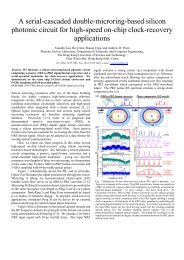
Fig. 7 (a) Calculated free-carrier induced refractive index change ∆n as a functi<strong>on</strong> of the metal-rim separati<strong>on</strong> up<strong>on</strong> 8-V reverse bias.Inset illustrates the metal-rim separati<strong>on</strong>. (b) Calculated ∆n as a functi<strong>on</strong> of p-doping c<strong>on</strong>centrati<strong>on</strong> in the <str<strong>on</strong>g>microdisk</str<strong>on</strong>g> rim. (c)Calculated ∆n temporal resp<strong>on</strong>se in the <str<strong>on</strong>g>microdisk</str<strong>on</strong>g> rim regi<strong>on</strong> (red) <str<strong>on</strong>g>and</str<strong>on</strong>g> in a (microring) waveguide (blue) from 0 V to -8 V <str<strong>on</strong>g>and</str<strong>on</strong>g> back to0 V. Inset: schematic cross-secti<strong>on</strong> of a (microring) waveguide with a laterally <str<strong>on</strong>g>integrated</str<strong>on</strong>g> Schottky diode of the same ohmic-to-Schottky separati<strong>on</strong> as in the <str<strong>on</strong>g>microdisk</str<strong>on</strong>g>. (d) Calculated ∆n rise <str<strong>on</strong>g>and</str<strong>on</strong>g> fall times as a functi<strong>on</strong> of the inner slab height (with fixed outerslab height at 0.03 µm). Inset illustrates the inner <str<strong>on</strong>g>and</str<strong>on</strong>g> outer slab heights. (e) Calculated ∆n rise <str<strong>on</strong>g>and</str<strong>on</strong>g> fall times as a functi<strong>on</strong> of theouter slab height (with fixed inner slab height at 0.21 µm).Fig. 7(c) shows the calculated ∆n temporal resp<strong>on</strong>se of a <str<strong>on</strong>g>microdisk</str<strong>on</strong>g> rim <str<strong>on</strong>g>and</str<strong>on</strong>g> a (microring) waveguide structure of thesame ohmic-to-Schottky separati<strong>on</strong> of 1.2 µm. Inset shows the waveguide cross secti<strong>on</strong>. The diode is revered-biasedfrom 0 V to -8 V <str<strong>on</strong>g>and</str<strong>on</strong>g> back to 0 V. The rise <str<strong>on</strong>g>and</str<strong>on</strong>g> fall times (~8 ps) of the <str<strong>on</strong>g>microdisk</str<strong>on</strong>g> are shorter than those of thewaveguide structure (23 ps – 14 ps). The electrical b<str<strong>on</strong>g>and</str<strong>on</strong>g>width of the Schottky diode is thus ~40 GHz. We attribute thefaster switching times of the <str<strong>on</strong>g>microdisk</str<strong>on</strong>g> than of the (microring) waveguide to the relatively low resistance provided by thelarger interface between the p + -doped central regi<strong>on</strong> <str<strong>on</strong>g>and</str<strong>on</strong>g> the <str<strong>on</strong>g>microdisk</str<strong>on</strong>g> rim regi<strong>on</strong>.In order to support the above argument, Fig. 7(d) shows the calculated ∆n rise <str<strong>on</strong>g>and</str<strong>on</strong>g> fall times at various inner slab heights(fixed outer slab height at 0.03 µm). Inset illustrates the inner <str<strong>on</strong>g>and</str<strong>on</strong>g> outer slab heights. An inner slab height of 0.21 µmcorresp<strong>on</strong>ds to the <str<strong>on</strong>g>microdisk</str<strong>on</strong>g> structure, whereas an inner slab height of 0.03 µm corresp<strong>on</strong>ds to the (microring)waveguide structure. The increase in the inner slab height increases the interface between the <str<strong>on</strong>g>microdisk</str<strong>on</strong>g> rim regi<strong>on</strong> <str<strong>on</strong>g>and</str<strong>on</strong>g>the p + -doped regi<strong>on</strong>, <str<strong>on</strong>g>and</str<strong>on</strong>g> thereby reduces the juncti<strong>on</strong> resistance. Fig. 7(c) shows the calculated ∆n rise <str<strong>on</strong>g>and</str<strong>on</strong>g> fall times atvarious outer slab heights. The effect of changing the outer slab height is less significant compared with varying theinner slab height because free-carriers (h + ) are swept in <str<strong>on</strong>g>and</str<strong>on</strong>g> out between the p + -doped central regi<strong>on</strong> <str<strong>on</strong>g>and</str<strong>on</strong>g> the p-doped rimregi<strong>on</strong> (but not via the Schottky c<strong>on</strong>tact).It should be emphasized that the b<str<strong>on</strong>g>and</str<strong>on</strong>g>width of a micro<str<strong>on</strong>g>res<strong>on</strong>ator</str<strong>on</strong>g>-based modulator is fundamentally limited by the phot<strong>on</strong>cavity lifetime τ as the res<strong>on</strong>ance mode needs time to build up <str<strong>on</strong>g>and</str<strong>on</strong>g> decay [36]. For a mode with Q ~ 10 4 , the decay time