

Geode GXLV Processor Series Low Power Integrated x86 Solutions
Geode GXLV Processor Series Low Power Integrated x86 Solutions
Geode GXLV Processor Series Low Power Integrated x86 Solutions

Create successful ePaper yourself
Turn your PDF publications into a flip-book with our unique Google optimized e-Paper software.
<strong>Geode</strong> <strong>GXLV</strong> <strong>Processor</strong> <strong>Series</strong>Table of Contents1.0 ArchitectureOverview.............................................101.1 INTEGERUNIT ..........................................................111.2 FLOATINGPOINTUNIT ...................................................111.3 WRITE-BACKCACHEUNIT ................................................111.4 MEMORYMANAGEMENTUNIT .............................................111.5 INTERNALBUSINTERFACEUNIT...........................................111.6 INTEGRATED FUNCTIONS . . . . ............................................121.6.1 Graphics Accelerator . . . ............................................121.6.2 DisplayController ..................................................121.6.3 XpressRAMMemorySubsystem ......................................121.6.4 PCIController.....................................................121.7 GEODE<strong>GXLV</strong>/CS5530SYSTEMDESIGNS ....................................131.7.1 ReferenceDesigns.................................................162.0 SignalDefinitions.................................................192.1 PINASSIGNMENTS ......................................................202.2 SIGNALDESCRIPTIONS ..................................................312.2.1 SystemInterfaceSignals ............................................312.2.2 PCIInterfaceSignals ...............................................332.2.3 MemoryControllerInterfaceSignals ...................................362.2.4 VideoInterfaceSignals .............................................372.2.5 <strong>Power</strong>,Ground,andNoConnectSignals................................392.2.6 InternalTestandMeasurementSignals.................................393.0 <strong>Processor</strong>Programming ...........................................413.1 COREPROCESSORINITIALIZATION ........................................413.2 INSTRUCTIONSETOVERVIEW.............................................423.2.1 LockPrefix .......................................................423.3 REGISTERSETS.........................................................433.3.1 ApplicationRegisterSet.............................................433.3.1.1 GeneralPurposeRegisters ..........................................433.3.1.2 SegmentRegisters ................................................453.3.1.3 InstructionPointerRegister ..........................................453.3.1.4 EFLAGSRegister .................................................463.3.2 SystemRegisterSet ...............................................473.3.2.1 ControlRegisters..................................................483.3.2.2 ConfigurationRegisters .............................................503.3.2.3 DebugRegisters ..................................................553.3.2.4 TLBTestRegisters ................................................573.3.2.5 CacheTestRegisters ..............................................593.3.3 ModelSpecificRegisterSet ..........................................623.3.4 TimeStampCounter ...............................................623.4 ADDRESSSPACES.......................................................633.4.1 I/OAddressSpace .................................................633.4.2 MemoryAddressSpace.............................................64www.national.com 4 Revision 1.3
Table of Contents (Continued)3.5 OFFSET,SEGMENT,ANDPAGINGMECHANISMS .............................643.5.1 Offset Mechanism . . . . . ............................................643.5.2 SegmentMechanisms ..............................................663.5.2.1 RealModeSegmentMechanism .....................................663.5.2.2 Virtual8086ModeSegmentMechanism................................663.5.2.3 SegmentMechanisminProtectedMode................................673.5.2.4 SegmentSelectors ................................................673.5.3 Descriptors .......................................................703.5.3.1 GlobalandLocalDescriptorTableRegisters.............................703.5.3.2 SegmentDescriptors ...............................................703.5.3.3 Task, Gate, Interrupt, and Application and System Descriptors . . . . . . . . . . . . . . 713.5.4 PagingMechanism.................................................773.6 INTERRUPTSANDEXCEPTIONS ...........................................793.6.1 Interrupts ........................................................793.6.2 Exceptions .......................................................793.6.3 InterruptVectors ...................................................803.6.3.1 InterruptVectorAssignments.........................................803.6.3.2 InterruptDescriptorTable ...........................................803.6.4 InterruptandExceptionPriorities ......................................813.6.5 ExceptionsinRealMode ............................................823.6.6 ErrorCodes ......................................................823.7 SYSTEMMANAGEMENTMODE ............................................833.7.1 SMMOperation ...................................................843.7.2 SMI#Pin.........................................................853.7.3 SMMConfigurationRegisters ........................................853.7.4 SMMMemorySpaceHeader.........................................853.7.5 SMMInstructions ..................................................873.7.6 SMMMemorySpace ...............................................883.7.7 SMIGenerationforVirtualVGA .......................................883.7.8 SMMServiceRoutineExecution ......................................883.7.8.1 SMINesting ......................................................883.7.8.2 CPUStatesRelatedtoSMMandSuspendMode.........................903.8 HALTANDSHUTDOWN ...................................................913.9 PROTECTION ...........................................................913.9.1 PrivilegeLevels ...................................................913.9.2 I/OPrivilegeLevels ................................................913.9.3 PrivilegeLevelTransfers ............................................923.9.3.1 Gates ...........................................................933.9.4 InitializationandTransitiontoProtectedMode............................933.10 VIRTUAL8086MODE .....................................................933.10.1 MemoryAddressing ................................................933.10.2 Protection ........................................................933.10.3 Interrupt Handling . . . . . . ............................................933.10.4 EnteringandLeavingVirtual8086Mode................................933.11 FLOATINGPOINTUNITOPERATIONS .......................................943.11.1 FPURegisterSet ..................................................943.11.2 FPUTagWordRegister .............................................943.11.3 FPUStatusRegister ...............................................943.11.4 FPUModeControlRegister ..........................................94<strong>Geode</strong> <strong>GXLV</strong> <strong>Processor</strong> <strong>Series</strong>Revision 1.3 5 www.national.com
<strong>Geode</strong> <strong>GXLV</strong> <strong>Processor</strong> <strong>Series</strong>Table of Contents (Continued)4.0 <strong>Integrated</strong> Functions . . . . . . . . . . . . . . . . . . . . . . . . . . . . . . . . . . . . . . . . . . . . . . 964.1 INTEGRATED FUNCTIONS PROGRAMMING INTERFACE . . . . . . . . ...............974.1.1 Graphics Control Register . . . . . . . . . . . . . . . ............................974.1.2 ControlRegisters ..................................................994.1.3 Graphics Memory . . . . . . ............................................994.1.4 ScratchpadRAM .................................................1004.1.4.1 InitializationofScratchpadRAM .....................................1004.1.4.2 ScratchpadRAMUtilization.........................................1004.1.4.3 BLTBuffer ......................................................1004.1.5 DisplayDriverInstructions ..........................................1024.1.6 CPU_READ/CPU_WRITEInstructions ................................1024.2 INTERNALBUSINTERFACEUNIT..........................................1034.2.1 FPUErrorSupport ................................................1034.2.2 A20MSupport ...................................................1034.2.3 SMIGeneration ..................................................1034.2.4 640KBto1MBRegion ............................................1034.2.5 InternalBusInterfaceUnitRegisters ..................................1044.3 MEMORYCONTROLLER .................................................1074.3.1 MemoryArrayConfiguration ........................................1084.3.2 MemoryOrganizations .............................................1094.3.3 SDRAMCommands...............................................1104.3.3.1 SDRAMInitializationSequence......................................1114.3.4 MemoryControllerRegisterDescription ...............................1124.3.5 AddressTranslation ...............................................1174.3.5.1 HighOrderInterleaving ............................................1174.3.5.2 Auto<strong>Low</strong>OrderInterleaving ........................................1174.3.5.3 PhysicalAddresstoDRAMAddressConversion ........................1174.3.6 MemoryCycles ..................................................1204.3.7 SDRAMInterfaceClocking..........................................1234.4 GRAPHICSPIPELINE ....................................................1254.4.1 BitBLT/VectorEngine ..............................................1254.4.2 Master/SlaveRegisters ............................................1264.4.3 PatternGeneration ................................................1264.4.3.1 MonochromePatterns .............................................1274.4.3.2 DitherPatterns...................................................1274.4.3.3 ColorPatterns ...................................................1284.4.4 SourceExpansion ................................................1284.4.5 RasterOperations ................................................1284.4.6 Graphics Pipeline Register Descriptions . . . . ...........................129www.national.com 6 Revision 1.3
Table of Contents (Continued)4.5 DISPLAYCONTROLLER..................................................1344.5.1 DisplayFIFO ....................................................1354.5.2 CompressionTechnology ...........................................1354.5.3 HardwareCursor .................................................1364.5.4 DisplayTimingGenerator...........................................1364.5.5 DitherandFrameRateModulation ...................................1364.5.6 DisplayModes ...................................................1364.5.7 Graphics Memory Map . . ...........................................1404.5.7.1 DCMemoryOrganizationRegisters ..................................1404.5.7.2 FrameBufferandCompressionBufferOrganization......................1404.5.7.3 VGADisplaySupport..............................................1414.5.8 DisplayControllerRegisters.........................................1414.5.8.1 ConfigurationandStatusRegisters...................................1444.5.9 MemoryOrganizationRegisters......................................1484.5.10 TimingRegisters .................................................1504.5.11 CursorPositionandMiscellaneousRegisters ...........................1524.5.12 PaletteAccessRegisters ...........................................1534.5.13 FIFODiagnosticRegisters ..........................................1544.5.14 CS5530DisplayControllerInterface ..................................1554.5.14.1 CS5530VideoPortDataTransfer ....................................1564.6 VIRTUALVGASUBSYSTEM...............................................1574.6.1 TraditionalVGAHardware ..........................................1574.6.1.1 VGAMemoryOrganization .........................................1584.6.1.2 VGAFrontEnd...................................................1584.6.1.3 AddressMapping.................................................1584.6.1.4 VideoRefresh ...................................................1594.6.1.5 VGAVideoBIOS .................................................1594.6.2 VirtualVGA .....................................................1594.6.2.1 DatapathElements ...............................................1604.6.2.2 <strong>GXLV</strong>VGAHardware .............................................1604.6.2.3 SMIGeneration ..................................................1614.6.2.4 VGARangeDetection .............................................1614.6.2.5 VGASequencer..................................................1614.6.2.6 VGAWrite/ReadPath .............................................1614.6.2.7 VGAAddressGenerator ...........................................1614.6.2.8 VGAMemory ....................................................1614.6.3 VGAConfigurationRegisters ........................................1624.6.4 VirtualVGARegisterDescriptions ....................................1644.7 PCICONTROLLER ......................................................1664.7.1 X-BusPCISlave..................................................1664.7.2 X-BusPCIMaster ................................................1664.7.3 PCIArbiter ......................................................1664.7.4 GeneratingConfigurationCycles .....................................1664.7.5 GeneratingSpecialCycles..........................................1664.7.6 PCIConfigurationSpaceControlRegisters .............................1674.7.7 PCIConfigurationSpaceRegisters ...................................1684.7.8 PCICycles ......................................................1734.7.8.1 PCIReadTransaction .............................................1734.7.8.2 PCIWriteTransaction .............................................1744.7.8.3 PCIArbitration ...................................................1754.7.8.4 PCIHaltCommand ...............................................175<strong>Geode</strong> <strong>GXLV</strong> <strong>Processor</strong> <strong>Series</strong>Revision 1.3 7 www.national.com
<strong>Geode</strong> <strong>GXLV</strong> <strong>Processor</strong> <strong>Series</strong>Table of Contents (Continued)5.0 <strong>Power</strong>Management ..............................................1765.1 POWERMANAGEMENTFEATURES ........................................1765.1.1 SystemManagementMode .........................................1765.1.2 Suspend-on-Halt .................................................1765.1.3 CPUSuspend ...................................................1765.1.3.1 SuspendModulationforThermalManagement .........................1775.1.3.2 SuspendModulationfor<strong>Power</strong>Management ...........................1775.1.4 3VoltSuspend ...................................................1775.1.5 <strong>GXLV</strong><strong>Processor</strong>SerialBus .........................................1775.1.6 Advanced<strong>Power</strong>Management(APM)Support ..........................1775.2 SUSPENDMODESANDBUSCYCLES ......................................1785.2.1 TimingDiagramforSuspend-on-Halt..................................1785.2.2 InitiatingSuspendwithSUSP# ......................................1795.2.3 Stopping the Input Clock ...........................................1805.2.4 SerialPacketTransmission .........................................1805.3 POWERMANAGEMENTREGISTERS .......................................1816.0 ElectricalSpecifications ..........................................1846.1 PARTNUMBERS/PERFORMANCECHARACTERISTICS ........................1846.2 ELECTRICALCONNECTIONS .............................................1856.2.1 <strong>Power</strong>/GroundConnectionsandDecoupling ............................1856.2.1.1 <strong>Power</strong>Planes....................................................1856.2.2 NC-DesignatedPins...............................................1876.2.3 Pull-UpandPull-DownResistors .....................................1876.2.4 UnusedInputPins ................................................1876.3 ABSOLUTEMAXIMUMRATINGS ...........................................1886.4 OPERATINGCONDITIONS................................................1896.5 DCCHARACTERISTICS ..................................................1906.5.1 Input/OutputDCCharacteristics .....................................1906.5.2 DCCurrent ......................................................1906.5.2.1 DefinitionofCPU<strong>Power</strong>States......................................1906.5.2.2 Definition and Measurement Techniques of CPU Current Parameters . . . . . . . . 1906.5.2.3 Definition of System Conditions for Measuring "On" Parameters . . . . . . . . . . . . 1916.5.2.4 DCCurrentMeasurements .........................................1926.6 I/O CURRENT DE-RATING CURVE . . . . . . . . . . . . . . ...........................1956.6.1 DisplayResolution ................................................1956.6.2 MemorySpeed...................................................1956.6.3 I/OCurrentDe-ratingCurve .........................................1956.7 ACCHARACTERISTICS ..................................................196www.national.com 8 Revision 1.3
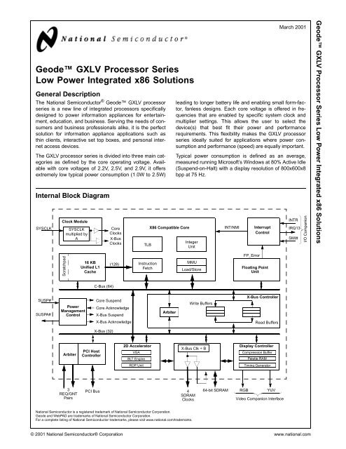
<strong>Geode</strong> <strong>GXLV</strong> <strong>Processor</strong> <strong>Series</strong>1.0 Architecture OverviewThe <strong>Geode</strong> <strong>GXLV</strong> processor series represents the sixthgeneration of <strong>x86</strong>-compatible 32-bit processors with sixthgenerationfeatures. The decoupled load/store unit allowsreordering of load/store traffic to achieve higher performance.Other features include single-cycle execution, single-cycleinstruction decode, 16 KB write-back cache, andclock rates up to 266 MHz. These features are made possibleby the use of advanced-process technologies andpipelining.The <strong>GXLV</strong> processor has low power consumption at allclock frequencies. Where additional power savings arerequired, designers can make use of Suspend Mode, StopClock capability, and System Management Mode (SMM).The <strong>GXLV</strong> processor is divided into major functionalblocks (as shown in Figure 1-1):• Integer Unit• Floating Point Unit (FPU)• Write-Back Cache Unit• Memory Management Unit (MMU)• Internal Bus Interface Unit• <strong>Integrated</strong> FunctionsInstructions are executed in the integer unit and in thefloating point unit. The cache unit stores the most recentlyused data and instructions and provides fast access tothis information for the integer and floating point units.Write-BackCache UnitMMUIntegerUnitFPUC-BusInternal Bus Interface UnitX-Bus<strong>Integrated</strong>FunctionsGraphics Memory Display PCIPipeline Controller Controller ControllerSDRAM Port CS5530 PCI Bus(CRT/LCD TFT)Figure 1-1. Internal Block Diagramwww.national.com 10 Revision 1.3
<strong>Geode</strong> <strong>GXLV</strong> <strong>Processor</strong> <strong>Series</strong>Architecture Overview (Continued)1.6 INTEGRATED FUNCTIONSThe <strong>GXLV</strong> processor integrates the following functions traditionallyimplemented using external devices:• High-performance 2D graphics accelerator• Separate CRT and TFT control from the displaycontroller• SDRAM memory controller• PCI bridgeThe processor has also been enhanced to support VSAtechnology implementation.The <strong>GXLV</strong> processor implements a Unified Memory Architecture(UMA). By using DCT (Display Compression Technology)architecture, the performance degradationinherent in traditional UMA systems is eliminated.1.6.1 Graphics AcceleratorThe graphics accelerator is a full-featured GUI accelerator.The graphics pipeline implements a bitBLT engine forframe buffer bitBLTs and rectangular fills. Additionalinstructions in the integer unit may be processed, as thebitBLT engine assists the CPU in the bitBLT operationsthat take place between system memory and the framebuffer. This combination of hardware and software is usedby the display driver to provide very fast bidirectionaltransfers between system memory and the frame buffer.The bitBLT engine also draws randomly oriented vectors,and scanlines for polygon fill. All of the pipeline operationsdescribed in the following list can be applied to any bitBLToperation.• Pattern Memory: Render with 8x8 dither, 8x8 monochrome,or 8x1 color pattern.• Color Expansion: Expand monochrome bitmaps tofull depth 8- or 16-bit colors.• Transparency: Suppresses drawing of backgroundpixels for transparent text.• Raster Operations: Boolean operation combinessource, destination, and pattern bitmaps.1.6.2 Display ControllerThe display port is a direct interface to the <strong>Geode</strong> I/Ocompanion (i.e., CS5530, part number 25420-03) whichdrives a TFT flat panel display, LCD panel, or a CRT display.The display controller (video generator) retrieves imagedata from the frame buffer, performs a color-look-up ifrequired, inserts the cursor overlay into the pixel stream,generates display timing, and formats the pixel data foroutput to a variety of display devices. The display controllercontains DCT architecture that allows the <strong>GXLV</strong> processorto refresh the display from a compressed copy ofthe frame buffer. DCT architecture typically decreases thescreen refresh bandwidth requirement by a factor of 15 to20, minimizing bandwidth contention.1.6.3 XpressRAM Memory SubsystemThe memory controller drives a 64-bit SDRAM portdirectly. The SDRAM memory array contains both themain system memory and the graphics frame buffer. Up tofour module banks of SDRAM are supported. Each modulebank can have two or four component banks dependingon the memory size and organization. The maximumconfiguration is four module banks with four componentbanks, each providing a total of 16 open banks. The maximummemory size is 256 MB.The memory controller handles multiple requests formemory data from the <strong>GXLV</strong> processor, the graphicsaccelerator and the display controller. The memory controllercontains extensive buffering logic that helps minimizecontention for memory bandwidth between graphicsand CPU requests. The memory controller cooperateswith the internal bus controller to determine the cacheabilityof all memory references.1.6.4 PCI ControllerThe <strong>GXLV</strong> processor incorporates a full-function PCIinterface module that includes the PCI arbiter. Allaccesses to external I/O devices are sent over the PCIbus, although most memory accesses are serviced by theSDRAM controller. The internal bus interface unit containsaddress mapping logic that determines if memoryaccesses are targeted for the SDRAM or for the PCI bus.www.national.com 12 Revision 1.3
Architecture Overview (Continued)1.7 GEODE <strong>GXLV</strong>/CS5530 SYSTEM DESIGNSA <strong>GXLV</strong> processor and <strong>Geode</strong> CS5530 I/O companionbased design provides high performance using 32-bit <strong>x86</strong>processing. The two chips integrate video, audio andmemory interface functions normally performed by externalhardware. The CS5530 enables the full features of the<strong>GXLV</strong> processor with MMX support. These featuresinclude full VGA and VESA video, 16-bit stereo sound,IDE interface, ISA interface, SMM power management,and IBM’s AT compatibility logic. In addition, the CS5530provides an Ultra DMA/33 interface, MPEG1 assist, andAC97 Version 2.0 compliant audio.Figure 1-2 shows a basic block system diagram whichalso includes the <strong>Geode</strong> CS9210 graphics companion fordesigns that need to interface to a Dual Scan SuperTwisted Pneumatic (DSTN) panel (instead of a TFTpanel).Figure 1-3 shows an example of a CS9210 interface in atypical <strong>GXLV</strong>/CS5530 based system design. The CS9210converts the digital RGB output of the CS5530 to the digitaloutput suitable for driving a color DSTN flat panel LCD.It can drive all standard color DSTN flat panels up to a1024x768 resolution.Figures 1-4 and 1-5 show the signal connections betweenthe <strong>GXLV</strong> processor and the CS5530. For connections tothe CS9210, refer to the CS9210 data book.<strong>Geode</strong> <strong>GXLV</strong> <strong>Processor</strong> <strong>Series</strong>SDRAMUSB(2 Ports)MD[63:0]ClocksSDRAMPortSerialPacket<strong>Geode</strong><strong>GXLV</strong><strong>Processor</strong>PCI InterfaceYUV Port(Video)RGB Port(Graphics)CRTSpeakersCDROMAudioAC97Codec<strong>Geode</strong>CS5530I/O CompanionGraphics DataVideo DataAnalog RGBPCI BusDigital RGB (to TFT or DSTN Panel)IDE ControlTFTPanelMicrophoneGPIO14.31818MHz CrystalSuperI/OBIOSIDEDevices<strong>Geode</strong>CS9210GraphicsCompanionDC-DC & BatteryISA BusDSTN PanelFigure 1-2. <strong>Geode</strong> <strong>GXLV</strong>/CS5530 System Block DiagramRevision 1.3 13 www.national.com
Architecture Overview (Continued)<strong>Geode</strong> <strong>GXLV</strong><strong>Processor</strong>RPIXEL17PIXEL16PIXEL15PIXEL14PIXEL13PIXEL12PIXEL23PIXEL22PIXEL21PIXEL20PIXEL19PIXEL18PIXEL17PIXEL16<strong>Geode</strong> CS5530I/O Companion<strong>Geode</strong> <strong>GXLV</strong> <strong>Processor</strong> <strong>Series</strong>PIXEL11PIXEL15PIXEL10PIXEL14GPIXEL9PIXEL8PIXEL13PIXEL12PIXEL7PIXEL11PIXEL6PIXEL10PIXEL9PIXEL8PIXEL5PIXEL7PIXEL4PIXEL6BPIXEL3PIXEL2PIXEL5PIXEL4PIXEL1PIXEL3PIXEL0PIXEL2PIXEL1PIXEL0Figure 1-5. PIXEL Signal ConnectionsRevision 1.3 15 www.national.com
<strong>Geode</strong> <strong>GXLV</strong> <strong>Processor</strong> <strong>Series</strong>Architecture Overview (Continued)NSCLM4549Codec<strong>Geode</strong><strong>GXLV</strong><strong>Processor</strong>1.7.1 Reference DesignsAs described previously, the <strong>GXLV</strong> series of integratedprocessors is designed specifically to work with National’s<strong>Geode</strong> I/O and graphics companion devices. To helpdefine and drive the emerging information appliance market,several reference systems have been developed byNational Semiconductor. These <strong>GXLV</strong> processor basedreference systems provide optimized and targeted solutionsfor three main segments of the information appliancemarket: Personal Internet Access, Thin Client, and SettopBox. Contact your local National Semiconductor salesor field support representative for further information onreference designs for the information appliance market.PCI BusControlDataSDRAMPCMCIAFlashCardOptionalEmbedded OSApplicationsBootloaderRun-Time DiagnosticsStorageUltra DMA/33USB Port<strong>Geode</strong>CS5530I/OCompanionISA BusRF InterfaceLinearFlash(8 MB)Embedded OSApplicationsBootloaderRun-Time DiagnosticsStorageButtonsPwr MgmtDC SenseMicrocontrollerBacklightDSTN<strong>Geode</strong>CS9210/11GraphicsCompanionLi Batteries/ChargerTouchControl512 KB DRAMFigure 1-6. Example WebPAD System Diagramwww.national.com 16 Revision 1.3
Architecture Overview (Continued)SDRAM SO-DIMMTFTUSB (2x)CRT<strong>Geode</strong> <strong>GXLV</strong> <strong>Processor</strong> <strong>Series</strong><strong>Geode</strong><strong>GXLV</strong><strong>Processor</strong>VideoPCI Bus<strong>Geode</strong>CS5530I/OCompanionNSCLM4546CodecMIC InAudio OutNSCDP83815EthernetControllerTerminationISA BusTermination64 MB FlashNSCPC97317IBW/VULSuperI/OResetPWR CTLCPU Core<strong>Power</strong><strong>Power</strong>ClockGeneratorMK1491-06Figure 1-7. Example Thin Client System DiagramRevision 1.3 17 www.national.com
<strong>Geode</strong> <strong>GXLV</strong> <strong>Processor</strong> <strong>Series</strong>Architecture Overview (Continued)AC3AnlgMIC MIC1 2IN INCPU Temp.SensorNSCLM75<strong>Geode</strong><strong>GXLV</strong><strong>Processor</strong>PCI BusSDRAM DIMMSDRAM DIMMDMAArbiterRiser SlotPCI SlotOptionalLAN PCICardLAN /WANHeadphoneOutputAudio LineOutputTunerFM InLM4548CodecCD In<strong>Geode</strong>CS5530I/OCompanionOptionalV.90ModemSDRAMC-CUBE“ZIVA”IGS 50x5GraphicsSGRAMSGRAMVideo PortVGAS-VideoPAL orNTSCISA SlotRiser SlotSAA7112CompositeVideo InNotebook DVDDrive2.5” UDMA-33Hard DriveNotebookFloppyDriveFlashBIOSISA BusROM SlotWinCE ROMModuleNSCPC97317VUL-ICFSuperI/O9638AudioLineOutPCM1723SPDIFTV TunerTDA9851Tuner FM OutTVTunerModuleCATV InAC3DigitalInternal Assembly OptionsTDA8006SmartcardLPTCOMMouse(IR)Keybd(IR)FrontPanelUSBPortsAC3AnlgFigure 1-8. Example Set-Top Box System Diagramwww.national.com 18 Revision 1.3
2.0 Signal DefinitionsThis section describes the external interface of the <strong>Geode</strong><strong>GXLV</strong> processor. Figure 2-1 shows the signals organizedSystemInterfaceSignalsPCIInterfaceSignalsSYSCLKCLKMODE[2:0]RESETINTRIRQ13SMI#SUSP#SUSPA#SERIALPAD[31:0]C/BE[3:0]#PARFRAME#IRDY#TRDY#STOP#LOCK#DEVSEL#PERR#SERR#REQ[2:0]#GNT[2:0]#<strong>Geode</strong><strong>GXLV</strong><strong>Processor</strong>by their functional interface groups (internal test and electricalpins are not shown).MD[63:0]MA[12:0]BA[1:0]RASA#, RASB#CASA#, CASB#CS[3:0]#WEA#, WEB#DQM[7:0]CKEA, CKEBSDCLK[3:0]SDCLK_INSDCLK_OUTPCLKVID_CLKDCLKCRT_HSYNCCRT_VSYNCFP_HSYNCFP_VSYNCENA_DISPVID_RDYVID_VALVID_DATA[7:0]PIXEL[17:0]MemoryControllerInterfaceSignalsVideoInterfaceSignals<strong>Geode</strong> <strong>GXLV</strong> <strong>Processor</strong> <strong>Series</strong>Figure 2-1. Functional Block DiagramRevision 1.3 19 www.national.com
<strong>Geode</strong> <strong>GXLV</strong> <strong>Processor</strong> <strong>Series</strong>Signal Definitions (Continued)2.1 PIN ASSIGNMENTSThe tables in this section use several common abbreviations.Table 2-1 lists the mnemonics and their meanings.Figure 2-3 shows the pin assignment for the 320 SPGAwith Table 2-4 and Table 2-5 listing the pin assignmentssorted by pin number and alphabetically by signal name,respectively.Figure 2-2 shows the pin assignment for the 352 BGA withTable 2-2 and Table 2-3 listing the pin assignments sortedby pin number and alphabetically by signal name, respectively.InSection2.2“SignalDescriptions”onpage31adescriptionof each signal is provided within its associated functionalgroup.Table 2-1. Pin Type DefinitionsMnemonicDefinitionIStandard input pin.I/OBidirectional pin.OTotem-pole output.ODOpen-drain output structure thatallows multiple devices to share thepin in a wired-OR configuration.PUPull-up resistor.PDPull-down resistor.s/t/sSustained tri-state an active-low tristatesignal owned and driven byone and only one agent at a time.The agent that drives an s/t/s pin lowmust drive it high for at least oneclock before letting it float. A newagent cannot start driving an s/t/ssignal any sooner than one clockafter the previous owner lets it float.A pull-up resistor on the motherboardis required to sustain the inactivestate until another agent drivesit.VCC (PWR) <strong>Power</strong> pin.VSS (GND) Ground pin.# The "#" symbol at the end of a signalname indicates that the active, orasserted state occurs when the signalis at a low voltage level. When"#" is not present after the signalname, the signal is asserted when ata high voltage level.t/sTri-state signal.www.national.com 20 Revision 1.3
Signal Definitions (Continued)Index CornerABCDEFGHJKLMNPRTUVWYAAABACADAEAF1 2 3 4 5 6 7 8 9 10 11 12 13 14 15 16 17 18 19 20 21 22 23 24 25 26VSS VSS AD27 AD24 AD21 AD16 VCC2 FRAM# DEVS# VCC3 PERR# AD15 VSS AD11 CBE0# AD6 VCC2 AD4 AD2 VCC3 AD0 AD1 TEST2 MD2 VSS VSSVSS VSS AD28 AD25 AD22 AD18 VCC2 CBE2# TRDY# VCC3 LOCK# PAR AD14 AD12 AD9 AD7 VCC2 INTR AD3 VCC3 TEST1 TEST3 MD1 MD33 VSS VSSAD29 AD31 AD30 AD26 AD23 AD19 VCC2 AD17 IRDY# VCC3 STOP# SERR# CBE1# AD13 AD10 AD8 VCC2 AD5 SMI# VCC3 TEST0 IRQ13 MD32 MD34 MD3 MD35GNT0# TDI REQ2# VSS CBE3# VSS VCC2 VSS VSS VCC3 VSS VSS VSS VSS VSS VSS VCC2 VSS VSS VCC3 VSS MD0 VSS MD4 MD36 NCGNT2# SUSPA# REQ0# AD20 MD6 NC MD5 MD37TD0 GNT1# TEST VSS VSS MD38 MD7 MD39VCC3 VCC3 VCC3 VCC3 VCC3 VCC3 VCC3 VCC3TMS SUSP# REQ1# VSS VSS MD8 MD40 MD9FPVSY TCLK RESET VSS VSS MD41 MD10 MD42VCC2 VCC2 VCC2 VCC2 VCC2 VCC2 VCC2 VCC2<strong>Geode</strong><strong>GXLV</strong><strong>Processor</strong>CKM1 FPHSY SERLP VSS VSS MD11 MD43 MD12CKM2 VIDVAL CKM0 VSS VSS MD44 MD13 MD45VSS PIX1 PIX0 VSS VSS MD14 MD46 MD15VIDCLK PIX3 PIX2 VSS VSS MD47 CASA# SYSCLKPIX4 PIX5 PIX6 VSS VSS WEB# WEA# CASB#352 BGA - Top ViewPIX7 PIX8 PIX9 VSS VSS DQM0 DQM4 DQM1VCC3 VCC3 VCC3 VCC3 VCC3 VCC3 VCC3 VCC3PIX10 PIX11 PIX12 VSS VSS DQM5 CS2# CS0#PIX13 CRTHSY PIX14 VSS VSS RASA# RASB# MA0VCC2 VCC2 VCC2 VCC2 VCC2 VCC2 VCC2 VCC2PIX15 PIX16 CRTVSY VSS VSS MA1 MA2 MA3DCLK PIX17 VDAT6 VDAT7 MA4 MA5 MA6 MA7PCLK FLT# VDAT4 VSS NC VSS VCC2 VSS VSS VCC3 VSS VSS VSS VSS VSS VSS VCC2 VSS VSS VCC3 VSS DQM6 VSS MA8 MA9 MA10VRDY VDAT5 VDAT3 VDAT0 EDISP MD63 VCC2 MD62 MD29 VCC3 MD59 MD26 MD56 MD55 MD22 CKEB VCC2 MD51 MD18 VCC3 MD48 DQM3 CS1# MA11 BA0 BA1VSS VSS VDAT2 SCLK3 SCLK1 RWCLK VCC2 SCKIN MD61 VCC3 MD28 MD58 MD25 MD24 MD54 MD21 VCC2 MD20 MD50 VCC3 MD17 DQM7 CS3# MA12 VSS VSSVSS VSS VDAT1 SCLK0 SCLK2 MD31 VCC2 SCKOUT MD30 VCC3 MD60 MD27 MD57 VSS MD23 MD53 VCC2 MD52 MD19 VCC3 MD49 MD16 DQM2 CKEA VSS VSS1 2 3 4 5 6 7 8 9 10 11 12 13 14 15 16 17 18 19 20 21 22 23 24 25 26Note: Signal names have been abbreviated in this figure due to space constraints.= GND terminal= PWR terminal (VCC2 = VCC_CORE; VCC3 = VCC_IO)Figure 2-2. 352 BGA Pin Assignment DiagramABCDEFGHJKLMNPRTUVWYAAABACADAEAF<strong>Geode</strong> <strong>GXLV</strong> <strong>Processor</strong> <strong>Series</strong>For order information, refer to Section A.1 “Order Information” on page 246.Revision 1.3 21 www.national.com
<strong>Geode</strong> <strong>GXLV</strong> <strong>Processor</strong> <strong>Series</strong>Signal Definitions (Continued)PinNo.Signal NameA1 VSSA2 VSSA3 AD27A4 AD24A5 AD21A6 AD16A7 VCC2A8 FRAME#A9 DEVSEL#A10 VCC3A11 PERR#A12 AD15A13 VSSA14 AD11A15 C/BE0#A16 AD6A17 VCC2A18 AD4A19 AD2A20 VCC3A21 AD0A22 AD1A23 TEST2A24 MD2A25 VSSA26 VSSB1 VSSB2 VSSB3 AD28B4 AD25B5 AD22B6 AD18B7 VCC2B8 C/BE2#B9 TRDY#B10 VCC3B11 LOCK#B12 PARB13 AD14B14 AD12B15 AD9B16 AD7B17 VCC2B18 INTRB19 AD3B20 VCC3B21 TEST1B22 TEST3Table 2-2. 352 BGA Pin Assignments - Sorted by Pin NumberPinNo.Signal NameB23 MD1B24 MD33B25 VSSB26 VSSC1 AD29C2 AD31C3 AD30C4 AD26C5 AD23C6 AD19C7 VCC2C8 AD17C9 IRDY#C10 VCC3C11 STOP#C12 SERR#C13 C/BE1#C14 AD13C15 AD10C16 AD8C17 VCC2C18 AD5C19 SMI#C20 VCC3C21 TEST0C22 IRQ13C23 MD32C24 MD34C25 MD3C26 MD35D1 GNT0#D2 TDID3 REQ2#D4 VSSD5 C/BE3#D6 VSSD7 VCC2D8 VSSD9 VSSD10 VCC3D11 VSSD12 VSSD13 VSSD14 VSSD15 VSSD16 VSSD17 VCC2D18 VSSPinNo.Signal NameD19 VSSD20 VCC3D21 VSSD22 MD0D23 VSSD24 MD4D25 MD36D26 NCE1 GNT2#E2 SUSPA#E3 REQ0#E4 AD20E23 MD6E24 NCE25 MD5E26 MD37F1 TDOF2 GNT1#F3 TESTF4 VSSF23 VSSF24 MD38F25 MD7F26 MD39G1 VCC3G2 VCC3G3 VCC3G4 VCC3G23 VCC3G24 VCC3G25 VCC3G26 VCC3H1 TMSH2 SUSP#H3 REQ1#H4 VSSH23 VSSH24 MD8H25 MD40H26 MD9J1 FP_VSYNCJ2 TCLKJ3 RESETJ4 VSSJ23 VSSJ24 MD41J25 MD10J26 MD42PinNo.Signal NameK1 VCC2K2 VCC2K3 VCC2K4 VCC2K23 VCC2K24 VCC2K25 VCC2K26 VCC2L1 CLKMODE1L2 FP_HSYNCL3 SERIALPL4 VSSL23 VSSL24 MD11L25 MD43L26 MD12M1 CLKMODE2M2 VID_VALM3 CLKMODE0M4 VSSM23 VSSM24 MD44M25 MD13M26 MD45N1 VSSN2 PIXEL1N3 PIXEL0N4 VSSN23 VSSN24 MD14N25 MD46N26 MD15P1 VID_CLKP2 PIXEL3P3 PIXEL2P4 VSSP23 VSSP24 MD47P25 CASA#P26 SYSCLKR1 PIXEL4R2 PIXEL5R3 PIXEL6R4 VSSR23 VSSR24 WEB#R25 WEA#R26 CASB#PinNo.Signal NameT1 PIXEL7T2 PIXEL8T3 PIXEL9T4 VSST23 VSST24 DQM0T25 DQM4T26 DQM1U1 VCC3U2 VCC3U3 VCC3U4 VCC3U23 VCC3U24 VCC3U25 VCC3U26 VCC3V1 PIXEL10V2 PIXEL11V3 PIXEL12V4 VSSV23 VSSV24 DQM5V25 CS2#V26 CS0#W1 PIXEL13W2 CRT_HSYNCW3 PIXEL14W4 VSSW23 VSSW24 RASA#W25 RASB#W26 MA0Y1 VCC2Y2 VCC2Y3 VCC2Y4 VCC2Y23 VCC2Y24 VCC2Y25 VCC2Y26 VCC2AA1 PIXEL15AA2 PIXEL16AA3 CRT_VSYNCAA4 VSSAA23 VSSAA24 MA1AA25 MA2AA26 MA3www.national.com 22 Revision 1.3
Signal Definitions (Continued)PinNo.AB1 DCLKAB2 PIXEL17AB3 VID_DATA6AB4 VID_DATA7AB23 MA4AB24 MA5AB25 MA6AB26 MA7AC1 PCLKAC2 FLT#AC3 VID_DATA4AC4 VSSAC5 NCAC6 VSSAC7 VCC2AC8 VSSAC9 VSSAC10 VCC3AC11 VSSAC12 VSSAC13 VSSAC14 VSSAC15 VSSSignal NameTable 2-2.PinNo.352 BGA Pin Assignments - Sorted by Pin Number (Continued)Signal NameAC16 VSSAC17 VCC2AC18 VSSAC19 VSSAC20 VCC3AC21 VSSAC22 DQM6AC23 VSSAC24 MA8AC25 MA9AC26 MA10AD1 VID_RDYAD2 VID_DATA5AD3 VID_DATA3AD4 VID_DATA0AD5 ENA_DISPAD6 MD63AD7 VCC2AD8 MD62AD9 MD29AD10 VCC3AD11 MD59AD12 MD26PinNo.Signal NameAD13 MD56AD14 MD55AD15 MD22AD16 CKEBAD17 VCC2AD18 MD51AD19 MD18AD20 VCC3AD21 MD48AD22 DQM3AD23 CS1#AD24 MA11AD25 BA0AD26 BA1AE1 VSSAE2 VSSAE3 VID_DATA2AE4 SDCLK3AE5 SDCLK1AE6 RW_CLKAE7 VCC2AE8 SDCLK_INAE9 MD61PinNo.Signal NameAE10 VCC3AE11 MD28AE12 MD58AE13 MD25AE14 MD24AE15 MD54AE16 MD21AE17 VCC2AE18 MD20AE19 MD50AE20 VCC3AE21 MD17AE22 DQM7AE23 CS3#AE24 MA12AE25 VSSAE26 VSSAF1 VSSAF2 VSSAF3 VID_DATA1AF4 SDCLK0AF5 SDCLK2AF6 MD31PinNo.Signal NameAF7 VCC2AF8 SDCLK_OUTAF9 MD30AF10 VCC3AF11 MD60AF12 MD27AF13 MD57AF14 VSSAF15 MD23AF16 MD53AF17 VCC2AF18 MD52AF19 MD19AF20 VCC3AF21 MD49AF22 MD16AF23 DQM2AF24 CKEAAF25 VSSAF26 VSS<strong>Geode</strong> <strong>GXLV</strong> <strong>Processor</strong> <strong>Series</strong>Revision 1.3 23 www.national.com
<strong>Geode</strong> <strong>GXLV</strong> <strong>Processor</strong> <strong>Series</strong>Signal Definitions (Continued)Table 2-3. 352 BGA Pin Assignments - Sorted Alphabetically by Signal NameSignal Name Type Pin No. Signal Name Type Pin No. Signal Name Type Pin No. Signal Name Type Pin No.AD0 I/O A21 DQM0 O T24 MD20 I/O AE18 PIXEL3 O P2AD1 I/O A22 DQM1 O T26 MD21 I/O AE16 PIXEL4 O R1AD2 I/O A19 DQM2 O AF23 MD22 I/O AD15 PIXEL5 O R2AD3 I/O B19 DQM3 O AD22 MD23 I/O AF15 PIXEL6 O R3AD4 I/O A18 DQM4 O T25 MD24 I/O AE14 PIXEL7 O T1AD5 I/O C18 DQM5 O V24 MD25 I/O AE13 PIXEL8 O T2AD6 I/O A16 DQM6 O AC22 MD26 I/O AD12 PIXEL9 O T3AD7 I/O B16 DQM7 O AE22 MD27 I/O AF12 PIXEL10 O V1AD8 I/O C16 ENA_DISP O AD5 MD28 I/O AE11 PIXEL11 O V2AD9 I/O B15 FLT# I AC2 MD29 I/O AD9 PIXEL12 O V3AD10 I/O C15 FP_HSYNC O L2 MD30 I/O AF9 PIXEL13 O W1AD11 I/O A14 FP_VSYNC O J1 MD31 I/O AF6 PIXEL14 O W3AD12 I/O B14 FRAME# s/t/s A8 (PU) MD32 I/O C23 PIXEL15 O AA1AD13 I/O C14 GNT0# O D1 MD33 I/O B24 PIXEL16 O AA2AD14 I/O B13 GNT1# O F2 MD34 I/O C24 PIXEL17 O AB2AD15 I/O A12 GNT2# O E1 MD35 I/O C26 RASA# O W24AD16 I/O A6 INTR I B18 MD36 I/O D25 RASB# O W25AD17 I/O C8 IRDY# s/t/s C9 (PU) MD37 I/O E26 REQ0# I E3 (PU)AD18 I/O B6 IRQ13 O C22 MD38 I/O F24 REQ1# I H3 (PU)AD19 I/O C6 LOCK# s/t/s B11 (PU) MD39 I/O F26 REQ2# I D3 (PU)AD20 I/O E4 MA0 O W26 MD40 I/O H25 RESET I J3AD21 I/O A5 MA1 O AA24 MD41 I/O J24 RW_CLK O AE6AD22 I/O B5 MA2 O AA25 MD42 I/O J26 SDCLK_IN I AE8AD23 I/O C5 MA3 O AA26 MD43 I/O L25 SDCLK_OUT O AF8AD24 I/O A4 MA4 O AB23 MD44 I/O M24 SDCLK0 O AF4AD25 I/O B4 MA5 O AB24 MD45 I/O M26 SDCLK1 O AE5AD26 I/O C4 MA6 O AB25 MD46 I/O N25 SDCLK2 O AF5AD27 I/O A3 MA7 O AB26 MD47 I/O P24 SDCLK3 O AE4AD28 I/O B3 MA8 O AC24 MD48 I/O AD21 SERIALP O L3AD29 I/O C1 MA9 O AC25 MD49 I/O AF21 SERR# OD C12 (PU)AD30 I/O C3 MA10 O AC26 MD50 I/O AE19 SMI# I C19AD31 I/O C2 MA11 O AD24 MD51 I/O AD18 STOP# s/t/s C11 (PU)BA0 O AD25 MA12 O AE24 MD52 I/O AF18 SUSP# I H2 (PU)BA1 O AD26 MD0 I/O D22 MD53 I/O AF16 SUSPA# O E2CASA# O P25 MD1 I/O B23 MD54 I/O AE15 SYSCLK I P26CASB# O R26 MD2 I/O A24 MD55 I/O AD14 TCLK I J2 (PU)C/BE0# I/O A15 MD3 I/O C25 MD56 I/O AD13 TDI I D2 (PU)C/BE1# I/O C13 MD4 I/O D24 MD57 I/O AF13 TDO O F1C/BE2# I/O B8 MD5 I/O E25 MD58 I/O AE12 TEST I F3 (PD)C/BE3# I/O D5 MD6 I/O E23 MD59 I/O AD11 TEST0 O C21CKEA O AF24 MD7 I/O F25 MD60 I/O AF11 TEST1 O B21CKEB O AD16 MD8 I/O H24 MD61 I/O AE9 TEST2 O A23CLKMODE0 I M3 MD9 I/O H26 MD62 I/O AD8 TEST3 O B22CLKMODE1 I L1 MD10 I/O J25 MD63 I/O AD6 TMS I H1 (PU)CLKMODE2 I M1 MD11 I/O L24 NC -- D26 TRDY# s/t/s B9 (PU)CRT_HSYNC O W2 MD12 I/O L26 NC -- E24 VCC2 PWR A7CRT_VSYNC O AA3 MD13 I/O M25 NC -- AC5 VCC2 PWR A17CS0# O V26 MD14 I/O N24 PAR I/O B12 VCC2 PWR B7CS1# O AD23 MD15 I/O N26 PCLK O AC1 VCC2 PWR B17CS2# O V25 MD16 I/O AF22 PERR# s/t/s A11 (PU) VCC2 PWR C7CS3# O AE23 MD17 I/O AE21 PIXEL0 O N3 VCC2 PWR C17DCLK I AB1 MD18 I/O AD19 PIXEL1 O N2 VCC2 PWR D7DEVSEL# s/t/s A9 (PU) MD19 I/O AF19 PIXEL2 O P3 VCC2 PWR D17www.national.com 24 Revision 1.3
Signal Definitions (Continued)Table 2-3.Signal Name Type Pin No.VCC2 PWR K1VCC2 PWR K2VCC2 PWR K3VCC2 PWR K4VCC2 PWR K23VCC2 PWR K24VCC2 PWR K25VCC2 PWR K26VCC2 PWR Y1VCC2 PWR Y2VCC2 PWR Y3VCC2 PWR Y4VCC2 PWR Y23VCC2 PWR Y24VCC2 PWR Y25VCC2 PWR Y26VCC2 PWR AC7VCC2 PWR AC17VCC2 PWR AD7VCC2 PWR AD17VCC2 PWR AE7VCC2 PWR AE17VCC2 PWR AF7VCC2 PWR AF17VCC3 PWR A10VCC3 PWR A20VCC3 PWR B10VCC3 PWR B20VCC3 PWR C10VCC3 PWR C20VCC3 PWR D10VCC3 PWR D20VCC3 PWR G1VCC3 PWR G2VCC3 PWR G3VCC3 PWR G4352 BGA Pin Assignments - Sorted Alphabetically by Signal Name (Continued)Signal Name Type Pin No.VCC3 PWR G23VCC3 PWR G24VCC3 PWR G25VCC3 PWR G26VCC3 PWR U1VCC3 PWR U2VCC3 PWR U3VCC3 PWR U4VCC3 PWR U23VCC3 PWR U24VCC3 PWR U25VCC3 PWR U26VCC3 PWR AC10VCC3 PWR AC20VCC3 PWR AD10VCC3 PWR AD20VCC3 PWR AE10VCC3 PWR AE20VCC3 PWR AF10VCC3 PWR AF20VID_CLK O P1VID_DATA0 O AD4VID_DATA1 O AF3VID_DATA2 O AE3VID_DATA3 O AD3VID_DATA4 O AC3VID_DATA5 O AD2VID_DATA6 O AB3VID_DATA7 O AB4VID_RDY I AD1VID_VAL O M2VSS GND A1VSS GND A2VSS GND A13VSS GND A25VSS GND A26Signal Name Type Pin No.VSS GND B1VSS GND B2VSS GND B25VSS GND B26VSS GND D4VSS GND D6VSS GND D8VSS GND D9VSS GND D11VSS GND D12VSS GND D13VSS GND D14VSS GND D15VSS GND D16VSS GND D18VSS GND D19VSS GND D21VSS GND D23VSS GND F4VSS GND F23VSS GND H4VSS GND H23VSS GND J4VSS GND J23VSS GND L4VSS GND L23VSS GND M4VSS GND M23VSS GND N1VSS GND N4VSS GND N23VSS GND P4VSS GND P23VSS GND R4VSS GND R23VSS GND T4Signal Name Type Pin No.VSS GND T23VSS GND V4VSS GND V23VSS GND W4VSS GND W23VSS GND AA4VSS GND AA23VSS GND AC4VSS GND AC6VSS GND AC8VSS GND AC9VSS GND AC11VSS GND AC12VSS GND AC13VSS GND AC14VSS GND AC15VSS GND AC16VSS GND AC18VSS GND AC19VSS GND AC21VSS GND AC23VSS GND AE1VSS GND AE2VSS GND AE25VSS GND AE26VSS GND AF1VSS GND AF2VSS GND AF14VSS GND AF25VSS GND AF26WEA# O R25WEB# O R24Note: PU/PD indicates pin isinternally connected to aweak (> 20-kohm) pullup/-downresistor.<strong>Geode</strong> <strong>GXLV</strong> <strong>Processor</strong> <strong>Series</strong>Revision 1.3 25 www.national.com
<strong>Geode</strong> <strong>GXLV</strong> <strong>Processor</strong> <strong>Series</strong>Signal Definitions (Continued)Index CornerABCDEFGHJKLMNPQRSTUVWXYZAAABACADAEAFAGAHAJAKALAMAN1 2 3 4 5 6 7 8 9 10 11 12 13 14 15 16 17 18 19 20 21 22 23 24 25 2627 28 29 30 31 32 33 34 35 36 37VCC3 AD25 VSS VCC2 AD16 VCC3 STOP# SERR# VSS AD11 AD8 VCC3 AD2 VCC2 VSS TEST0 VCC3 VSSVSS AD27 CBE3# AD21 AD19 CBE2# TRDY# LOCK# CBE1# AD13 AD9 AD6 AD3 SMI# AD1 TEST2 MD33 MD2VCC3 AD31 AD26 AD23 VCC2 AD18 FRAME# VSS PAR VCC3 AD10 VSS AD4 AD0 VCC2 IRQ13 MD1 MD34 VCC3AD30 AD29 AD24 AD22 AD20 AD17 IRDY# PERR# AD14 AD12 AD7 INTR TEST1 TEST3 MD0 MD32 MD3 MD35REQ0# REQ2# AD28 VSS VCC2 VCC2 VSS DEVSEL# AD15 VSS CBE0# AD5 VSS VCC2 VCC2 VSS MD4 MD36 NCGNT0# TDI MD5 NCVSS CKMD2 VSS VSS MD37 VSSGNT2# SUSPA#MD6 MD38TDO VSS TESTVCC2 VSS MD7REQ1# GNT1#MD39 MD8VCC2 VCC2 VCC2VCC2 VCC2 VCC2RESET SUSP#MD40 MD9VCC3 TMS VSSVSS MD41 VCC3FPVSYNC TCLKMD10 MD42SERIALP VSS NC<strong>Geode</strong>MD11 VSS MD43CKMD1 FPHSYNCMD44 MD12CKMD0 VID_VAL PIX0<strong>GXLV</strong>MD14 MD13 MD45PIX1 PIX2MD15 MD46VSS VCC3 VSS<strong>Processor</strong>VSS VCC3 VSSPIX3 VID_CLKSYSCLK MD47PIX6 PIX5 PIX4WEA# WEB# CASA#NC PIX9DQM0 CASB#320 SPGA - Top ViewPIX8 VSS PIX7DQM1 VSS DQM4NC PIX10CS2# DQM5VCC3 PIX11 VSSVSS CS0# VCC3PIX12 PIX13RASB# RASA#VCC2 VCC2 VCC2VCC2 VCC2 VCC2CRTHSYNC DCLKMA2 MA0PIX14 VSS VCC2VCC2 VSS MA1PIX15 PIX16MA4 MA3VSS PIX17 VSSVSS MA5 VSSCRTVSYNC VDAT6MA10 MA8 MA6PCLK FLT# VDAT5 VSS VCC2 MD31 VSS MD60 MD57 VSS MD22 MD52 VSS VCC2 VCC2 VSS BA1 MA9 MA7VRDY VSS VDAT0 SDCLK0 SDCLK2 SDCLKIN MD29 MD27 MD56 MD55 MD21 MD20 MD50 MD16 DQM3 CS3# VSS BA0VCC2 VDAT4 VDAT2 SDCLK1 VCC2 RWCLK SDCLKOUT VSS MD58 VCC3 MD23 VSS MD19 MD49 VCC2 DQM6 CKEA MA11 VCC3VDAT7 VDAT3 ENDIS SDCLK3 MD63 MD30 MD61 MD59 MD25 MD24 MD53 MD51 MD18 MD48 DQM7 DQM2 MA12 NCVSS VCC2 VDAT1 VSS VCC2 MD62 VCC3 MD28 MD26 VSS MD54 CKEB VCC3 MD17 VCC2 VSS CS1# VCC3 VSSABCDEFGHJKLMNPQRSTUVWXYZAAABACADAEAFAGAHAJAKALAMAN1 2 3 4 5 6 7 8 9 10 11 12 13 14 15 16 17 18 19 20 21 22 23 24 25 26 27 28 29 30 31 32 33 34 35 36 37Note: Signal names have been abbreviated in this figure due to space constraints.= Denotes GND terminal= Denotes PWR terminal (VCC2 = VCC_CORE; VCC3 = VCC_IO)Figure 2-3. 320 SPGA Pin Assignment DiagramFor order information, refer to Section A.1 “Order Information” on page 246.www.national.com 26 Revision 1.3
Signal Definitions (Continued)PinNo.Signal NameA3 VCC3A5 AD25A7 VSSA9 VCC2A11 AD16A13 VCC3A15 STOP#A17 SERR#A19 VSSA21 AD11A23 AD8A25 VCC3A27 AD2A29 VCC2A31 VSSA33 TEST0A35 VCC3A37 VSSB2 VSSB4 AD27B6 C/BE3#B8 AD21B10 AD19B12 C/BE2#B14 TRDY#B16 LOCK#B18 C/BE1#B20 AD13B22 AD9B24 AD6B26 AD3B28 SMI#B30 AD1B32 TEST2B34 MD33B36 MD2C1 VCC3C3 AD31C5 AD26C7 AD23C9 VCC2C11 AD18C13 FRAME#C15 VSSC17 PARC19 VCC3C21 AD10C23 VSSTable 2-4. 320 SPGA Pin Assignments - Sorted by Pin NumberPinNo.Signal NameC25 AD4C27 AD0C29 VCC2C31 IRQ13C33 MD1C35 MD34C37 VCC3D2 AD30D4 AD29D6 AD24D8 AD22D10 AD20D12 AD17D14 IRDY#D16 PERR#D18 AD14D20 AD12D22 AD7D24 INTRD26 TEST1D28 TEST3D30 MD0D32 MD32D34 MD3D36 MD35E1 REQ0#E3 REQ2#E5 AD28E7 VSSE9 VCC2E11 VCC2E13 VSSE15 DEVSEL#E17 AD15E19 VSSE21 C/BE0#E23 AD5E25 VSSE27 VCC2E29 VCC2E31 VSSE33 MD4E35 MD36E37 NCF2 GNT0#F4 TDIF34 MD5F36 NCPinNo.Signal NameG1 VSSG3 CLKMODE2G5 VSSG33 VSSG35 MD37G37 VSSH2 GNT2#H4 SUSPA#H34 MD6H36 MD38J1 TDOJ3 VSSJ5 TESTJ33 VCC2J35 VSSJ37 MD7K2 REQ1#K4 GNT1#K34 MD39K36 MD8L1 VCC2L3 VCC2L5 VCC2L33 VCC2L35 VCC2L37 VCC2M2 RESETM4 SUSP#M34 MD40M36 MD9N1 VCC3N3 TMSN5 VSSN33 VSSN35 MD41N37 VCC3P2 FP_VSYNCP4 TCLKP34 MD10P36 MD42Q1 SERIALPQ3 VSSQ5 NCQ33 MD11Q35 VSSQ37 MD43R2 CLKMODE1R4 FP_HSYNCPinNo.Signal NameR34 MD44R36 MD12S1 CLKMODE0S3 VID_VALS5 PIXEL0S33 MD14S35 MD13S37 MD45T2 PIXEL1T4 PIXEL2T34 MD15T36 MD46U1 VSSU3 VCC3U5 VSSU33 VSSU35 VCC3U37 VSSV2 PIXEL3V4 VID_CLKV34 SYSCLKV36 MD47W1 PIXEL6W3 PIXEL5W5 PIXEL4W33 WEA#W35 WEB#W37 CASA#X2 NCX4 PIXEL9X34 DQM0X36 CASB#Y1 PIXEL8Y3 VSSY5 PIXEL7Y33 DQM1Y35 VSSY37 DQM4Z2 NCZ4 PIXEL10Z34 CS2#Z36 DQM5AA1 VCC3AA3 PIXEL11AA5 VSSAA33 VSSAA35 CS0#AA37 VCC3PinNo.Signal NameAB2 PIXEL12AB4 PIXEL13AB34 RASB#AB36 RASA#AC1 VCC2AC3 VCC2AC5 VCC2AC33 VCC2AC35 VCC2AC37 VCC2AD2 CRT_HSYNCAD4 DCLKAD34 MA2AD36 MA0AE1 PIXEL14AE3 VSSAE5 VCC2AE33 VCC2AE35 VSSAE37 MA1AF2 PIXEL15AF4 PIXEL16AF34 MA4AF36 MA3AG1 VSSAG3 PIXEL17AG5 VSSAG33 VSSAG35 MA5AG37 VSSAH2 CRT_VSYNCAH4 VID_DATA6AH32 MA10AH34 MA8AH36 MA6AJ1 PCLKAJ3 FLT#AJ5 VID_DATA5AJ7 VSSAJ9 VCC2AJ11 MD31AJ13 VSSAJ15 MD60AJ17 MD57AJ19 VSSAJ21 MD22AJ23 MD52AJ25 VSS<strong>Geode</strong> <strong>GXLV</strong> <strong>Processor</strong> <strong>Series</strong>Revision 1.3 27 www.national.com
<strong>Geode</strong> <strong>GXLV</strong> <strong>Processor</strong> <strong>Series</strong>Signal Definitions (Continued)PinNo.AJ27 VCC2AJ29 VCC2AJ31 VSSAJ33 BA1AJ35 MA9AJ37 MA7AK2 VID_RDYAK4 VSSAK6 VID_DATA0AK8 SDCLK0AK10 SDCLK2AK12 SDCLK_INAK14 MD29AK16 MD27AK18 MD56AK20 MD55AK22 MD21Signal NameTable 2-4.PinNo.320 SPGA Pin Assignments - Sorted by Pin Number (Continued)Signal NameAK24 MD20AK26 MD50AK28 MD16AK30 DQM3AK32 CS3#AK34 VSSAK36 BA0AL1 VCC2AL3 VID_DATA4AL5 VID_DATA2AL7 SDCLK1AL9 VCC2AL11 RW_CLKAL13 SDCLK_OUTAL15 VSSAL17 MD58AL19 VCC3PinNo.Signal NameAL21 MD23AL23 VSSAL25 MD19AL27 MD49AL29 VCC2AL31 DQM6AL33 CKEAAL35 MA11AL37 VCC3AM2 VID_DATA7AM4 VID_DATA3AM6 ENA_DISPAM8 SDCLK3AM10 MD63AM12 MD30AM14 MD61AM16 MD59PinNo.Signal NameAM18 MD25AM20 MD24AM22 MD53AM24 MD51AM26 MD18AM28 MD48AM30 DQM7AM32 DQM2AM34 MA12AM36 NCAN1 VSSAN3 VCC2AN5 VID_DATA1AN7 VSSAN9 VCC2AN11 MD62AN13 VCC3PinNo.AN15 MD28AN17 MD26AN19 VSSAN21 MD54AN23 CKEBAN25 VCC3AN27 MD17AN29 VCC2AN31 VSSAN33 CS1#AN35 VCC3AN37 VSSSignal Namewww.national.com 28 Revision 1.3
Signal Definitions (Continued)Table 2-5. 320 SPGA Pin Assignments - Sorted Alphabetically by Signal NameSignal Name Type Pin. No. Signal Name Type Pin. No. Signal Name Type Pin. No. Signal Name Type Pin. No.AD0 I/O C27 DQM0 O X34 MD20 I/O AK24 PIXEL0 O S5AD1 I/O B30 DQM1 O Y33 MD21 I/O AK22 PIXEL1 O T2AD2 I/O A27 DQM2 O AM32 MD22 I/O AJ21 PIXEL2 O T4AD3 I/O B26 DQM3 O AK30 MD23 I/O AL21 PIXEL3 O V2AD4 I/O C25 DQM4 O Y37 MD24 I/O AM20 PIXEL4 O W5AD5 I/O E23 DQM5 O Z36 MD25 I/O AM18 PIXEL5 O W3AD6 I/O B24 DQM6 O AL31 MD26 I/O AN17 PIXEL6 O W1AD7 I/O D22 DQM7 O AM30 MD27 I/O AK16 PIXEL7 O Y5AD8 I/O A23 ENA_DISP O AM6 MD28 I/O AN15 PIXEL8 O Y1AD9 I/O B22 FLT# I AJ3 MD29 I/O AK14 PIXEL9 O X4AD10 I/O C21 FP_HSYNC O R4 MD30 I/O AM12 PIXEL10 O Z4AD11 I/O A21 FP_VSYNC O P2 MD31 I/O AJ11 PIXEL11 O AA3AD12 I/O D20 FRAME# s/t/s C13 (PU) MD32 I/O D32 PIXEL12 O AB2AD13 I/O B20 GNT0# O F2 MD33 I/O B34 PIXEL13 O AB4AD14 I/O D18 GNT1# O K4 MD34 I/O C35 PIXEL14 O AE1AD15 I/O E17 GNT2# O H2 MD35 I/O D36 PIXEL15 O AF2AD16 I/O A11 INTR I D24 MD36 I/O E35 PIXEL16 O AF4AD17 I/O D12 IRDY# s/t/s D14 (PU) MD37 I/O G35 PIXEL17 O AG3AD18 I/O C11 IRQ13 O C31 MD38 I/O H36 RASA# O AB36AD19 I/O B10 LOCK# s/t/s B16 (PU) MD39 I/O K34 RASB# O AB34AD20 I/O D10 MA0 O AD36 MD40 I/O M34 REQ0# I E1 (PU)AD21 I/O B8 MA1 O AE37 MD41 I/O N35 REQ1# I K2 (PU)AD22 I/O D8 MA2 O AD34 MD42 I/O P36 REQ2# I E3 (PU)AD23 I/O C7 MA3 O AF36 MD43 I/O Q37 RESET I M2AD24 I/O D6 MA4 O AF34 MD44 I/O R34 RW_CLK O AL11AD25 I/O A5 MA5 O AG35 MD45 I/O S37 SDCLK_IN I AK12AD26 I/O C5 MA6 O AH36 MD46 I/O T36 SDCLK_OUT O AL13AD27 I/O B4 MA7 O AJ37 MD47 I/O V36 SDCLK0 O AK8AD28 I/O E5 MA8 O AH34 MD48 I/O AM28 SDCLK1 O AL7AD29 I/O D4 MA9 O AJ35 MD49 I/O AL27 SDCLK2 O AK10AD30 I/O D2 MA10 O AH32 MD50 I/O AK26 SDCLK3 O AM8AD31 I/O C3 MA11 O AL35 MD51 I/O AM24 SERIALP O Q1BA0 O AK36 MA12 O AM34 MD52 I/O AJ23 SERR# OD A17 (PU)BA1 O AJ33 MD0 I/O D30 MD53 I/O AM22 SMI# I B28CASA# O W37 MD1 I/O C33 MD54 I/O AN21 STOP# s/t/s A15 (PU)CASB# O X36 MD2 I/O B36 MD55 I/O AK20 SUSP# I M4 (PU)C/BE0# I/O E21 MD3 I/O D34 MD56 I/O AK18 SUSPA# O H4C/BE1# I/O B18 MD4 I/O E33 MD57 I/O AJ17 SYSCLK I V34C/BE2# I/O B12 MD5 I/O F34 MD58 I/O AL17 TCLK I P4 (PU)C/BE3# I/O B6 MD6 I/O H34 MD59 I/O AM16 TDI I F4 (PU)CKEA O AL33 MD7 I/O J37 MD60 I/O AJ15 TDO O J1CKEB O AN23 MD8 I/O K36 MD61 I/O AM14 TEST I J5 (PD)CLKMODE0 I S1 MD9 I/O M36 MD62 I/O AN11 TEST0 O A33CLKMODE1 I R2 MD10 I/O P34 MD63 I/O AM10 TEST1 O D26CLKMODE2 I G3 MD11 I/O Q33 NC -- E37 TEST2 O B32CRT_HSYNC O AD2 MD12 I/O R36 NC -- F36 TEST3 O D28CRT_VSYNC O AH2 MD13 I/O S35 NC -- Q5 TMS I N3 (PU)CS0# O AA35 MD14 I/O S33 NC -- X2 TRDY# s/t/s B14 (PU)CS1# O AN33 MD15 I/O T34 NC -- Z2 VCC2 PWR A9CS2# O Z34 MD16 I/O AK28 NC -- AM36 VCC2 PWR A29CS3# O AK32 MD17 I/O AN27 PAR I/O C17 VCC2 PWR C9DCLK I AD4 MD18 I/O AM26 PCLK O AJ1 VCC2 PWR C29DEVSEL# s/t/s E15 (PU) MD19 I/O AL25 PERR# s/t/s D16 (PU) VCC2 PWR E9<strong>Geode</strong> <strong>GXLV</strong> <strong>Processor</strong> <strong>Series</strong>Revision 1.3 29 www.national.com
<strong>Geode</strong> <strong>GXLV</strong> <strong>Processor</strong> <strong>Series</strong>Signal Definitions (Continued)Table 2-5.Signal Name Type Pin. No.VCC2 PWR E11VCC2 PWR E27VCC2 PWR E29VCC2 PWR J33VCC2 PWR L1VCC2 PWR L3VCC2 PWR L5VCC2 PWR L33VCC2 PWR L35VCC2 PWR L37VCC2 PWR AC1VCC2 PWR AC3VCC2 PWR AC5VCC2 PWR AC33VCC2 PWR AC35VCC2 PWR AC37VCC2 PWR AE5VCC2 PWR AE33VCC2 PWR AJ9VCC2 PWR AJ27VCC2 PWR AJ29VCC2 PWR AL1VCC2 PWR AL9VCC2 PWR AL29VCC2 PWR AN3VCC2 PWR AN9VCC2 PWR AN29VCC3 PWR A3VCC3 PWR A13320 SPGA Pin Assignments - Sorted Alphabetically by Signal Name (Continued)Signal Name Type Pin. No.VCC3 PWR A25VCC3 PWR A35VCC3 PWR C1VCC3 PWR C19VCC3 PWR C37VCC3 PWR N1VCC3 PWR N37VCC3 PWR U3VCC3 PWR U35VCC3 PWR AA1VCC3 PWR AA37VCC3 PWR AL19VCC3 PWR AL37VCC3 PWR AN13VCC3 PWR AN25VCC3 PWR AN35VID_CLK O V4VID_DATA0 O AK6VID_DATA1 O AN5VID_DATA2 O AL5VID_DATA3 O AM4VID_DATA4 O AL3VID_DATA5 O AJ5VID_DATA6 O AH4VID_DATA7 O AM2VID_RDY I AK2VID_VAL O S3VSS GND A7VSS GND A19Signal Name Type Pin. No.VSS GND A31VSS GND A37VSS GND B2VSS GND C15VSS GND C23VSS GND E7VSS GND E13VSS GND E19VSS GND E25VSS GND E31VSS GND G1VSS GND G5VSS GND G33VSS GND G37VSS GND J3VSS GND J35VSS GND N5VSS GND N33VSS GND Q3VSS GND Q35VSS GND U1VSS GND U5VSS GND U33VSS GND U37VSS GND Y3VSS GND Y35VSS GND AA5VSS GND AA33VSS GND AE3Signal Name Type Pin. No.VSS GND AE35VSS GND AG1VSS GND AG5VSS GND AG33VSS GND AG37VSS GND AJ7VSS GND AJ13VSS GND AJ19VSS GND AJ25VSS GND AJ31VSS GND AK4VSS GND AK34VSS GND AL15VSS GND AL23VSS GND AN1VSS GND AN7VSS GND AN19VSS GND AN31VSS GND AN37WEA# O W33WEB# O W35Note: PU/PD indicates pin isinternally connected to aweak (> 20-kohm)pull-up/down resistor.www.national.com 30 Revision 1.3
Signal Definitions (Continued)2.2 SIGNAL DESCRIPTIONS2.2.1 System Interface SignalsSignal NameBGAPin No.SPGAPin No. Type DescriptionSYSCLK P26 V34 I System ClockPCI clock is connected to SYSCLK. The internal clock of the<strong>GXLV</strong> processor is generated by a proprietary patented frequencysynthesis circuit which multiplies the SYSCLK input up toten times. The SYSCLK to core clock multiplier is configuredusing the CLKMODE[2:0] inputs.The SYSCLK input is a fixed frequency which can only bestopped or varied when the <strong>GXLV</strong> processor is in full 3V Suspend.(See Section 5.1.4 “3 Volt Suspend” on page 177 fordetails regarding this mode.)CLKMODE[2:0] M1, L1,M3G3, R2,S1I Clock ModeThese signals are used to set the core clock multiplier. The PCIclock "SYSCLK" is multiplied by the value set by CLKMODE[2:0]to generate the <strong>GXLV</strong> processor’s core clock.CLKMODE[2:0]:000 = SYSCLK multiplied by 4 (Test mode only)001 = SYSCLK multiplied by 10010 = SYSCLK multiplied by 9011 = SYSCLK multiplied by 5100 = SYSCLK multiplied by 4101 = SYSCLK multiplied by 6110 = SYSCLK multiplied by 7111 = SYSCLK multiplied by 8RESET J3 M2 I ResetRESET aborts all operations in progress and places the<strong>GXLV</strong> processor into a reset state. RESET forces the CPU andperipheral functions to begin executing at a known state. All datain the on-chip cache is invalidated upon RESET.RESET is an asynchronous input but must meet specified setupand hold times to guarantee recognition at a particular clockedge. This input is typically generated during the <strong>Power</strong>-On-Reset sequence.INTR B18 D24 I (Maskable) Interrupt RequestINTR is a level-sensitive input that causes the <strong>GXLV</strong> processor tosuspend execution of the current instruction stream and beginexecution of an interrupt service routine. The INTR input can bemasked through the EFlags Register IF bit. (See Table 3-4 onpage 46 for bit definitions.)IRQ13 C22 C31 O Interrupt Request Level 13IRQ13 is asserted if an on-chip floating point error occurs.When a floating point error occurs, the <strong>GXLV</strong> processor assertsthe IRQ13 pin. The floating point interrupt handler then performsan OUT instruction to I/O address F0h or F1h. The <strong>GXLV</strong> processoraccepts either of these cycles and clears the IRQ13 pin.Refer to Section 3.4.1 “I/O Address Space” on page 63 for furtherinformation on IN/OUT instructions.<strong>Geode</strong> <strong>GXLV</strong> <strong>Processor</strong> <strong>Series</strong>Revision 1.3 31 www.national.com
<strong>Geode</strong> <strong>GXLV</strong> <strong>Processor</strong> <strong>Series</strong>Signal Definitions (Continued)2.2.1 System Interface Signals (Continued)Signal NameBGAPin No.SPGAPin No. Type DescriptionSMI# C19 B28 I System Management InterruptSMI# is a level-sensitive interrupt. SMI# puts the <strong>GXLV</strong> processorinto System Management Mode (SMM).SUSP#H2(PU)M4(PU)I Suspend RequestThis signal is used to request that the <strong>GXLV</strong> processor enterSuspend mode. After recognition of an active SUSP# input, theprocessor completes execution of the current instruction, anypending decoded instructions and associated bus cycles.SUSP# is enabled by setting the SUSP bit in CCR2, and isignored following RESET. (See Table 3-11 on page 52 for CCR2bit definitions.)Since the <strong>GXLV</strong> processor includes system logic functions aswell as the CPU core, there are special modes designed to supportthe different power management states associated withAPM, ACPI, and portable designs. The part can be configured tostop only the CPU core clocks, or all clocks. When all clocks arestopped, the external clock can also be stopped. (See Section5.0 “<strong>Power</strong> Management” on page 176 for more details regardingpower management states.)This pin is internally connected to a weak (>20-kohm) pull-upresistor.SUSPA# E2 H4 O Suspend AcknowledgeSuspend Acknowledge indicates that the <strong>GXLV</strong> processor hasentered low-power Suspend mode as a result of SUSP# assertionor execution of a HALT instruction. SUSPA# floats followingRESET and is enabled by setting the SUSP bit in CCR2. (SeeTable 3-11 on page 52 for CCR2 bit definitions.)The SYSCLK input may be stopped after SUSPA# has beenasserted to further reduce power consumption if the system isconfigured for 3V Suspend mode. (see Section 5.1.4 “3 Volt Suspend”on page 177 for details regarding this mode).SERIALP L3 Q1 O Serial PacketSerial Packet is the single wire serial-transmission signal to theCS5530 chip. The clock used for this interface is SYSCLK. Thisinterface carries packets of miscellaneous information to thechipset to be used by the VSA technology software handlers.www.national.com 32 Revision 1.3
Signal Definitions (Continued)2.2.2 PCI Interface SignalsSignal NameFRAME#IRDY#TRDY#STOP#BGAPin No.A8(PU)C9(PU)B9(PU)C11(PU)SPGAPin No Type DescriptionC13(PU)D14(PU)B14(PU)A15(PU)s/t/ss/t/ss/t/ss/t/sFrameFRAME# is driven by the current master to indicate the beginningand duration of an access. FRAME# is asserted to indicatea bus transaction is beginning. While FRAME# is asserted, datatransfers continue. When FRAME# is deasserted, the transactionis in the final data phase.This pin is internally connected to a weak (>20-kohm) pull-upresistor.Initiator ReadyIRDY#isassertedtoindicatethatthebusmasterisabletocompletethe current data phase of the transaction. IRDY# is used inconjunctionwithTRDY#.AdataphaseiscompletedonanySYSCLK in which both IRDY# and TRDY# are sampledasserted. During a write, IRDY# indicates valid data is presenton AD[31:0]. During a read, it indicates the master is prepared toaccept data. Wait cycles are inserted until both IRDY# andTRDY# are asserted together.This pin is internally connected to a weak (>20-kohm) pull-upresistor.Target ReadyTRDY# is asserted to indicate that the target agent is able tocomplete the current data phase of the transaction. TRDY# isused in conjunction with IRDY#. A data phase is complete on anySYSCLK in which both TRDY# and IRDY# are sampledasserted. During a read, TRDY# indicates that valid data ispresent on AD[31:0]. During a write, it indicates the target is preparedto accept data. Wait cycles are inserted until both IRDY#andTRDY#areassertedtogether.This pin is internally connected to a weak (>20-kohm) pull-upresistor.Target StopSTOP# is asserted to indicate that the current target is requestingthe master to stop the current transaction. This signal is usedwith DEVSEL# to indicate retry, disconnect or target abort. IfSTOP# is sampled active while a master, FRAME# will be deassertedand the cycle will be stopped within three SYSCLKs.STOP# can be asserted in the following cases:• A PCI master tries to access memory that has been locked byanother master. This condition is detected if FRAME# andLOCK# are asserted during an address phase.• The PCI write buffers are full or a previously buffered cyclehas not completed.• Read cycles that cross cache line boundaries. This is conditionalbased upon the programming of bit 1 in the PCI ControlFunction 2 Register.This pin is internally connected to a weak (>20-kohm) pull-upresistor.<strong>Geode</strong> <strong>GXLV</strong> <strong>Processor</strong> <strong>Series</strong>Revision 1.3 33 www.national.com
<strong>Geode</strong> <strong>GXLV</strong> <strong>Processor</strong> <strong>Series</strong>Signal Definitions (Continued)2.2.2 PCI Interface Signals (Continued)Signal NameAD[31:0]BGAPin No.RefertoTable 2-3SPGAPin No Type DescriptionRefertoTable 2-5I/OMultiplexed Address and DataAddresses and data are multiplexed together on the same pins.A bus transaction consists of an address phase in the cycle inwhich FRAME# is asserted followed by one or more dataphases. During the address phase, AD[31:0] contain a physical32-bit address. During data phases, AD[7:0] contain the leastsignificant byte (LSB) and AD[31:24] contain the most significantbyte (MSB). Write data is stable and valid when IRDY# isasserted and read data is stable and valid when TRDY# isasserted. Data is transferred during the SYSCLK when bothIRDY# and TRDY# are asserted.C/BE[3:0]# D5, B6, I/O Multiplexed Command and Byte EnablesB8, B12,C/BE# are the bus commands and byte enables. They are multiplexedtogether on the same PCI pins. During the address phaseC13, A15 B18, E21of a transaction when FRAME# is active, C/BE[3:0]# define thebus command. During the data phase C/BE[3:0]# are used asbyte enables. The byte enables are valid for the entire dataphase and determine which byte lanes carry meaningful data.C/BE0# applies to byte 0 (LSB) and C/BE3# applies to byte 3(MSB).The command encoding and types are listed below.0000 = Interrupt Acknowledge0001 = Special Cycle0010 = I/O Read0011 = I/O Write0100 = Reserved0101 = Reserved0110 = Memory Read0111 = Memory Write1000 = Reserved1001 = Reserved1010 = Configuration Read1011 = Configuration Write1100 = Memory Read Multiple1101 = Dual Address Cycle (Reserved)1110 = Memory Read Line1111 = Memory Write and InvalidatePAR B12 C17 I/O ParityPARisusedwithAD[31:0]andC/BE[3:0]#togenerateevenparity.Parity generation is required by all PCI agents: the masterdrives PAR for address and write-data phases, the target drivesPAR for read-data phases.For address phases, PAR is stable and valid one SYSCLK afterthe address phase.For data phases, PAR is stable and valid one SYSCLK aftereither IRDY# is asserted on a write transaction or after TRDY# isasserted on a read transaction. Once PAR is valid, it remainsvalid until one SYSCLK after the completion of the data phase.(Also see PERR# description on page 35.)www.national.com 34 Revision 1.3
Signal Definitions (Continued)2.2.2 PCI Interface Signals (Continued)Signal NameLOCK#DEVSEL#PERR#SERR#BGAPin No.B11(PU)A9(PU)A11(PU)C12(PU)REQ[2:0]# D3,H3,E3(PU)SPGAPin No Type DescriptionB16(PU)E15(PU)D16(PU)A17(PU)E3,K2,E1(PU)s/t/ss/t/ss/t/sODILock OperationLOCK# indicates an atomic operation that may require multipletransactions to complete. When LOCK# is asserted, nonexclusivetransactions may proceed to an address that is not currentlylocked (at least 16 bytes must be locked). A grant to start a transactionon PCI does not guarantee control of LOCK#. Control ofLOCK# is obtained under its own protocol in conjunction withGNT#. It is possible for different agents to use PCI while a singlemaster retains ownership of LOCK#. The arbiter can implementa complete system lock. In this mode, if LOCK# is active, noother master can gain access to the system until the LOCK# isdeasserted.This pin is internally connected to a weak (>20-kohm) pull-upresistor.Device SelectDEVSEL# indicates that the driving device has decoded itsaddress as the target of the current access. As an input,DEVSEL# indicates whether any device on the bus has beenselected. DEVSEL# will also be driven by any agent that has theability to accept cycles on a subtractive decode basis. As a master,if no DEVSEL# is detected within and up to the subtractivedecode clock, a master abort cycle will result except for specialcycleswhichdonotexpectaDEVSEL#returned.This pin is internally connected to a weak (>20-kohm) pull-upresistor.Parity ErrorPERR# is used for the reporting of data parity errors during allPCI transactions except a Special Cycle. The PERR# line isdriven two SYSCLKs after the data in which the error wasdetected, which is one SYSCLK after the PAR that was attachedto the data. The minimum duration of PERR# is one SYSCLK foreach data phase in which a data parity error is detected. PERR#must be driven high for one SYSCLK before going to TRI-STATE.A target asserts PERR# on write cycles if it has claimed thecycle with DEVSEL#. The master asserts PERR# on readcycles.This pin is internally connected to a weak (>20-kohm) pull-upresistor.System ErrorSERR# may be asserted by any agent for reporting errors otherthan PCI parity. The intent is to have the PCI central agent assertNMI to the processor. When the Parity Enable bit is set in theMemory Controller Configuration register, SERR# will beasserted upon detecting a parity error on read operations fromDRAM.Request LinesREQ# indicates to the arbiter that an agent desires use of thebus. Each master has its own REQ# line. REQ# priorities arebased on the arbitration scheme chosen.This pin is internally connected to a weak (>20-kohm) pull-upresistor.<strong>Geode</strong> <strong>GXLV</strong> <strong>Processor</strong> <strong>Series</strong>Revision 1.3 35 www.national.com
<strong>Geode</strong> <strong>GXLV</strong> <strong>Processor</strong> <strong>Series</strong>Signal Definitions (Continued)2.2.2 PCI Interface Signals (Continued)Signal NameBGAPin No.GNT[2:0]# E1,F2,D1SPGAPin No Type DescriptionH2,K4,F2OGrant LinesGNT# indicates to the requesting master that it has been grantedaccess to the bus. Each master has its own GNT# line. GNT#can be pulled away at any time a higher REQ# is received or ifthe master does not begin a cycle within a minimum period oftime (16 SYSCLKs).2.2.3 Memory Controller Interface SignalsSignal NameBGAPin No.SPGAPin No. Type DescriptionMD[63:0]RefertoTable 2-3RefertoTable 2-5I/OMemory Data BusThe data bus lines driven to/from system memory.MA[12:0]RefertoTable 2-3RefertoTable 2-5OMemory Address BusThe multiplexed row/column address lines driven to the systemmemory.Supports 256 MB SDRAM.BA[1:0]AD26,AD25AJ33,AK36OBank Address BitsThese bits are used to select the component bank within theSDRAM.CS[3:0]#AE23,V25,AD23,V26AK32,Z34,AN33,AA35OChip SelectsThe chip selects are used to select the module bank within thesystem memory. Each chip select corresponds to a specific modulebank.If CS# is high, the bank(s) do not respond to RAS#, CAS#, WE#until the bank is selected again.RASA#,RASB#W24,W25AB36,AB34ORow Address StrobeRAS#, CAS#, WE# and CKE are encoded to support the differentSDRAM commands. RASA# is used with CS[1:0]#. RASB#is used with CS[3:2]#.CASA#,CASB#P25, R26 W37,X36OColumn Address StrobeRAS#, CAS#, WE# and CKE are encoded to support the differentSDRAM commands. CASA# is used with CS[1:0]#. CASB#is used with CS[3:2]#.WEA#,WEB#R25, R24 W33,W35OWrite EnableRAS#, CAS#, WE# and CKE are encoded to support the differentSDRAM commands. WEA# is used with CS[1:0]#. WEB# isused with CS[3:2]#.CKEA,CKEBAF24,AD16AL33,AN23OClock EnableFor normal operation, CKE is held high. CKE goes low duringSUSPEND. CKEA is used with CS[1:0]#. CKEB is used withCS[3:2]#.www.national.com 36 Revision 1.3
Signal Definitions (Continued)2.2.3 Memory Controller Interface Signals (Continued)Signal NameDQM[7:0]SDCLK[3:0]BGAPin No.RefertoTable 2-3AE4,AF5,AE5,AF4SPGAPin No. Type DescriptionRefertoTable 2-5AM8,AK10,AL7,AK8OOData Mask Control BitsDuring memory read cycles, these outputs control whether theSDRAM output buffers are driven on the MD bus or not. All DQMsignals are asserted during read cycles.During memory write cycles, these outputs control whether ornotMDdatawillbewrittenintotheSDRAM.DQM[0] is associated with MD[7:0].DQM[7] is associated with MD[63:56].SDRAM ClocksThe SDRAM devices sample all the control, address, and databased on these clocks.SDCLK_IN AE8 AK12 I SDRAM Clock InputThe <strong>GXLV</strong> processor samples the memory read data on thisclock. Works in conjunction with the SDCLK_OUT signal.SDCLK_OUT AF8 AL13 O SDRAM Clock OutputThis output is routed back to SDCLK_IN. The board designershould vary the length of the board trace to control skewbetween SDCLK_IN and SDCLK.<strong>Geode</strong> <strong>GXLV</strong> <strong>Processor</strong> <strong>Series</strong>2.2.4 Video Interface SignalsSignal NameBGAPin NoSPGAPin No Type DescriptionPCLK AC1 AJ1 O Pixel Port ClockPCLK is the pixel dot clock output. It clocks the pixel data fromthe <strong>GXLV</strong> processor to the CS5530.VID_CLK P1 V4 O Video ClockVID_CLK is the video port clock to the CS5530.DCLK AB1 AD4 I Dot ClockThe DCLK input is driven from the CS5530 and is the pixel dotclock. In some cases this clock can be a 2x multiple of PCLKCRT_HSYNC W2 AD2 O CRT Horizontal SyncCRT Horizontal Sync establishes the line rate and horizontalretrace interval for an attached CRT. The polarity is programmable.See DC-Timing_CFG Register in Table 4-29 on page 146 forprogramming information.CRT_VSYNC AA3 AH2 O CRT Vertical SyncCRT Vertical Sync establishes the screen refresh rate and verticalretrace interval for an attached CRT. The polarity is programmable.See DC-Timing_CFG Register in Table 4-29 on page 147for programming information.Revision 1.3 37 www.national.com
<strong>Geode</strong> <strong>GXLV</strong> <strong>Processor</strong> <strong>Series</strong>Signal Definitions (Continued)2.2.4 Video Interface Signals (Continued)Signal NameFP_HSYNC L2 R4 O Flat Panel Horizontal SyncFlat Panel Horizontal Sync establishes the line rate and horizontalretrace interval for a TFT display. Polarity is programmable.(See Table 4-31 on page 146 for programming information.)This signal is an input to the CS5530. The CS5530 re-drives thissignal to the flat panel.If no flat panel is used in the system, this signal is not connected.FP_VSYNC J1 P2 O Flat Panel Vertical SyncFlat Panel Vertical Sync establishes the screen refresh rate andvertical retrace interval for a TFT display. Polarity is programmable.(See Table 4-31 on page 146 for programming information.)This signal is an input to the CS5530. The CS5530 re-drives thissignal to the flat panel.If no flat panel is used in the system, this signal is not connected.ENA_DISP AD5 AM6 O Display EnableDisplay Enable indicates the active display portion of a scan lineto the CS5530.In a CS5530-based system, this signal is required to be connected.VID_RDY AD1 AK2 I Video ReadyThis input signal indicates that the video FIFO in the CS5530 isready to receive more data.VID_VAL M2 S3 O Video ValidVID_VAL indicates that video data to the CS5530 is valid.VID_DATA[7:0] Refer Refer O Video Data Busto toWhen the Video Port is enabled, this bus drives Video (YUV orTable 2-3 Table 2-5RGB 5:6:5) data synchronous to the VID_CLK output.PIXEL[17:0]BGAPin NoRefertoTable 2-3SPGAPin No Type DescriptionRefertoTable 2-5OGraphics Pixel Data BusThis bus drives graphics pixel data synchronous to the PCLKoutput.www.national.com 38 Revision 1.3
Signal Definitions (Continued)2.2.5 <strong>Power</strong>, Ground, and No Connect SignalsSignal NameVSSVCC2VCC3BGAPin No.RefertoTable 2-3(Total of71)RefertoTable 2-3(Total of32)RefertoTable 2-3(Total of32)NC D26,E24,AC5SPGAPin No. Type DescriptionRefertoTable 2-5(Total of50)RefertoTable 2-5(Total of32)RefertoTable 2-5(Total of18)E37,F36, Q5,X2, Z2,AM36GNDPWRPWRGround Connection2.2V, 2.5V, or 2.9V (Nominal) Core <strong>Power</strong> Connection3.3V (Nominal) I/O <strong>Power</strong> ConnectionNo ConnectionA line designated as NC must be left disconnected.<strong>Geode</strong> <strong>GXLV</strong> <strong>Processor</strong> <strong>Series</strong>2.2.6 Internal Test and Measurement SignalsSignal NameBGAPin No.SPGAPin No. Type DescriptionFLT# AC2 AJ3 I FloatFloat forces the <strong>GXLV</strong> processor to float all outputs in the highimpedancestate and to enter a power-down state.RW_CLK AE6 AL11 O Raw ClockThis output is the <strong>GXLV</strong> processor clock. This debug signal canbe used to verify clock operation.TEST[3:0] B22,A23,B21,C21TCLKJ2(PU)D28,B32,D26,A33P4(PU)OISDRAM Test OutputsThese outputs are used for internal debug only.Test ClockJTAG test clock.This pin is internally connected to a weak (>20-kohm) pull-upresistor.TDID2(PU)F4(PU)I Test Data InputJTAG serial test-data input.This pin is internally connected to a weak (>20-kohm) pull-upresistor.TDO F1 J1 O Test Data OutputJTAG serial test-data output.Revision 1.3 39 www.national.com
<strong>Geode</strong> <strong>GXLV</strong> <strong>Processor</strong> <strong>Series</strong>Signal Definitions (Continued)2.2.6 Internal Test and Measurement Signals (Continued)Signal NameTMSTESTBGAPin No.H1(PU)F3(PD)SPGAPin No. Type DescriptionN3(PU)J5(PD)IITest Mode SelectJTAG test-mode select.This pin is internally connected to a weak (>20-kohm) pull-upresistor.TestTest-mode input.This pin is internally connected to a weak (>20-kohm) pull-upresistor.www.national.com 40 Revision 1.3
3.0 <strong>Processor</strong> ProgrammingThis section describes the internal operations of the<strong>Geode</strong> <strong>GXLV</strong> processor from a programmer’s point ofview. It includes a description of the traditional “core” processingand FPU operations. The integrated function registersare described at the end of this chapter.The primary register sets within the processor coreinclude:• Application Register Set• System Register Set• Model Specific Register SetThe initialization of the major registers within the core areshowninTable3-1.Theintegratedfunctionsetsarelocatedinmainmemoryspace and include:• Internal Bus Interface Unit Register Set• Graphics Pipeline Register Set• Display Controller Register Set• Memory Controller Register Set• <strong>Power</strong> Management Register Set3.1 CORE PROCESSOR INITIALIZATIONThe <strong>GXLV</strong> processor is initialized when the RESET signalis asserted. The processor is placed in real mode and theregisters listed in Table 3-1 are set to their initialized values.RESET invalidates and disables the CPU cache, andturns off paging. When RESET is asserted, the CPU terminatesall local bus activity and all internal execution.While RESET is asserted the internal pipeline is flushedand no instruction execution or bus activity occurs.Approximately 150 to 250 external clock cycles afterRESET is deasserted, the processor begins executinginstructions at the top of physical memory (address locationFFFFFFF0h). The actual number of clock cyclesdepends on the clock scaling in use. Also, before executionbegins, an additional 2 20 clock cycles are neededwhen self-test is requested.Typically, an intersegment jump is placed at FFFFFFF0h.This instruction will force the processor to begin executionin the lowest 1 MB of address space.Table 3-1 lists the core registers and illustrates how theyare initialized.<strong>Geode</strong> <strong>GXLV</strong> <strong>Processor</strong> <strong>Series</strong>Table 3-1. Initialized Core Register ControlsRegister Register Name Initialized Contents CommentsEAX Accumulator xxxxxxxxh 0000 0000h indicates self-test passed.EBX Base xxxxxxxxhECX Count xxxxxxxxhEDX Data xxxx 04 [DIR0]h DIR0 = Device IDEBP Base Pointer xxxxxxxxhESI Source Index xxxxxxxxhEDI Destination Index xxxxxxxxhESP Stack Pointer xxxxxxxxhEFLAGS Flags 00000002h See Table 3-4 on page 46 for bit definitions.EIP Instruction Pointer 0000FFF0hES Extra Segment 0000h Base address set to 00000000h. Limit set to FFFFh.CS Code Segment F000h Base address set to FFFF0000h. Limit set to FFFFh.SS Stack Segment 0000h Base address set to 00000000h. Limit set to FFFFh.DS Data Segment 0000h Base address set to 00000000h. Limit set to FFFFh.FS Extra Segment 0000h Base address set to 00000000h. Limit set to FFFFh.GS Extra Segment 0000h Base address set to 00000000h. Limit set to FFFFh.IDTR Interrupt Descriptor Table Register Base = 0, Limit = 3FFhGDTR Global Descriptor Table Register xxxxxxxxhLDTR Local Descriptor Table Register xxxxhTR Task Register xxxxhCR0 Control Register 0 60000010h See Table 3-7 on page 49 for bit definitions.CR2 Control Register 2 xxxxxxxxh See Table 3-7 on page 49 for bit definitions.CR3 Control Register 3 xxxxxxxxh See Table 3-7 on page 48 for bit definitions.CR4 Control Register 4 00000000h See Table 3-7 on page 48 for bit definitions.CCR1 Configuration Control 1 00h See Table 3-11 on page 52 for bit definitions.CCR2 Configuration Control 2 00h See Table 3-11 on page 52 for bit definitions.CCR3 Configuration Control 3 00h See Table 3-11 on page 52 for bit definitions.CCR4 Configuration Control 4 00h See Table 3-11 on page 52 for bit definitions.CCR7 Configuration Control 7 00h See Table 3-11 on page 52 for bit definitions.Revision 1.3 41 www.national.com
<strong>Geode</strong> <strong>GXLV</strong> <strong>Processor</strong> <strong>Series</strong><strong>Processor</strong> Programming (Continued)3.2 INSTRUCTION SET OVERVIEWThe <strong>GXLV</strong> processor instruction set can be divided intonine types of operations:• Arithmetic• Bit Manipulation• Shift/Rotate• String Manipulation• Control Transfer• Data Transfer• Floating Point• High-Level Language Support• Operating System SupportThe <strong>GXLV</strong> processor instructions operate on as few aszero operands and as many as three operands. A NOP(no operation) instruction is an example of a zero-operandinstruction. Two-operand instructions allow the specificationof an explicit source and destination pair as part ofthe instruction. These two-operand instructions can bedivided into ten groups according to operand types:• Register to Register• Register to Memory• Memory to Register• Memory to Memory• Register to I/O• I/O to Register• Memory to I/O• I/O to Memory• Immediate Data to Register• Immediate Data to MemoryTable 3-1. Initialized Core Register Controls (Continued)Register Register Name Initialized Contents CommentsSMHR SMM Header Address 000000h See Table 3-11 on page 54 for bit definitionsSMAR SMM Address 0 000000h See Table 3-11 on page 54 for bit definitions.DIR0 Device Identification 0 4xh Device ID and reads back initial CPU clock-speed setting.See Table 3-11 on page 54 for bit definitions.DIR1 Device Identification 1 xxh Stepping and Revision ID (RO). See Table 3-11 onpage 54 for bit definitions.DR7 Debug Register 7 00000400h See Table 3-13 on page 56 for bit definitions.Note: x = Undefined valueAnoperandcanbeheldintheinstructionitself(asinthecase of an immediate operand), in one of the processor’sregisters or I/O ports, or in memory. An immediate operandis fetched as part of the opcode for the instruction.Operand lengths of 8, 16, 32 or 48 bits are supported aswell as 64 or 80 bits associated with floating-point instructions.Operand lengths of 8 or 32 bits are generally usedwhen executing code written for 386- or 486-class (32-bitcode) processors. Operand lengths of 8 or 16 bits aregenerally used when executing existing 8086 or 80286code (16-bit code). The default length of an operand canbe overridden by placing one or more instruction prefixesin front of the opcode. For example, the use of prefixesallows a 32-bit operand to be used with 16-bit code or a16-bit operand to be used with 32-bit code.Section 7.3 “<strong>Processor</strong> Core Instruction Set” on page 216contains the clock count table that lists each instruction inthe CPU instruction set. Included in the table are theassociated opcodes, execution clock counts, and effectson the EFLAGS register.3.2.1 Lock PrefixThe LOCK prefix may be placed before certain instructionsthat read, modify, then write back to memory. ThePCI will not be granted access in the middle of lockedinstructions. The LOCK prefix can be used with the followinginstructions only when the result is a write operation tomemory.• Bit Test Instructions (BTS, BTR, BTC)• Exchange Instructions (XADD, XCHG, CMPXCHG)• One-Operand Arithmetic and Logical Instructions(DEC, INC, NEG, NOT)• Two-Operand Arithmetic and Logical Instructions(ADC, ADD, AND, OR, SBB, SUB, XOR).An invalid opcode exception is generated if the LOCK prefixis used with any other instruction or with one of theinstructions above when no write operation to memoryoccurs (for example, when the destination is a register).www.national.com 42 Revision 1.3
<strong>Processor</strong> Programming (Continued)3.3 REGISTER SETSThe accessible registers in the processor are grouped intothree sets:1) The Application Register Set contains the registersfrequently used by application programmers. Table 3-2 shows the General Purpose, Segment, the InstructionPointer and the EFLAGS Registers.2) The System Register Set contains the registers typicallyreserved for operating systems programmers:Control, System Address, Debug, Configuration, andTest Registers.3) The Model Specific Register (MSR) Set is used tomonitor the performance of the processor or aspecific component within the processor. The ModelSpecific Register set has one 64-bit register calledthe Time Stamp Counter.Each of these register sets are discussed in detail in thesubsections that follow. Additional registers to supportintegrated <strong>GXLV</strong> processor subsystems are described inSection 4.1 “<strong>Integrated</strong> Functions Programming Interface”on page 97.3.3.1 Application Register SetThe Application Register Set consists of the registers mostoften used by the applications programmer. These registersare generally accessible, although some bits in theEFLAGS register are protected.The General Purpose Register contents are frequentlymodified by instructions and typically contain arithmeticand logical instruction operands.In real mode, Segment Registers contain the baseaddress for each segment. In protected mode, the segmentregisters contain segment selectors. The segmentselectors provide indexing for tables (located in memory)that contain the base address for each segment, as wellas other memory addressing information.The Instruction Pointer Register points to the nextinstruction that the processor will execute. This register isautomatically incremented by the processor as executionprogresses.The EFLAGS Register contains control bits used toreflect the status of previously executed instructions. Thisregister also contains control bits that affect the operationof some instructions.3.3.1.1 General Purpose RegistersThe General Purpose Registers are divided into four dataregisters, two pointer registers, and two index registers asshown in Table 3-2.The Data Registers are used by the applications programmerto manipulate data structures and to hold theresults of logical and arithmetic operations. Different portionsof general data registers can be addressed by usingdifferent names.An “E” prefix identifies the complete 32-bit register. An “X”suffix without the “E” prefix identifies the lower 16 bits ofthe register.The lower two bytes of a data register are addressed withan “H” suffix (identifies the upper byte) or an “L” suffix (identifiesthe lower byte). These _L and _H portions of thedata registers act as independent registers. For example,if the AH register is written to by an instruction, the AL registerbits remain unchanged.The Pointer and Index Registers are listed below.SI or ESIDI or EDISP or ESPBP or EBPSource IndexDestination IndexStack PointerBase PointerThese registers can be addressed as 16- or 32-bit registers,with the “E” prefix indicating 32 bits. The Pointer and IndexRegisters can be used as general purpose registers; however,some instructions use a fixed assignment of theseregisters. For example, repeated string operations alwaysuse ESI as the source pointer, EDI as the destinationpointer, and ECX as a counter. The instructions that usefixed registers include multiply and divide, I/O access,string operations, stack operations, loop, variable shift androtate, and translate instructions.The <strong>GXLV</strong> processor implements a stack using the ESPRegister. This stack is accessed during the PUSH andPOP instructions, procedure calls, procedure returns,interrupts, exceptions, and interrupt/exception returns.The <strong>GXLV</strong> processor automatically adjusts the value ofthe ESP during operations that result from these instructions.The EBP Register may be used to refer to data passed onthe stack during procedure calls. Local data may also beplaced on the stack and accessed with BP. This registerprovides a mechanism to access stack data in high-levellanguages.<strong>Geode</strong> <strong>GXLV</strong> <strong>Processor</strong> <strong>Series</strong>Revision 1.3 43 www.national.com
<strong>Geode</strong> <strong>GXLV</strong> <strong>Processor</strong> <strong>Series</strong><strong>Processor</strong> Programming (Continued)Table 3-2. Application Register Set31 30 29 28 27 26 25 24 23 22 21 20 19 18 17 16 15 14 13 12 11 10 9 8 7 6 5 4 3 2 1 0General Purpose RegistersAXAHALEAX (Extended A Register)BXBHBLEBX (Extended B Register)CXCHCLECX (Extended C Register)DXDHDLEDX (Extended D Register)SI (Source Index)ESI (Extended Source Index)DI (Destination Index)EDI (Extended Destination Index)BP (Base Pointer)EBP (Extended Base Pointer)SP (Stack Pointer)ESP (Extended Stack Pointer)Segment (Selector) RegistersCS (Code Segment)SS (Stack Segment)DS (D Data Segment)ES (E Data Segment)FS (F Data Segment)GS (G Data Segment)Instruction Pointer and EFLAGS RegistersEIP (Extended Instruction Pointer)ESP (Extended EFLAGS Register)www.national.com 44 Revision 1.3
<strong>Processor</strong> Programming (Continued)3.3.1.2 Segment RegistersThe 16-bit segment registers, part of the main memoryaddressing mechanism, are described in Section 3.5 “Offset,Segment, and Paging Mechanisms” on page 64. Thesix segment registers are:CS - Code SegmentDS - Data SegmentSS - Stack SegmentES - Extra SegmentFS - Additional Data SegmentGS - Additional Data SegmentThe segment registers are used to select segments inmain memory. A segment acts as private memory for differentelements of a program such as code space, dataspace and stack space.There are two segment mechanisms, one for real and virtual8086 operating modes and one for protected mode.Initialization and transition to protected mode is describedin Section 3.9.4 “Initialization and Transition to ProtectedMode” on page 93. The segment mechanisms aredescribed in Section 3.5.2 “Segment Mechanisms” onpage 66.The active segment register is selected according to theruleslistedinTable3-3andthetypeofinstructionbeingcurrently processed. In general, the DS register selector isused for data references. Stack references use the SSregister, and instruction fetches use the CS register. Whilesome selections may be overridden, instruction fetches,stack operations, and the destination write operation ofstring operations cannot be overridden. Special segmentoverrideinstruction prefixes allow the use of alternatesegment registers. These segment registers include theES, FS, and GS registers.3.3.1.3 Instruction Pointer RegisterThe Instruction Pointer (EIP) Register contains the offsetinto the current code segment of the next instruction tobe executed. The register is normally incremented by thelength of the current instruction with each instruction executionunless it is implicitly modified through an interrupt,exception, or an instruction that changes the sequentialexecution flow (for example JMP and CALL).Table 3-3 illustrates the code segment selection rules.<strong>Geode</strong> <strong>GXLV</strong> <strong>Processor</strong> <strong>Series</strong>Type of Memory ReferenceTable 3-3. Segment Register Selection RulesImplied (Default)SegmentSegment-OverridePrefixCode Fetch CS NoneDestination of PUSH, PUSHF, INT, CALL, PUSHA instructions SS NoneSource of POP, POPA, POPF, IRET, RET instructions SS NoneDestination of STOS, MOVS, REP STOS, REP MOVS instructions ES NoneOther data references with effective address using base registers of:EAX, EBX, ECX, EDX, ESI, EDI, EBP, ESPDSCS,ES,FS,GS,SSSSCS, DS, ES, FS, GSRevision 1.3 45 www.national.com
<strong>Geode</strong> <strong>GXLV</strong> <strong>Processor</strong> <strong>Series</strong><strong>Processor</strong> Programming (Continued)3.3.1.4 EFLAGS RegisterThe EFLAGS Register contains status information andcontrols certain operations on the <strong>GXLV</strong> processor. Thelower 16 bits of this register are referred to as theTable 3-4. EFLAGS RegisterEFLAGS register that is used when executing 8086 or80286 code. Table 3-4 gives the bit formats for theEFLAGS RegisterBit Name Flag Type Description31:22 RSVD -- Reserved: Set to 0.21 ID System Identification Bit: The ability to set and clear this bit indicates that the CPUID instruction is supported.The ID can be modified only if the CPUID bit in CCR4 (Index E8h[7]) is set.20:19 RSVD -- Reserved: Set to 0.18 AC System Alignment Check Enable: In conjunction with the AM flag (bit 18) in CR0, the AC flag determineswhether or not misaligned accesses to memory cause a fault. If AC is set, alignment faultsare enabled.17 VM System Virtual 8086 Mode: If set while in protected mode, the processor switches to virtual 8086 operationhandling segment loads as the 8086 does, but generating exception 13 faults on privilegedopcodes. The VM bit can be set by the IRET instruction (if current privilege level is 0) or by taskswitches at any privilege level.16 RF Debug Resume Flag: Used in conjunction with debug register breakpoints. RF is checked at instructionboundaries before breakpoint exception processing. If set, any debug fault is ignored on the nextinstruction.15 RSVD -- Reserved: Set to 0.14 NT System Nested Task: While executing in protected mode, NT indicates that the execution of the currenttask is nested within another task.13:12 IOPL System I/O Privilege Level: While executing in protected mode, IOPL indicates the maximum currentprivilege level (CPL) permitted to execute I/O instructions without generating an exception 13fault or consulting the I/O permission bit map. IOPL also indicates the maximum CPL allowingalteration of the IF bit when new values are popped into the EFLAGS register.11 OF Arithmetic Overflow Flag: Set if the operation resulted in a carry or borrow into the sign bit of the result butdid not result in a carry or borrow out of the high-order bit. Also set if the operation resulted in acarry or borrow out of the high-order bit but did not result in a carry or borrow into the sign bit ofthe result.10 DF Control Direction Flag: When cleared, DF causes string instructions to auto-increment (default) theappropriate index registers (ESI and/or EDI). Setting DF causes auto-decrement of the indexregisters to occur.9 IF System Interrupt Enable Flag: When set, maskable interrupts (INTR input pin) are acknowledged andserviced by the CPU.8 TF Debug Trap Enable Flag: Once set, a single-step interrupt occurs after the next instruction completesexecution. TF is cleared by the single-step interrupt.7 SF Arithmetic Sign Flag: Set equal to high-order bit of result (0 indicates positive, 1 indicates negative).6 ZF Arithmetic Zero Flag: Set if result is zero; cleared otherwise.5 RSVD -- Reserved: Set to 0.4 AF Arithmetic Auxiliary Carry Flag: Set when a carry out of (addition) or borrow into (subtraction) bit position 3of the result occurs; cleared otherwise.3 RSVD -- Reserved: Set to 0.2 PF Arithmetic Parity Flag: Set when the low-order 8 bits of the result contain an even number of ones; otherwisePF is cleared.1 RSVD Reserved: Set to 1.0 CF Arithmetic Carry Flag: Set when a carry out of (addition) or borrow into (subtraction) the most significant bitof the result occurs; cleared otherwise.www.national.com 46 Revision 1.3
<strong>Processor</strong> Programming (Continued)3.3.2 System Register SetThe System Register Set, shown in Table 3-5, consists ofregisters not generally used by application programmers.These registers are typically employed by system levelprogrammers who generate operating systems and memorymanagement programs. Associated with the SystemRegister Set are certain tables and segments which arelisted in Table 3-5.The Control Registers control certain aspects of the<strong>GXLV</strong> processor such as paging, coprocessor functions,and segment protection.The Configuration Registers are used to define the<strong>GXLV</strong> CPU setup including cache management.The Debug Registers provide debugging facilities for the<strong>GXLV</strong> processor and enable the use of data accessbreakpoints and code execution breakpoints.The Test Registers provide a mechanism to test the contentsof both the on-chip 16 KB cache and the TranslationLookaside Buffer (TLB).The Descriptor Table Register hold descriptors thatmanage memory segments and tables, interrupts andtask switching. The tables are defined by correspondingregisters.The two Task State Segment Tables defined by TSS registerare used to save and load the computer state whenswitching tasks.The ID Registers allow BIOS and other software to identifythe specific CPU and stepping.System Management Mode (SMM) control information isstored in the SMM Registers.Table 3-5 lists the system register sets along with theirsize and function.Table 3-5. System Register SetGroup Name FunctionControlRegistersConfigurationRegistersDebugRegistersTestRegistersDescriptorTablesDescriptorTableRegistersTask StateSegment andRegistersIDRegistersSMMRegistersPerformanceRegistersWidth(Bits)CR0 System Control32RegisterCR2 Page Fault Linear32Address RegisterCR3 Page Directory Base 32RegisterCR4 Time Stamp Counter 32CCRnConfiguration ControlRegistersDR0 Linear Breakpoint32Address 0DR1 Linear Breakpoint32Address 1DR2 Linear Breakpoint32Address 2DR3 Linear Breakpoint32Address 3DR6 Breakpoint Status 32DR7 Breakpoint Control 32TR3 Cache Test 32TR4 Cache Test 32TR5 Cache Test 32TR6 TLB Test Control 32TR7 TLB Test Data 32GDT General Descriptor Table 32IDT Interrupt Descriptor 32TableLDT Local Descriptor Table 16GDTR GDT Register 32IDTR IDT Register 32LDTR LDT Register 16TSS Task State Segment 16TableTR TSS Register Setup 16DIRnDevice IdentificationRegistersSMARn SMM Address Region 8RegistersSMHRn SMM Header Addresses 8PCR0Performance ControlRegister888<strong>Geode</strong> <strong>GXLV</strong> <strong>Processor</strong> <strong>Series</strong>Revision 1.3 47 www.national.com
<strong>Geode</strong> <strong>GXLV</strong> <strong>Processor</strong> <strong>Series</strong><strong>Processor</strong> Programming (Continued)3.3.2.1 Control RegistersA map of the Control Registers (CR0, CR1, CR2, CR3,and CR4) is shown in Table 3-6 and the bit definitions aregiven in Table 3-7. (These registers should not be confusedwith the CRRn registers.) CR0 contains system control bitswhich configure operating modes and indicate the generalstate of the CPU. The lower 16 bits of CR0 are referred toas the Machine Status Word (MSW).When operating in real mode, any program can read andwrite the control registers. In protected mode, however,only privilege level 0 (most-privileged) programs can readandwritetheseregisters.L1 Cache ControllerThe <strong>GXLV</strong> processor contains an on-board 16 KB unifieddata/instruction write-back L1 cache. With the memorycontroller on-board, the L1 cache requires no externallogic to maintain coherency. All DMA cycles automaticallysnoop the L1 cache.The CD bit (Cache Disable, bit 30) in CR0 globally controlsthe operating mode of the L1 cache. LCD and LWT,Local Cache Disable and Local Write-through bits in theTranslation Lookaside Buffer, control the mode on a pageby-pagebasis. Additionally, memory configuration controlcan specify certain memory regions as non-cacheable.If the cache is disabled, no further cache line fills occur.However, data already present in the cache continues tobe used. For the cache to be completely disabled, thecache must be invalidated with a WBINVD instructionafter the cache has been disabled.Write-back caching improves performance by relievingcongestion on slower external buses. With four dirty bits,the cache marks dirty locations on a double-word(DWORD) basis. This further reduces the number ofDWORD write operations needed during a replacement orflush operation.The <strong>GXLV</strong> processor will cache SMM regions, reducingsystem management overhead to allow for hardwareemulation such as VGA.Table 3-6. Control Registers Map31 30 29 28 27 26 25 24 23 22 21 20 19 18 17 16 15 14 13 12 11 10 9 8 7 6 5 4 3 2 1 0CR4 RegisterCR3 RegisterCR2 RegisterCR1 RegisterCR0 RegisterPGCDNWControl Register 4 (R/W)RSVDControl Register 3 (R/W)PDBR (Page Directory Base Register) RSVD 0 0 RSVDControl Register 2 (R/W)PFLA (Page Fault Linear Address)Control Register 1 (R/W)RSVDControl Register 0 (R/W)RSVDAMRSVDWPRSVDNERSVDMachine Status Word (MSW)TSTSCEMRSVDMPPETable 3-7. CR4-CR0 Bit DefinitionsBit Name DescriptionCR4 RegisterControl Register 4 (R/W)31:3 RSVD Reserved: Set to 0 (always returns 0 when read).2 TSC Time Stamp Counter Instruction:If = 1 RDTSC instruction enabled for CPL = 0 only; reset state.If = 0 RDTSC instruction enabled for all CPL states.1:0 RSVD Reserved: Set to 0 (always returns 0 when read).CR3 RegisterControl Register 3 (R/W)31:12 PDBR Page Directory Base Register: Identifies page directory base address on a 4 KB page boundary.11:0 RSVD Reserved: Set to 0.www.national.com 48 Revision 1.3
<strong>Processor</strong> Programming (Continued)Bit Name DescriptionTable 3-7. CR4-CR0 Bit Definitions (Continued)CR2 RegisterControl Register 2 (R/W)31:0 PFLA Page Fault Linear Address: With paging enabled and after a page fault, PFLA contains the linear address of theaddress that caused the page fault.CR1 RegisterControl Register 1 (R/W)31:0 RSVD ReservedCR0 RegisterControl Register 0 (R/W)31 PG Paging Enable Bit: If PG = 1 and protected mode is enabled (PE = 1), paging is enabled. After changing thestate of PG, software must execute an unconditional branch instruction (e.g., JMP, CALL) to have the changetake effect.30 CD Cache Disable: If CD = 1, no further cache line fills occur. However, data already present in the cache continuesto be used if the requested address hits in the cache. Writes continue to update the cache and cache invalidationsdue to inquiry cycles occur normally. The cache must also be invalidated with a WBINVD instruction to completelydisable any cache activity.29 NW Not Write-Through: If NW = 1, the on-chip cache operates in write-back mode. In write-back mode, writes areissued to the external bus only for a cache miss, a line replacement of a modified line, execution of a lockedinstruction, or a line eviction as the result of a flush cycle. If NW = 0, the on-chip cache operates in write-throughmode. In write-through mode, all writes (including cache hits) are issued to the external bus. This bit cannot bechanged if LOCK_NW = 1 in CCR2.28:19 RSVD Reserved18 AM Alignment Check Mask: If AM = 1, the AC bit in the EFLAGS register is unmasked and allowed to enable alignmentcheck faults. Setting AM = 0 prevents AC faults from occurring.17 RSVD Reserved16 WP Write Protect: Protects read-only pages from supervisor write access. WP = 0 allows a read-only page to bewritten from privilege level 0-2. WP = 1 forces a fault on a write to a read-only page from any privilege level.15:6 RSVD Reserved5 NE Numerics Exception: NE = 1 to allow FPU exceptions to be handled by interrupt 16. NE = 0 if FPU exceptionsare to be handled by external interrupts.4 RSVD Reserved: Do not attempt to modify, always 1.3 TS Task Switched: Set whenever a task switch operation is performed. Execution of a floating point instruction withTS = 1 causes a DNA fault. If MP = 1 and TS = 1, a WAIT instruction also causes a DNA fault.2 EM Emulate <strong>Processor</strong> Extension: If EM = 1, all floating point instructions cause a DNA fault 7.1 MP Monitor <strong>Processor</strong> Extension: If MP = 1 and TS = 1, a WAIT instruction causes Device Not Available (DNA)fault 7. The TS bit is set to 1 on task switches by the CPU. Floating point instructions are not affected by the stateof the MP bit. The MP bit should be set to one during normal operations.0 PE Protected Mode Enable: Enables the segment based protection mechanism. If PE = 1, protected mode isenabled. If PE = 0, the CPU operates in real mode and addresses are formed as in an 8086-style CPU. Refer toSection 3.9 “Protection” on page 91.<strong>Geode</strong> <strong>GXLV</strong> <strong>Processor</strong> <strong>Series</strong>Table 3-8. Effects of Various Combinations of EM, TS, and MP BitsCR0[3:1]Instruction TypeTS EM MP WAIT ESC0 0 0 Execute Execute0 0 1 Execute Execute1 0 0 Execute Fault 71 0 1 Fault 7 Fault 70 1 0 Execute Fault 70 1 1 Execute Fault 71 1 0 Execute Fault 71 1 1 Fault 7 Fault 7Revision 1.3 49 www.national.com
<strong>Geode</strong> <strong>GXLV</strong> <strong>Processor</strong> <strong>Series</strong><strong>Processor</strong> Programming (Continued)3.3.2.2 Configuration RegistersThe Configuration Registers listed in Table 3-9 are CPUregisters and are selected by register index numbers. Theregisters are accessed through I/O memory locations 22hand 23h. Registers are selected for access by writing anindex number to I/O Port 22h using an OUT instructionprior to transferring data through I/O Port 23h. This operationmust be atomic. The CLI instruction must be executedprior to accessing any of these registers.Index Type NameTable 3-9. Configuration Register SummaryEach data transfer through I/O Port 23h must be precededby a register index selection through I/O Port 22h; otherwise,subsequent I/O Port 23h operations are directed offchipand produce external I/O cycles.If MAPEN, bit 4 of CCR3 (Index C3h[4]) = 0, external I/Ocycles occur if the register index number is outside therange C0h-CFh, FEh, and FFh. The MAPEN bit shouldremain 0 during normal operation to allow system registerslocated at I/O Port 22h to be accessed (see Table 3-11 on page 52).AccessControlled By*DefaultValueReference(Bit Formats)C1h R/W CCR1 — Configuration Control 1 SMI_LOCK 00h Table 3-11 on page 52C2h R/W CCR2 — Configuration Control 2 -- 00h Table 3-11 on page 52C3h R/W CCR3 — Configuration Control 3 SMI_LOCK 00h Table 3-11 on page 52E8h R/W CCR4 — Configuration Control 4 MAPEN 85h Table 3-11 on page 53EBh R/W CCR7 — Configuration Control 7 -- 00h Table 3-11 on page 5320h R/W PCR — Performance Control MAPEN 07h Table 3-11 on page 53B0h R/W SMHR0 — SMM Header Address 0 MAPEN xxh Table 3-11 on page 54B1h R/W SMHR1 — SMM Header Address 1 MAPEN xxh Table 3-11 on page 54B2h R/W SMHR2 — SMM Header Address 2 MAPEN xxh Table 3-11 on page 54B3h R/W SMHR3 — SMM Header Address 3 MAPEN xxh Table 3-11 on page 54B8h R/W GCR — Graphics Control Register MAPEN 00h Table 4-1 on page 97B9h R/W VGACTL — VGA Control Register -- 00h Table 4-37 on page 163BAh-BDh R/W VGAM0 — VGA Mask Register -- 00h Table 4-37 on page 163CDh R/W SMAR0 — SMM Address 0 SMI_LOCK 00h Table 3-11 on page 54CEh R/W SMAR1 — SMM Address 1 SMI_LOCK 00h Table 3-11 on page 54CFh R/W SMAR2 — SMM Address 2 SMI_LOCK 00h Table 3-11 on page 54FEh RO DIR0 — Device ID 0 -- 4xh Table 3-11 on page 54FFh RO DIR1 — Device ID 1 -- xxh Table 3-11 on page 54Note: *MAPEN = Index C3h[4] (CCR3) and SMI_LOCK = Index C3h[0] (CCR3).www.national.com 50 Revision 1.3
<strong>Processor</strong> Programming (Continued)Table 3-10. Configuration Register MapRegister(Index) Bit 7 Bit 6 Bit 5 Bit 4 Bit 3 Bit 2 Bit 1 Bit 0Control RegistersCCR1 (C1h) RSVD SMAC USE_SMI RSVDCCR2 (C2h) USE_SUSP RSVD WT1 SUSP_HLT LOCK_NW RSVDCCR3 (C3h) LSS_34 LSS_23 LSS_12 MAPEN SUSP_SMM RSVD NMI_EN SMI_LOCK_ENCCR4 (E8h) CPUID SMI_NEST FPU_FAST_ DTE_EN MEM_BYP IORT2 IORT1 IORT0ENCCR7 (EBh) RSVD NMI RSVD EMMXPCR (20h) LSSER RSVDSMM Base Header Address RegistersSMHR0 (B0h) A7 A6 A5 A4 A3 A2 A1 A0SMHR1 (B1h) A15 A14 A13 A12 A11 A10 A9 A8SMHR2 (B2h) A23 A22 A21 A20 A19 A18 A17 A16SMHR3 (B3h) A31 A30 A29 A28 A27 A26 A26 A24SMAR0 (CDh) A31 A30 A29 A28 A27 A26 A25 A24SMAR1 (CEh) A23 A22 A21 A20 A19 A18 A17 A16SMAR2 (CFh) A15 A14 A13 A12 SIZE3 SIZE2 SIZE1 SIZE0Device ID RegistersDIR0 (FEh) DID3 DID2 DID1 DID0 MULT3 MULT2 MULT1 MULT0DIR1 (FFh) SID3 SID2 SID1 SID0 RID3 RID2 RID1 RID0Graphics/VGA Related RegistersGCR (B8h) RSVD Scratchpad Size Base Address CodeVGACTL (B9h) RSVD Enable SMIfor VGAmemoryB8000h toBFFFFhVGAM0 (BAh) VGA Mask Register Bits [7:0]VGAM1 (BBh) VGA Mask Register Bits [15:8]VGAM2 (BCh) VGA Mask Register Bits [23:16]VGAM3 (BDh) VGA Mask Register Bits [31:24]Enable SMIfor VGAmemoryB0000h toB7FFFhEnable SMIfor VGAmemoryA0000h toAFFFFh<strong>Geode</strong> <strong>GXLV</strong> <strong>Processor</strong> <strong>Series</strong>Revision 1.3 51 www.national.com
<strong>Geode</strong> <strong>GXLV</strong> <strong>Processor</strong> <strong>Series</strong><strong>Processor</strong> Programming (Continued)Bit Name DescriptionTable 3-11. Configuration RegistersIndex C1h CCR1 — Configuration Control Register 1 (R/W) Default Value = 00h7:3 RSVD Reserved: Set to 0.2:1 SMAC System Management Memory Access:If = 00: SMM is disabled.If = 01: SMI# pin is active to enter SMM. SMINT instruction is inactive.If = 10: SMM is disabled.If = 11: SMINT instruction is active to enter SMM. SMI# pin is inactive.Note: SMI_LOCK (CCR3[0]) must = 0, or the CPU must be in SMI mode, to write this bit.0 RSVD Reserved: Set to 0.Note: Bits 1 and 2 are cleared to zero at reset.Index C2h CCR2 — Configuration Control Register 2 (R/W) Default Value = 00h7 USE_SUSP Enable Suspend Pins:If = 1: SUSP# input and SUSPA# output are enabled.If = 0: SUSP# input is ignored.6 RSVD Reserved: This is a test bit that must be set to 0.5 RSVD Reserved: Set to 0.4 WT1 Write-Through Region 1:If = 1: Forces all writes to the address region between 640 KB to 1 MB that hit in the on-chip cache tobe issued on the external bus.3 SUSP_HLT Suspend on HALT:If = 1: CPU enters Suspend mode following execution of a HALT instruction.2 LOCK_NW Lock NW Bit:If = 1: Prohibits changing the state of the NW bit (CR0[29]) (refer to Table 3-7 on page 49).Set to 1 after setting NW.1:0 RSVD Reserved: Set to 0.Note: All bits are cleared to zero at reset.Index C3h CCR3 — Configuration Control Register 3 (R/W) Default Value = 00h7 LSS_34 Load/Store Serialize 3 GB to 4 GB:If = 1: Strong R/W ordering imposed in address range C0000000h to FFFFFFFFh.6 LSS_23 Load/Store Serialize 2 GB to 3 GB:If = 1: Strong R/W ordering imposed in address range 80000000h to BFFFFFFFh.5 LSS_12 Load/Store Serialize 1 GB to 2 GB:If = 1: Strong R/W ordering imposed in address range 40000000h to 7FFFFFFFh.4 MAPEN Map Enable:If = 1: All configuration registers are accessible. All accesses to I/O Port 22h are trapped.If = 0: Only configuration registers Index C1h-C3h, CDh-CFh FEh, FFh (CCRn, SMAR, DIRn) areaccessible. Other configuration registers (including PCR, SMHRn, GCR, VGACTL, VGAM0) are notaccessible.3 SUSP_SMM_EN Enable Suspend in SMM Mode:If 0 = SUSP# ignored in SMM mode.If 1 = SUSP# recognized in SMM mode.2 RSVD Reserved: Set to 0.1 NMI_EN NMI Enable:If = 1: NMI is enabled during SMM.If = 0: NMI is not recognized during SMM.Note: SMI_LOCK (CCR3[0]) must = 0 or the CPU must be in SMI mode to write to this bit.0 SMI_LOCK SMM Register Lock:If = 1: SMM Address Region Register (SMAR[31:0]), SMAC (CCR1[2]), USE_SMI (CCR1[1])cannot be modified unless in SMM routine. Once set, SMI_LOCK can only be cleared by assertingthe RESET pin.Note: All bits are cleared to zero at reset.www.national.com 52 Revision 1.3
<strong>Processor</strong> Programming (Continued)Bit Name DescriptionTable 3-11. Configuration Registers (Continued)Index E8h CCR4 — Configuration Control Register 4 (R/W) Default Value = 85h7 CPUID Enable CPUID Instruction:If = 1: The ID bit in the EFLAGS register to be modified and execution of the CPUID instruction occursas documented in Section 7.2 “CPUID Instruction” on page 212.If = 0: The ID bit can not be modified and execution of the CPUID instruction causes an invalid opcodeexception.6 SMI_NEST SMI Nest:If = 1: SMI interrupts can occur during SMM mode. SMM service routines can optionally setSMI_NEST high to allow higher-priority SMI interrupts while handling the current event5 FPU_FAST_EN FPU Fast Mode Enable:If = 0: Disable FPU Fast ModeIf = 1: Enable FPU Fast Mode.4 DTE_EN Directory Table Entry Cache:If = 1: Enables directory table entry to be cached.Clearedto0atreset.3 MEM_BYP Memory Read Bypassing:If = 1: Enables memory read bypassing.Clearedto0atreset.2:0 IORT(2:0) I/O Recovery Time: Specifies the minimum number of bus clocks between I/O accesses:000 = No clock delay 100 = 16-clock delay001 = 2-clock delay 101 = 32-clock delay (default value after reset)010 = 4-clock delay 110 = 64-clock delay011 = 8-clock delay 111 = 128-clock delayNote: MAPEN (CCR3[4]) must = 1 to read or write this register.<strong>Geode</strong> <strong>GXLV</strong> <strong>Processor</strong> <strong>Series</strong>Index EBh CCR7 — Configuration Control Register 7 (R/W) Default Value = 00h7:3 RSVD Reserved: Set to 0.2 NMI Generate NMI:If 0 = Do nothingIf 1 = Generate NMIIn order to generate multiple NMIs, this bit must be set to zero between each setting of 1.1 RSVD Reserved: Set to 0.0 EMMX Extended MMX Instructions Enable:If = 1: Extended MMX instructions are enabledIndex 20h PCR — Performance Control Register (R/W) Default Value = 07h7 LSSER Load/Store Serialize Enable (Reorder Disable): LSSER should be set to ensure that memorymapped I/O devices operating outside of the address range 640 KB to 1 MB will operate correctly. Formemory accesses above 1 GByte, refer to CCR3[7:5] (LSS_34, LSS_23, LSS_12.)If = 1: All memory read and write operations will occur in execution order (load/store serializingenabled, reordering disabled).If = 0: Memory reads and write can be reordered for optimum performance (load/store serializing disabled,reordering enabled).Memory accesses in the address range 640 KB to 1 MB will always be issued in execution order.6 RSVD Reserved: Set to 0.5 RSVD Reserved: Set to 1.4:0 RSVD Reserved: Set to 0.Note: MAPEN (CCR3[4]) must = 1 to read or write this register.Revision 1.3 53 www.national.com
<strong>Geode</strong> <strong>GXLV</strong> <strong>Processor</strong> <strong>Series</strong><strong>Processor</strong> Programming (Continued)Bit Name DescriptionIndex B0h, B1h, B2h, B3h SMHR — SMM Header Address Register (R/W) Default Value = xxhIndex SMHR Bits SMM Header Address Bits [31:0]: SMHR address bits [31:0] contain the physical base address forthe SMM header space. For example, bits [31:24] correspond with Index B3h. Refer to Section 3.7.3“SMM Configuration Registers” on page 85 for more information.B3hB2hB1hB0hA[31:24]A[23:16]A[15:12]A[7:0]Note: MAPEN (CCR3[4]) must = 1 to read or write to this register.Index CDh, CEh, CFh SMAR — SMM Address Region/Size Register (R/W) Default Value = 00hIndex SMAR Bits SMM Address Region Bits [A31:A12]: SMAR address bits [31:12] contain the base address for theSMM region. For example, bits [31:24] correspond with index CDh. Refer to Section 3.7.3 “SMM ConfigurationRegisters” on page 85 for more information.CDhCEhCFh[7:4]A[31:24]A[23:16]A[15:12]Table 3-11. Configuration Registers (Continued)CFh[3:0] SIZE[3:0] SMM Region Size Bits [3:0]: SIZE address bits contain the size code for the SMM region. Duringaccess the lower 4-bits of Port 23h hold SIZE[3:0]. Index CFh allows simultaneous access to SMARaddress regions bits A[15:12] (see above) and size code bits SIZE[3:0].0000 = SMM Disabled 0100 = 32 KB 1000 = 512 KB 1100 = 8 MB0001 = 4 KB 0101 = 64 KB 1001 = 1 MB 1101 = 16 MB0010 = 8 KB 0110 = 128 KB 1010 = 2 MB 1110 = 32 MB0011 = 16 KB 0111 = 256 KB 1011 = 4 MB 1111 = 4 KB (same as 0001)Notes: 1. SMI_LOCK (CCR3[0]) must = 0, or the CPU must be in SMI mode, to write these registers/bits.2. Refer to Section 3.7.3 “SMM Configuration Registers” on page 85 for more information.Index FEh DIR0 — Device Identification Register 0 (RO) Default Value = 4xh7:4 DID[3:0] Device ID (Read Only): Identifies device as <strong>GXLV</strong> processor.3:0 MULT[3:0] Core Multiplier (Read Only): Identifies the core multiplier set by the CLKMODE[2:0] pins (see signaldescriptions page 31)MULT[3:0]:0000 = SYSCLK multiplied by 4 (Test mode only)0001 = SYSCLK multiplied by 100010 = SYSCLK multiplied by 40011 = SYSCLK multiplied by 60100 = SYSCLK multiplied by 90101 = SYSCLK multiplied by 50110 = SYSCLK multiplied by 70111 = SYSCLK multiplied by 81xxx = ReservedIndex FFh DIR1 — Device Identification Register 1 (RO) Default Value = xxh7:0 DIR1 Device Identification Revision (Read Only): DIR1 indicates device revision number.If DIR1 is 6xh = <strong>GXLV</strong> processor.www.national.com 54 Revision 1.3
<strong>Processor</strong> Programming (Continued)3.3.2.3 Debug RegistersSix debug registers (DR0-DR3, DR6 and DR7) supportdebugging on the <strong>GXLV</strong> processor. Memory addressesloaded in the debug registers, referred to as “breakpoints,”generate a debug exception when a memory access ofthe specified type occurs to the specified address. Abreakpoint can be specified for a particular kind of memoryaccess such as a read or write operation. Code anddata breakpoints can also be set allowing debug exceptionsto occur whenever a given data access (read or writeoperation) or code access (execute) occurs. The size ofthe debug target can be set to 1, 2, or 4 bytes. The debugregisters are accessed through MOV instructions that canbe executed only at privilege level 0 (real mode is alwaysprivilege level 0).The Debug Address Registers (DR0-DR3) each containthe linear address for one of four possible breakpoints.Each breakpoint is further specified by bits in the DebugControl Register (DR7). For each breakpoint address inDR0-DR3, there are corresponding fields L, R/W, andLEN in DR7 that specify the type of memory access associatedwith the breakpoint. DR6 is read only and reportsthe results of the break.The R/W field can be used to specify instruction executionas well as data access breakpoints. Instruction executionbreakpoints are always acted upon before execution ofthe instruction that matches the breakpoint. The DebugRegisters are mapped in Table 3-12, and the bit definitionsare given in Table 3-13 on page 56.<strong>Geode</strong> <strong>GXLV</strong> <strong>Processor</strong> <strong>Series</strong>Table 3-12. Debug Registers31 30 29 28 27 26 25 24 23 22 21 20 19 18 17 16 15 14 13 12 11 10 9 8 7 6 5 4 3 2 1 0DR7 RegisterDebug Control Register 7 (R/W)LEN3 R/W3 LEN2 R/W2 LEN1 R/W1 LEN0 R/W0 0 0 GD0 0 1 0 0 G3DR6 RegisterDebug Status Register 6 (R/O)0 0 0 0 0 0 0 0 0 0 0 0 0 0 0 0 BTBS0 1 1 1 1 1 1 1 1 1 B3 B2 B1 B0DR3 RegisterDebug Address Register 3 (R/W)Breakpoint 3 Linear AddressDR2 RegisterDebug Address Register 2 (R/W)Breakpoint 2 Linear AddressDR1 RegisterDebug Address Register 1 (R/W)Breakpoint 1 Linear AddressDR0 RegisterDebug Address Register 0 (R/W)Breakpoint 0 Linear AddressNote: All bits marked as 0 or 1 are reserved and should not be modified.L3G2L2G1L1G0L0Revision 1.3 55 www.national.com
<strong>Geode</strong> <strong>GXLV</strong> <strong>Processor</strong> <strong>Series</strong><strong>Processor</strong> Programming (Continued)Field(s)Numberof BitsDescriptionTable 3-13. DR7 and DR6 Bit DefinitionsThe Debug Status Register (DR6) reflects conditions thatwere in effect at the time the debug exception occurred.The contents of the DR6 register are not automaticallycleared by the processor after a debug exception occurs,and therefore should be cleared by software at the appropriatetime. Code execution breakpoints may also be generatedby placing the breakpoint instruction (INT3) at thelocation where control is to be regained. The single-stepfeature may be enabled by setting the TF flag (bit 8) in theEFLAGS register. This causes the processor to perform adebug exception after the execution of every instruction.DR7 RegisterDebug Control Register (R/W)R/Wn 2 Applies to the DRn breakpoint address register:00 = Break on instruction execution only01 = Break on data write operations only10 = Not used11 = Break on data reads or write operationsLENn 2 Applies to the DRn breakpoint address register:00 = One-byte length01 = Two-byte length10 = Not used11 = Four-byte lengthGn 1 If = 1: Breakpoint in DRn is globally enabled for all tasks and is not cleared by the processor as theresult of a task switch.Ln 1 If = 1: Breakpoint in DRn is locally enabled for the current task and is cleared by the processor as theresult of a task switch.GD 1 Global disable of debug register access. GD bit is cleared whenever a debug exception occurs.DR6 RegisterDebug Status Register (RO)Bn 1 Bn is set by the processor if the conditions described by DRn, R/Wn, and LENn occurred when thedebug exception occurred, even if the breakpoint is not enabled via the Gn or Ln bits.BT 1 BT is set by the processor before entering the debug handler if a task switch has occurred to a task withthe T bit in the TSS set.BS 1 BS is set by the processor if the debug exception was triggered by the single-step execution mode (TFflag, bit 8, in EFLAGS set).Note: n = 0, 1, 2, and 3www.national.com 56 Revision 1.3
<strong>Processor</strong> Programming (Continued)3.3.2.4 TLB Test RegistersTwo test registers are used in testing the processor’sTranslation Lookaside Buffer (TLB), TR6 and TR7. Table 3-14 is a register map for the TLB Test Registers with their bitdefinitions given in Table 3-15 on page 58. The test registersare accessed through MOV instructions that can beexecuted only at privilege level 0 (real mode is alwaysprivilege level 0).The CPU TLB is a 32-entry, four-way set associativememory. Each TLB entry consists of a 24-bit tag and 20-bit data. The 24-bit tag represents the high-order 20 bitsof the linear address, a valid bit, and three attribute bits.The 20-bit data portion represents the upper 20 bits of thephysical address that corresponds to the linear address.The TLB Test Control Register (TR6) contains a commandbit, the upper 20 bits of a linear address, a valid bitand the attribute bits used in the test operation. The contentsof TR6 are used to create the 24-bit TLB tag duringboth write and read (TLB lookup) test operations. Thecommand bit defines whether the test operation is a reador a write.The TLB Test Data Register (TR7) contains the upper 20bits of the physical address (TLB data field), three LRUbits, two replacement (REP) bits, and a control bit (PL).During TLB write operations, the physical address in TR7is written into the TLB entry selected by the contents ofTR6. During TLB lookup operations, the TLB dataselected by the contents of TR6 is loaded into TR7. Table3-15 lists the bit definitions for TR7 and TR6.<strong>Geode</strong> <strong>GXLV</strong> <strong>Processor</strong> <strong>Series</strong>Table 3-14. TLB Test Registers31 30 29 28 27 26 25 24 23 22 21 20 19 18 17 16 15 14 13 12 11 10 9 8 7 6 5 4 3 2 1 0TR7 RegisterTR6 RegisterTLB Test Data Register (R/W)Physical Address 0 0 TLB LRU 0 0 PLTLB Test Control Register (R/W)Linear Address V D D#UU#RR#REP 0 00 0 0 0 CRevision 1.3 57 www.national.com
<strong>Geode</strong> <strong>GXLV</strong> <strong>Processor</strong> <strong>Series</strong><strong>Processor</strong> Programming (Continued)Bit Name DescriptionTable 3-15. TR7-TR6 Bit DefinitionsTR7 RegisterTLB Test Data Register (R/W)31:12 PhysicalAddressPhysical Address:TLB lookup: Data field from the TLB.TLB write: Data field written into the TLB.11:10 RSVD Reserved: Set to 0.9:7 TLB LRU LRU Bits:TLB lookup: LRU bits associated with the TLB entry before the TLB lookup.TLB write: Ignored.6:5 RSVD Reserved: Set to 0.4 PL PL Bit:TLB lookup: If PL = 1, read hit occurred. If PL = 0, read miss occurred.TLB write: If PL = 1, REP field is used to select the set. If PL = 0, the pseudo-LRU replacement algorithmis used to select the set.3:2 REP Set Selection:TLB lookup: If PL = 1, this field indicates the set in which the tag was found. If PL = 0, undefined data.TLB write: If PL = 1, this field selects one of the four sets for replacement. If PL = 0, ignored.1:0 RSVD Reserved: Set to 0.TR6 RegisterTLB Test Control Register (R/W)31:12 LinearAddressLinear Address:TLB lookup: The TLB is interrogated per this address. If one and only one match occurs in the TLB, therest of the fields in TR6 and TR7 are updated per the matching TLB entry.TLB write: A TLB entry is allocated to this linear address.11 V Valid Bit:TLB write: If V = 1, the TLB entry contains valid data. If V = 0, target entry is invalidated.10:98:76:5D, D#U, U#R, R#4:1 RSVD Reserved: Set to 0.0 C Command Bit:If C = 1: TLB lookup.If C = 0: TLB write.Dirty Attribute Bit and its Complement (D, D#):User/Supervisor Attribute Bit and its Complement (U, U#):Read/Write Attribute Bit and its Complement (R, R#):Effect on TLB LookupEffect on TLB Write00 = Do not match Undefined01 = Match if D, U, or R bit is a 0 Clear the bit10 = Match if D, U, or R bit is a 1 Set the bit11 = Match if D, U, or R bit is either a 1 or 0 Undefinedwww.national.com 58 Revision 1.3
<strong>Processor</strong> Programming (Continued)3.3.2.5 Cache Test RegistersThreetestregistersareusedintestingtheprocessor’sonchipcache, TR3-TR5. Table 3-16 is a register map for theCache Test Registers with their bit definitions given in Table3-17 on page 60. The test registers are accessed throughMOV instructions that can be executed only at privilegelevel 0 (real mode is always privilege level 0).The processor’s 16 KB on-chip cache is a four-way setassociative memory that is configured as write-backcache. Each cache set contains 256 entries. Each entryconsists of a 20-bit tag address, a 16-byte data field, avalid bit, and four dirty bits.The 20-bit tag represents the high-order 20 bits of thephysical address. The 16-byte data represents the 16bytes of data currently in memory at the physical addressrepresented by the tag. The valid bit indicates whether thedata bytes in the cache actually contain valid data. Thefour dirty bits indicate if the data bytes in the cache havebeen modified internally without updating external memory(write-back configuration). Each dirty bit indicates thestatus for one DWORD (4 bytes) within the 16-byte datafield.Foreachlineinthecache,therearethreeLRUbitsthatindicate which of the four sets was most recentlyaccessed. A line is selected using bits [11:4] of the physicaladdress. Using a 16-byte cache fill buffer and a 16-byte cache flush buffer, cache reads and writes may beperformed.Figure 3-1 illustrates the internal cache architecture.<strong>Geode</strong> <strong>GXLV</strong> <strong>Processor</strong> <strong>Series</strong>A11-A4DECODELineAddress255254..0Set 0 Set 1 Set 2 Set 3 LRU..........152 --- 0 152 --- 0 152 --- 0 152 --- 0 2 --- 0= Cache Entry (153 bits)Tag Address (20 bits)Data (128 bits)Valid Status (1 bit)Dirty Status (4 bits)Figure 3-1. Cache ArchitectureTable 3-16. Cache Test Registers31 30 29 28 27 26 25 24 23 22 21 20 19 18 17 16 15 14 13 12 11 10 9 8 7 6 5 4 3 2 1 0TR5 Register (R/W)RSVD Line Selection Set/DWORDControlBitsTR4 Register - Cache (R/W)Cache Tag Address 0ValidCacheLRU BitsDirty Bits 0 0 0TR3 Register - Cache (R/W)Cache DataRevision 1.3 59 www.national.com
<strong>Geode</strong> <strong>GXLV</strong> <strong>Processor</strong> <strong>Series</strong><strong>Processor</strong> Programming (Continued)Bit Name DescriptionTable 3-17. TR5-TR3 Bit DefinitionsTR5 Register (R/W)31:12 RSVD Reserved11:4 Line Selection Line Selection:Physical address bits [11:4] used to select one of 256 lines.3:2 Set/DWORDSelectionSet/DWORD Selection:Cache read: Selects which of the four sets in the cache is used as the source for datatransferred to the cache flush buffer.Cache write: Selects which of the four sets in the cache is used as the destination for data transferredfrom the cache fill buffer.Flush buffer read: Selects which of the four DWORDs in the flush buffer is used during a TR3 read.Fill buffer write: Selects which of the four DWORDs in the fill buffer is written during a TR3 write.1:0 Control Bits Control Bits:00 = Flush read or fill buffer write.01 = Cache write.10 = Cache read.11 = Cache flush.TR4 Register (R/W)31:12 Upper TagAddressUpper Tag Address:Cache read: Upper 20 bits of tag address of the selected entry.Cache write: Data written into the upper 20 bits of the tag address of the selected entry.10 Valid Bit Valid Bit:Cache read: Valid bit for the selected entry.Cache write: Data written into the valid bit for the selected entry.9:7 LRU Bits LRU Bits:Cache read: The LRU bits for the selected line when scratchpad is disabled.xx1 = Set 0 or Set 1 most recently accessed.xx0 = Set 2 or Set 3 most recently accessed.x1x = Most recent access to Set 0 or Set 1 was to Set 0.x0x = Most recent access to Set 0 or Set 1 was to Set 1.1xx = Most recent access to Set 2 or Set 3 was to Set 2.0xx = Most recent access to Set 2 or Set 3 was to Set 3.Cache write: Ignored.6:3 Dirty Bits Dirty Bits:Cache read: The dirty bits for the selected entry (one bit per DWORD).Cache write: Data written into the dirty bits for the selected entry.2:0 RSVD Reserved: Set to 0.TR3 Register (R/W)31:0 Cache Data Cache Data:Flush buffer read: Data accessed from the cache flush buffer.Fill buffer write: Data to be written into the cache fill buffer.www.national.com 60 Revision 1.3
<strong>Processor</strong> Programming (Continued)There are five types of test operations that can be executed:• Flush buffer read• Fill buffer write• Cache write• Cache read• Cache flushThese operations are described in detail in Table 3-18. Tofill a cache line with data, the fill buffer must be written fourTable 3-18. Cache Test Operationstimes. Once the fill buffer holds a complete cache line ofdata (16 bytes), a cache write operation transfers the datafrom the fill buffer to the cache.To read the contents of a cache line, a cache read operationtransfers the data in the selected cache line to theflush buffer. Once the flush buffer is loaded, access thecontents of the flush buffer with four flush buffer readoperations.Test Operation Code Sequence Action Taken<strong>Geode</strong> <strong>GXLV</strong> <strong>Processor</strong> <strong>Series</strong>Flush Buffer Read MOV TR5, 0hMOV dest,TR3Set DWORD = 0, control = 00 = flush buffer read.Flush buffer (31:0) --> dest.MOV TR5, 4hMOV dest,TR3Set DWORD = 1, control = 00 = flush buffer read.Flush buffer (63:32) --> dest.MOV TR5, 8hMOV dest,TR3Set DWORD = 2, control = 00 = flush buffer read.Flush buffer (95:64) --> dest.MOV TR5, ChMOV dest,TR3Set DWORD = 3, control = 00 = flush buffer read.Flush buffer (127:96) --> dest.Fill Buffer Write MOV TR5, 0hMOV TR3, cache_dataSet DWORD = 0, control = 00 = fill buffer write.Cache_data --> fill buffer (31:0).MOV TR5, 4hMOV TR3, cache_dataSet DWORD = 1, control = 00 = fill buffer write.Cache_data --> fill buffer (63:32).MOV TR5, 8hMOV TR3, cache_dataSet DWORD = 2, control = 00 = fill buffer write.Cache_data --> fill buffer (95:64).MOV TR5, ChMOV TR3, cache_dataSet DWORD = 3, control = 00 = fill buffer write.Cache_data --> fill buffer (127:96).Cache Write MOV TR4, cache_tag Cache_tag --> tag address, valid and dirty bits.MOV TR5, line+set+control=01 Fill buffer (127:0) --> cache line (127:0).Cache ReadMOV TR5, line+set+control=10MOV dest, TR4Cache line (127:0) --> flush buffer (127:0).Cache line tag address, valid/LRU/dirty bits --> dest.Cache Flush MOV TR5, 3h Control = 11 = cache flush, all cache valid bits = 0.Revision 1.3 61 www.national.com
<strong>Geode</strong> <strong>GXLV</strong> <strong>Processor</strong> <strong>Series</strong><strong>Processor</strong> Programming (Continued)3.3.3 Model Specific Register SetThe Model Specific Register (MSR) Set is used to monitorthe performance of the processor or a specific componentwithin the processor.A MSR can be read using the RDMSR instruction, opcode0F32h. During a MSR read, the contents of the particularMSR, specified by the ECX register, is loaded into theEDX:EAX registers.A MSR can be written using the WRMSR instruction,opcode 0F30h. During a MSR write, the contents ofEDX:EAX are loaded into the MSR specified in the ECXregister.The RDMSR and WRMSR instructions are privilegedinstructions.The <strong>GXLV</strong> processor contains one 64-bit model specificregister (MSR10) the Time Stamp Counter (TSC).3.3.4 Time Stamp CounterThe TSC, (MSR[10]), is a 64-bit counter that counts theinternal CPU clock cycles since the last reset. The TSCuses a continuous CPU core clock and will continue tocount clock cycles unless the processor is in Suspend.The TSC is read using a RDMSR instruction, opcode0F32h, with the ECX register set to 10h. During a TSCread, the contents of the TSC is loaded into the EDX:EAXregisters.The TSC is written to using a WRMSR instruction, opcode0F30h with the ECX register set to 10h. During a TSCwrite, the contents of EDX:EAX are loaded into the TSC.The RDMSR and WRMSR instructions are privilegedinstructions.In addition, the TSC can be read using the RDTSCinstruction, opcode 0F31h. The RDTSC instruction loadsthe contents of the TSC into EDX:EAX. The use of theRDTSC instruction is restricted by the TSC flag (bit 2) inthe CR4 register (refer to Tables 3-6 and 3-7 on page 48for CR4 register information). When the TSC bit = 0, theRDTSC instruction can be executed at any privilege level.When the TSC bit = 1, the RDTSC instruction can only beexecuted at privilege level 0.www.national.com 62 Revision 1.3
<strong>Processor</strong> Programming (Continued)3.4 ADDRESS SPACESThe <strong>GXLV</strong> processor can directly address either memoryor I/O space. Figure 3-2 illustrates the range of addressesavailable for memory address space and I/O addressspace. For the CPU, the addresses for physical memoryrange between 0000 0000h and FFFFFFFFh (4 GB).The accessible I/O address space ranges between00000000h and 0000FFFFh (64 KB). The CPU does notuse coprocessor communication space in upper I/O spacebetween 800000F8h and 800000FFh as do the 386-styleCPUs. The I/O locations 22h and 23h are used for <strong>GXLV</strong>processor configuration register access.3.4.1 I/O Address SpaceThe CPU I/O address space is accessed using IN andOUT instructions to addresses referred to as “ports.” Theaccessible I/O address space is 64 KB and can beaccessed as 8-, 16- or 32-bit ports.The <strong>GXLV</strong> processor configuration registers reside withinthe I/O address space at port addresses 22h and 23h andare accessed using the standard IN and OUT instructions.The configuration registers are modified by writing theindex of the configuration register to Port 22h, and thentransferring the data through Port 23h. Accesses to theon-chip configuration registers do not generate externalI/O cycles. However, each operation on Port 23h must bepreceded by a write to Port 22h with a valid index value.Otherwise, subsequent Port 23h operations will communicatethrough the I/O port to produce external I/O cycles withoutmodifying the on-chip configuration registers. Writeoperations to port 22h outside of the CPU index range(C0h-CFh and FEh-FFh) result in external I/O cycles anddo not affect the on-chip configuration registers. ReadingPort 22h generates external I/O cycles.I/O accesses to port address range 3B0h through 3DFhcan be trapped to SMI by the CPU if this option is enabledin the BC_XMAP_1 register (see SMIB, SMIC, and SMIDbits in Table 4-9 on page 104). Figure 3-2 illustrates theI/O address space.<strong>Geode</strong> <strong>GXLV</strong> <strong>Processor</strong> <strong>Series</strong>FFFFFFFFhPhysicalMemory SpaceFFFFFFFFhAccessibleProgrammedI/O SpacePhysical Memory4GBNotAccessible00000000h0000FFFFh00000000h64 KBCPU GeneralConfigurationRegister I/OSpace00000023h00000022hFigure 3-2. Memory and I/O Address SpacesRevision 1.3 63 www.national.com
<strong>Geode</strong> <strong>GXLV</strong> <strong>Processor</strong> <strong>Series</strong><strong>Processor</strong> Programming (Continued)3.4.2 Memory Address SpaceThe processor directly addresses up to 4 GB of physicalmemory even though the memory controller addressesonly 256 MB of DRAM. Memory address space isaccessed as BYTES, WORDS (16 bits) or DWORDs (32bits). WORDS and DWORDs are stored in consecutivememory bytes with the low-order byte located in the lowestaddress. The physical address of a WORD or DWORDis the byte address of the low-order byte.The processor allows memory to be addressed using ninedifferent addressing modes. These addressing modes areused to calculate an offset address, often referred to as aneffective address. Depending on the operating mode ofthe CPU, the offset is then combined, using memory managementmechanisms, into a physical address that isapplied to the physical memory devices.Memory management mechanisms consist of segmentationand paging. Segmentation allows each program touse several independent, protected address spaces. Pagingtranslates a logical address into a physical addressusing translation lookup tables. Virtual memory is oftenimplemented using paging. Either or both of these mechanismscan be used for management of the <strong>GXLV</strong> processormemory address space.3.5 OFFSET, SEGMENT, AND PAGINGMECHANISMSThe mapping of address space into a sequence of memorylocations (often cached) is performed by the offset,segment, and paging mechanisms.In general, the offset, segment and paging mechanismswork in tandem as shown below:instruction offset offset mechanism offset addressoffset address segment mechanism linear addresslinear address paging mechanism physical page.As will be explained, the actual operations depend on severalfactors such as the current operating mode and ifpaging is enabled.Note:The paging mechanism uses part of the linearaddress as an offset on the physical page.3.5.1 Offset MechanismIn all operating modes, the offset mechanism computesan offset (effective) address by adding together up tothree values: a base, an index and a displacement. Thebase, if present, is the value in one of eight general registersat the time of the execution of the instruction. Theindex, like the base, is a value that is contained in one ofthe general registers (except the ESP register) when theinstruction is executed. The index differs from the base inthat the index is first multiplied by a scale factor of 1, 2, 4or 8 before the summation is made. The third componentadded to the memory address calculation is the displacementthat is a value supplied as part of the instruction.Figure 3-3 illustrates the calculation of the offset address.Nine valid combinations of the base, index, scale factorand displacement can be used with the CPU instructionset. These combinations are listed in Table 3-19. Thebase and index both refer to contents of a register as indicatedby [Base] and [Index].In real mode operation, the CPU only addresses the lowest1 MB of memory and the offset contains 16-bits. Inprotected mode the offset contains 32 bits. Initializationand transition to protected mode is described in Section3.9.4 “Initialization and Transition to Protected Mode” onpage 93.BaseIndexScalingx1, x2, x4, x8+DisplacementOffset Address(Effective Address)Figure 3-3. Offset Address Calculationwww.national.com 64 Revision 1.3
<strong>Processor</strong> Programming (Continued)Addressing Mode Base IndexTable 3-19. Memory Addressing ModesScaleFactor(SF)Displacement(DP)Offset Address (OA)CalculationDirect x OA = DPRegister Indirect x OA = [BASE]Based x x OA = [BASE] + DPIndex x x OA = [INDEX] + DPScaled Index x x x OA = ([INDEX] * SF) + DPBased Index x x OA = [BASE] + [INDEX]Based Scaled Index x x x OA = [BASE] + ([INDEX] * SF)Based Index withx x x OA = [BASE] + [INDEX] + DPDisplacementBased Scaled Index withDisplacementx x x x OA = [BASE] + ([INDEX] * SF) + DP<strong>Geode</strong> <strong>GXLV</strong> <strong>Processor</strong> <strong>Series</strong>Revision 1.3 65 www.national.com
<strong>Geode</strong> <strong>GXLV</strong> <strong>Processor</strong> <strong>Series</strong><strong>Processor</strong> Programming (Continued)3.5.2 Segment MechanismsMemory is divided into contiguous regions called “segments.”The segments allow the partitioning of individualelements of a program. Each segment provides a zeroaddress-based private memory for such elements ascode, data, and stack space.The segment mechanisms select a segment in memory.Memory is divided into an arbitrary number of segments,each containing usually much less than the 2 32 byte (4GB) maximum.There are two segment mechanisms, one for real and virtual8086 operating modes, and one for protected mode.3.5.2.1 Real Mode Segment MechanismIn real mode operation, the CPU addresses only the lowest1 MB of memory. In this mode a selector located inone of the segment registers is used to locate a segment.To calculate a physical memory address, the 16-bit segmentbase address located in the selected segment registeris multiplied by 16 and then a 16-bit offset address isadded. The resulting 20-bit address is then extended withtwelve zeros in the upper address bits to create a 32-bitphysical address.The value of the selector (the INDEX field) is multiplied by16 to produce a base address (see Figure 3-4). The baseaddress is summed with the instruction offset value to producea physical address.3.5.2.2 Virtual 8086 Mode Segment MechanismIn virtual 8086 mode the operation is performed as in realmode except that a paging mechanism is added. Whenpaging is enabled, the paging mechanism translates thelinear address into a physical address using cached lookuptables (refer to Section 3.5.4 “Paging Mechanism” onpage 77).000h12 High Order Address BitsOffset MechanismOffset Address16122032 Linear Address(Physical Address)Selected SegmentRegister16X1620Base AddressFigure 3-4. Real Mode Address Calculationwww.national.com 66 Revision 1.3
<strong>Processor</strong> Programming (Continued)3.5.2.3 Segment Mechanism in Protected ModeThe segment mechanism in protected mode is more complex.Basically as in real and virtual 8086 modes the offsetaddress is added to the segment base address to producea linear address (Figure 3-5). However, the calculationof the segment base address is based on thecontents of descriptor tables.If paging is enabled the linear address is further processedby the paging mechanism.A more detailed look at the segment mechanisms for realand virtual 8086 modes and protected modes is illustratedin Figure 3-6 on page 68. In protected mode, the segmentselector is cached. This is illustrated in Figure 3-7 on page69.3.5.2.4 Segment SelectorsThe segment registers are used to store segment selectors.In protected mode, the segment selectors aredivided in to three fields: the RPL, TI and INDEX fields asshown in Figure 3-6 on page 68.The segments are assigned permission levels to preventapplication program errors from disrupting operating programs.The Requested Privilege Level (RPL) determinesthe effective privilege level of an instruction. RPL = 0 indicatesthe most privileged level, and RPL = 3 indicates theleast privileged level. Refer to Section 3.9 “Protection” onpage 91.Descriptor tables hold descriptors that allow managementof segments and tables in address space while in protectedmode. The Table Indicator Bit (TI) in the selectorselects either the General Descriptor Table (GDT) or oneLocal Descriptor Table (LDT). If TI = 0, GDT is selected; ifTI =1, LDT is selected. The 13-bit INDEX field in the segmentselector is used to index a GDT or LDT.<strong>Geode</strong> <strong>GXLV</strong> <strong>Processor</strong> <strong>Series</strong>Offset Mechanism32Offset AddressSelector Mechanism32Segment BaseAddress32LinearAddressOptionalPaging Mechanism32PhysicalMemoryAddressFigure 3-5. Protected Mode Address CalculationRevision 1.3 67 www.national.com
<strong>Geode</strong> <strong>GXLV</strong> <strong>Processor</strong> <strong>Series</strong><strong>Processor</strong> Programming (Continued)Segment Selector15 0INDEXLogicalAddressReal and Virtual 8086 ModesLogical Addressx16Base+Addressp = Paging mechanism for virtual 8086 mode onlyINSTRUCTION OFFSETLinearAddresspPhysicalAddressSegmentMain MemoryProtected ModeLogical AddressSegment Selector15 3 2 1 0INDEX TI RPL INSTRUCTION OFFSET÷8Segment DescriptorBaseAddress+LinearAddresspPhysicalAddressSegmentGDT or LDT Descriptor TableMain Memoryp = Paging mechanismFigure 3-6. Selector Mechanismswww.national.com 68 Revision 1.3
<strong>Processor</strong> Programming (Continued)SelectorIn SegmentRegisterSelector Load Instruction15 0INDEX TI RPLSegmentDescriptorGlobal DescriptorTableTI = 0Segment RegisterSelected By DecodedInstructionSegmentCachingCached Segmentand DescriptorCachedSelectorUsed IfAvailableSegmentBaseAddress<strong>Geode</strong> <strong>GXLV</strong> <strong>Processor</strong> <strong>Series</strong>TI = 1SegmentDescriptorLocal DescriptorTableFigure 3-7.Selector Mechanism CachingRevision 1.3 69 www.national.com
<strong>Geode</strong> <strong>GXLV</strong> <strong>Processor</strong> <strong>Series</strong><strong>Processor</strong> Programming (Continued)3.5.3 Descriptors3.5.3.1 Global and Local Descriptor Table RegistersThe GDT and LDT descriptor tables are defined by theGlobal Descriptor Table Register (GDTR) and the LocalDescriptor Table Register (LDTR) respectively. Some textsrefer to these registers as GDT and LDT descriptors.The following instructions are used in conjunction with theGDT and LDT registers:• LGDT - Load memory to GDTR• LLDT - Load memory to LDTR• SGDT - Store GDTR to memory• SLDT - Store LDTR to memoryThe GDTR is set up in real mode using the LGDT instruction.This is possible as the LGDT instruction is one of twoinstructions that directly load a linear address (instead ofa segment relative address) in protected mode. (The otherinstruction is the Load Interrupt Descriptor Table [LIDT]).As shown in Table 3-20, the GDTR contains a BASE fieldand a LIMIT field that define the GDTs. The InterruptDescriptor Table Register (IDTR) is described in Section3.5.3.3 “Task, Gate, Interrupt, and Application and SystemDescriptors” on page 71.Also shown in Table 3-20, the LDTR is only two bytes wideas it contains only a SELECTOR field. The contents of theSELECTOR field point to a descriptor in the GDT.3.5.3.2 Segment DescriptorsThere are several types of descriptors. A segmentdescriptor defines the base address, limit, and attributesof a memory segment.The GDT or LDT can hold several types of descriptors. Inparticular, the segment descriptors are stored in either oftwo registers, the GDT or the LDT. Either of these tablescan store as many as 8,192 (2 13 ) 8-byte selectors takingas much as 64 KB of memory.The first descriptor in the GDT (location 0) is not used bythe CPU and is referred to as the “null descriptor.”Types of Segment DescriptorsThe type of memory segments are defined by correspondingtypes of segment descriptors:• Code Segment Descriptors• Data Segment Descriptors• Stack Segment Descriptors• LDT Segment DescriptorsTable 3-20.GDT, LDT and IDT Registers47 16 15 14 13 12 11 10 9 8 7 6 5 4 3 2 1 0GDT RegisterIDT RegisterBASEBASEGlobal Descriptor Table RegisterInterrupt Descriptor Table RegisterLDT RegisterLIMITLIMITLocal Descriptor Table RegisterSELECTORwww.national.com 70 Revision 1.3
<strong>Processor</strong> Programming (Continued)3.5.3.3 Task, Gate, Interrupt, and Application andSystem DescriptorsBesides segment descriptors there are descriptors usedin task switching, switching between tasks with differentpriority and those used to control interrupt functions:• Interrupt Descriptors• Application and System Segment Descriptors• Gate Descriptors• Task State Segment DescriptorsAll descriptors have some things in common. They are alleight bytes in length and have three fields (BASE, LIMIT,and TYPE). The BASE field defines the starting locationfor the table or segment. The LIMIT field defines the sizeand the TYPE field depends on the type of descriptor.One of the main functions of the TYPE field is to definethe access rights to the associated segment or table.Interrupt DescriptorsThe Interrupt Descriptor Table is an array of 256 8-byte (4-byte for real mode) interrupt descriptors, each of which isused to point to an interrupt service routine. Every interruptthat may occur in the system must have an associatedentry in the IDT. The contents of the IDTR arecompletely visible to the programmer through the use ofthe SIDT instruction.The IDT is defined by the Interrupt Descriptor Table Register(IDTR). Some texts refer to this register as an IDTdescriptor.ThefollowinginstructionsareusedinconjunctionwiththeIDTR:• LIDT - Load memory to IDTR• SIDT-StoreIDTRtomemoryThe IDTR is set up in real mode using the LIDT instruction.This is possible as the LIDT instruction is only one oftwo instructions that directly load a linear address (insteadof a segment relative address) in protected mode (theother instructions is LGDT).As previously shown in Table 3-20 on page 70, the IDTRcontains a BASE ADDRESS field and a LIMIT field thatdefine the IDT tables.Application and System Segment DescriptorsThe bit structure and bit definitions for segment descriptorsare shown in Table 3-21 and Table 3-22 on page 72,respectively. The explanation of the TYPE field is showninTable3-23onpage73.<strong>Geode</strong> <strong>GXLV</strong> <strong>Processor</strong> <strong>Series</strong>Table 3-21. Application and System Segment Descriptors31 31 29 28 27 26 25 24 23 22 21 20 19 18 17 16 15 14 13 12 11 10 9 8 7 6 5 4 3 2 1 0Memory Offset +4BASE[31:24] G D 0 AVLLIMIT[19:16] P DPL S TYPE BASE[23:16]Memory Offset +0BASE[15:0]LIMIT[15:0]Revision 1.3 71 www.national.com
<strong>Geode</strong> <strong>GXLV</strong> <strong>Processor</strong> <strong>Series</strong><strong>Processor</strong> Programming (Continued)Table 3-22. Descriptors Bit DefinitionsBitMemoryOffset Name Description31:24 +4 BASE Segment Base Address: Three fields which collectively define the base location for the segment in7:0 +44 GB physical address space.31:16 +019:16 +4 LIMIT Segment Limit: Two fields that define the size of the segment based on the Segment Limit15:0 +0Granularity Bit.If G = 1: Limit value interpreted in units of 4 KB.If G = 0: Limit value is interpreted in bytes.23 +4 G Segment Limit Granularity Bit: Defines LIMIT multiplier.If G = 1: Limit value interpreted in units of 4 KB. Segment size ranges from 4 KB to 4 GB.If G = 0: Limit value is interpreted in bytes. Segment size ranges from 1 byte to 1 MB.22 +4 D Default Length for Operands and Effective Addresses:If D = 1: Code segment = 32-bit length for operands and effective addresses.If D = 0: Code segment = 16-bit length for operands and effective addresses.If D = 1: Data segment = Pushes, calls and pop instructions use 32-bit ESP register.If D = 0: Data segment = Stack operations use 16-bit SP register.20 +4 AVL Segment Available: This field is available for use by system software.15 +4 P Segment Present:If = 1: Segment is memory segment allocated.If = 0: The BASE and LIMIT fields become available for use by the system. Also, If = 0, a segmentnot-presentexception generated when selector for the descriptor is loaded into a segment registerallowing virtual memory management.14:13 +4 DPL Descriptor Privilege Level:If = 00: Highest privilege levelIf = 11: <strong>Low</strong>est privilege level12 +4 S Descriptor Type:If = 1: Code or data segmentIf = 0: System segment11:8 +4 TYPE Segment Type: Refer to Table 3-23 for TYPE bit definitions.Bit 11 = ExecutableBit 10 = Conforming if Bit 12 = 1Bit 10 = Expand Down if Bit 12 = 0Bit 9 = Readable, if Bit 12 = 1Bit 9 = Writable, if Bit 12 = 0Bit 8 = Accessedwww.national.com 72 Revision 1.3
<strong>Processor</strong> Programming (Continued)TYPEBits [11:8]Table 3-23. Application and System Segment Descriptors TYPE Bit DefinitionsSystem Segment and Gate TypesBit 12 = 0Application Segment TypesBit 12 = 1Num SEWA TYPE (Data Segments)0 0000 Reserved Data Read-Only1 0001 Available 16-Bit TSS Data Read-Only, accessed2 0010 LDT Data Read/Write3 0011 Busy 16-Bit TSS Data Read/Write accessed4 0100 16-Bit Call Gate Data Read-Only, expand down5 0101 Task Gate Data Read-Only, expand down, accessed6 0110 16-Bit Interrupt Gate Data Read/Write, expand down7 0111 16-Bit Trap Gate Data Read/Write, expand down, accessedNum SCRA TYPE (Code Segments)8 1000 Reserved Code Execute-Only9 1001 Available 32-Bit TSS Code Execute-Only, accessedA 1010 Reserved Code Execute/ReadB 1011 Busy 32-Bit TSS Code Execute/Read, accessedC 1100 32-Bit Call Gate Code Execute/Read, conformingD 1101 Reserved Code Execute/Read, conforming, accessedE 1110 32-Bit Interrupt Gate Code Execute/Read-Only, conformingF 1111 32-Bit Trap Gate Code Execute/Read-Only, conforming accessedSEWA/SCRA:S = Code Segment (not Data Segment)E = Expand DownW = Write EnableA = AccessedC = Conforming Code SegmentR = Read Enable<strong>Geode</strong> <strong>GXLV</strong> <strong>Processor</strong> <strong>Series</strong>Revision 1.3 73 www.national.com
<strong>Geode</strong> <strong>GXLV</strong> <strong>Processor</strong> <strong>Series</strong><strong>Processor</strong> Programming (Continued)Gate DescriptorsFour kinds of gate descriptors are used to provide protectionduring control transfers:• Call gates• Trap gates• Interrupt gates• Task gates(For more information on protection refer to Section 3.9“Protection” on page 91.)Call Gate Descriptor (CGD). Call gates are used todefine legal entry points to a procedure with a higher privilegelevel. The call gates are used by CALL and JUMPinstructions in much the same manner as code segmentdescriptors. When a decoded instruction refers to a callgate descriptor in the GDT or LDT, the call gate is used topoint to another descriptor in the table that defines thedestination code segment.The following privilege levels are tested during the transferthrough the call gate:• CPL = Current Privilege Level• RPL = Segment Selector Field• DPL = Descriptor Privilege Level in the call gatedescriptor• DPL = Descriptor Privilege Level in the destinationcode segmentThe maximum value of the CPL and RPL must be equalor less than the gate DPL. For a JMP instruction the destinationDPL equals the CPL. For a CALL instruction thedestination DPL is less than or equal to the CPL.Conforming Code Segments. Transfer to a procedurewith a higher privilege level can also be accomplished bybypassing the use of call gates, if the requested procedureis to be executed in a conforming code segment.Conforming code segments have the C bit set in theTYPE field in their descriptor.The bit structure and definitions for gate descriptors areshown in Tables 3-24 and 3-25.Table 3-24. Gate Descriptors31 30 29 28 27 26 25 24 23 22 21 20 19 18 17 16 15 14 13 12 11 10 9 8 7 6 5 4 3 2 1 0Memory Offset +4OFFSET[31:16] P DPL 0 TYPE 0 0 0 PARAMETERSMemory Offset +0SELECTOR[15:0]OFFSET[15:0]Table 3-25. Gate Descriptors Bit DefinitionsBitMemoryOffset Name Description31:16 +4 OFFSET Offset: Offset used during a call gate to calculate the branch target.15:0 +031:16 +0 SELECTOR Segment Selector15 +4 P Segment Present14:13 +4 DPL Descriptor Privilege Level11:8 +4 TYPE Segment Type:0100 = 16-bit call gate 1100 = 32-bit call gate0101 = Task gate 1110 = 32-bit interrupt gate0110 = 16-bit interrupt gate 1111 = 32-bit trap gate0111 = 16-bit trap gate4:0 +4 PARAMETERS Parameters: Number of parameters to copy from the caller’s stack to the called procedure’sstack.www.national.com 74 Revision 1.3
<strong>Processor</strong> Programming (Continued)Task State Segments DescriptorsThe CPU enables rapid task switching using JMP andCALL instructions that refer to Task State Segment (TSS)descriptors. During a switch, the complete task state ofthe current task is stored in its TSS, and the task state ofthe requested task is loaded from its TSS. The TSSs aredefined through special segment descriptors and gates.The Task Register (TR) holds 16-bit descriptors that containthe base address and segment limit for each taskstate segment. The TR is loaded and stored via the LTRand STR instructions, respectively. The TR can beaccessed only during protected mode and can be loadedwhen the privilege level is 0 (most privileged). When theTR is loaded, the TR selector field indexes a TSS descriptorthat must reside in the Global Descriptor Table (GDT).Only the 16-bit selector of a TSS descriptor in the TR isaccessible. The BASE, TSS LIMIT and ACCESS RIGHTfields are program invisible.During task switching, the processor saves the currentCPU state in the TSS before starting a new task. The TSScan be either a 386/486-type 32-bit TSS (see Table 3-26) or a286-type 16-bit TSS (see Table 3-27).Task Gate Descriptors. A task gate descriptor providescontrolled access to the descriptor for a task switch. TheDPL of the task gate is used to control access. The selector’sRPL and the CPL of the procedure must be a higherlevel (numerically less) than the DPL of the descriptor.The RPL in the task gate is not used.TheI/OMapBaseAddressfieldinthe32-bitTSSpointsto an I/O permission bit map that often follows the TSS atlocation +68h.<strong>Geode</strong> <strong>GXLV</strong> <strong>Processor</strong> <strong>Series</strong>Table 3-26. 32-Bit Task State Segment (TSS) Table31 16 15 0I/O Map Base Address 0 0 0 0 0 0 0 0 0 0 0 0 0 0 0 T +64h0 0 0 0 0 0 0 0 0 0 0 0 0 0 0 0 Selector for Task’s LDT +60h0 0 0 0 0 0 0 0 0 0 0 0 0 0 0 0 GS +5Ch0 0 0 0 0 0 0 0 0 0 0 0 0 0 0 0 FS +58h0 0 0 0 0 0 0 0 0 0 0 0 0 0 0 0 DS +54h0 0 0 0 0 0 0 0 0 0 0 0 0 0 0 0 SS +50h0 0 0 0 0 0 0 0 0 0 0 0 0 0 0 0 CS +4Ch0 0 0 0 0 0 0 0 0 0 0 0 0 0 0 0 ES +48hEDI +44hESI +40hEBP+3ChESP +38hEBX +34hEDX +30hECX+2ChEAX +28hEFLAGS +24hEIP +20hCR3+1Ch0 0 0 0 0 0 0 0 0 0 0 0 0 0 0 0 SS for CPL = 2 +18hESP for CPL = 2 +14h0 0 0 0 0 0 0 0 0 0 0 0 0 0 0 0 SS for CPL = 1 +10hESP for CPL = 1+Ch0 0 0 0 0 0 0 0 0 0 0 0 0 0 0 0 SS for CPL = 0 +8hESP for CPL = 0 +4h0 0 0 0 0 0 0 0 0 0 0 0 0 0 0 0 Back Link (Old TSS Selector) +0hNote: 0=ReservedRevision 1.3 75 www.national.com
<strong>Geode</strong> <strong>GXLV</strong> <strong>Processor</strong> <strong>Series</strong><strong>Processor</strong> Programming (Continued)Table 3-27. 16-Bit Task State Segment (TSS) Table15 0Selector for Task’s LDT+2AhDS +28hSS +26hCS +24hES +22hDI +20hSI+1EhBP+1ChSP+1AhBX +18hDX +16hCX +14hAX +12hFLAGS +10hIP+EhSS for Privilege Level 0+ChSP for Privilege Level 1+AhSS for Privilege Level 1 +8hSP for Privilege Level 1 +6hSS for Privilege Level 0 +4hSP for Privilege Level 0 +2hBack Link (Old TSS Selector) +0hwww.national.com 76 Revision 1.3
<strong>Processor</strong> Programming (Continued)3.5.4 Paging MechanismThe paging mechanism translates a linear address to itscorresponding physical address. If the required page isnot currently present in RAM, an exception is generated.When the operating system services the exception, therequired page can be loaded into memory and the instructionrestarted. Pages are either 4 KB or 1 MB in size. TheCPU defaults to 4 KB pages that are aligned to 4 KBboundaries.A page is addressed by using two levels of tables as illustratedin Figure 3-8. Bits [31:22] of the 32-bit linearaddress, the Directory Table Index (DTI), are used tolocate an entry in the page directory table. The pagedirectory table acts as a 32-bit master index to up to 1 KBindividual second-level page tables. The selected entry inthe page directory table, referred to as the directory tableentry (DTE), identifies the starting address of the secondlevelpage table. The page directory table itself is a pageandisthereforealignedtoa4KBboundary.Thephysicaladdress of the current page directory table is stored in theCR3 control register, also referred to as the Page DirectoryBase Register (PDBR).Bits [21:12] of the 32-bit linear address, referred to as thePage Table Index (PTI), locate a 32-bit entry in the second-levelpage table. This page table entry (PTE) containsthe base address of the desired page frame. The secondlevelpage table addresses up to 1K individual pageframes. A second-level page table is 4 KB in size and isitself a page. Bits [11:0] of the 32-bit linear address, thePage Frame Offset (PFO), locate the desired physicaldata within the page frame.Since the page directory table can point to 1 KB pagetables, and each page table can point to 1 KB pageframes, a total of 1 MB page frames can be implemented.Each page frame contains 4 KB, therefore, up to 4 GB ofvirtual memory can be addressed by the CPU with a singlepagedirectorytable.<strong>Geode</strong> <strong>GXLV</strong> <strong>Processor</strong> <strong>Series</strong>LinearAddress31 22 21 12 11 0Directory Table Index(DTI)Page Table Index(PTI)Page Frame Offset(PFO)4GBDTE Cache2-EntryFully Associative10Main TLB32-Entry4-Way SetAssociative310-4 KB4KB4KBPhysical PageDTEPTE-0CR3ControlRegister00Directory Table Page Table MemoryExternal Memory0Figure 3-8. Paging MechanismRevision 1.3 77 www.national.com
<strong>Geode</strong> <strong>GXLV</strong> <strong>Processor</strong> <strong>Series</strong><strong>Processor</strong> Programming (Continued)Along with the base address of the page table or the pageframe, each DTE or PTE contains attribute bits and apresent bit as illustrated in Table 3-28.If the present bit (P) is set in the DTE, the page table ispresent and the appropriate page table entry is read. If P= 1 in the corresponding PTE (indicating that the page isin memory), the accessed and dirty bits are updated, ifnecessary, and the operand is fetched. Both accessedbits are set (DTE and PTE), if necessary, to indicate thatthe table and the page have been used to translate a linearaddress. The dirty bit (D) is set before the first write is madeto a page.The present bits must be set to validate the remaining bitsin the DTE and PTE. If either of the present bits are notset, a page fault is generated when the DTE or PTE isaccessed. If P = 0, the remaining DTE/PTE bits are availablefor use by the operating system. For example, theoperating system can use these bits to record where onthe hard disk the pages are located. A page fault is alsogenerated if the memory reference violates the page protectionattributes.Translation Look-Aside BufferThe translation look-aside buffer (TLB) is a cache for thepaging mechanism and replaces the two-level page tablelookup procedure for TLB hits. The TLB is a four-way setassociative 32-entry page table cache that automaticallykeeps the most commonly used page table entries in theprocessor. The 32-entry TLB, coupled with a 4 KB pagesize, results in coverage of 128 KB of memory addresses.The TLB must be flushed when entries in the page tablesare changed. The TLB is flushed whenever the CR3 registeris loaded. An individual entry in the TLB can be flushedusing the INVLPG instruction.DTE CacheThe DTE cache caches the two most recent DTEs so thatfuture TLB misses only require a single page table read tocalculate the physical address. The DTE cache is disabledfollowing RESET and can be enabled by setting theDTE_EN bit in CCR4[4] (see CCR4 register on page 53).Table 3-28. Directory Table Entry (DTE) and Page Table Entry (PTE)Bit Name Description31:12 BASE Base Address: Specifies the base address of the page or page table.ADDRESS11:9 AVAILABLE Available: Undefined and available to the programmer.8:7 RSVD Reserved: Unavailable to programmer.6 D Dirty Bit:PTE format — If = 1: Indicates that a write access has occurred to the page.DTE format — Reserved.5 A Accessed Flag: If set, indicates that a read access or write access has occurred to the page.4:3 RSVD Reserved: Set to 0.2 U/S User/Supervisor Attribute:If = 1: Page is accessible by User at privilege level 3.If = 0: Page is accessible by Supervisor only when CPL ≤ 2.1 W/R Write/Read Attribute:If = 1: Page is writable.If = 0: Page is read only.0 P Present Flag:If = 1: The page is present in RAM and the remaining DTE/PTE bits are validatedIf = 0: The page is not present in RAM and the remaining DTE/PTE bits are available for use by the programmer.www.national.com 78 Revision 1.3
<strong>Processor</strong> Programming (Continued)3.6 INTERRUPTS AND EXCEPTIONSThe processing of either an interrupt or an exceptionchanges the normal sequential flow of a program by transferringprogram control to a selected service routine.Except for SMM interrupts, the location of the selectedservice routine is determined by one of the interrupt vectorsstored in the interrupt descriptor table.True interrupts are hardware interrupts and are generatedby signal sources external to the CPU. All exceptions(including so-called software interrupts) are produced internallyby the CPU.3.6.1 InterruptsExternal events can interrupt normal program executionby using one of the three interrupt pins on the <strong>GXLV</strong> processor:• Non-maskable Interrupt (No pin, see note)• Maskable Interrupt (INTR pin)• SMM Interrupt (SMI# pin)Note: There is not an NMI pin on the <strong>GXLV</strong> processor.Generation of an NMI interrupt is not possible. However,software can generate an NMI by setting bit 2 of CCR7.(See the CCR7 register on page 53.)For most interrupts, program transfer to the interrupt routineoccurs after the current instruction has been completed.When the execution returns to the originalprogram, it begins immediately following the interruptedinstruction.The NMI interrupt cannot be masked by software andalways uses interrupt vector two to locate its service routine.Since the interrupt vector is fixed and is suppliedinternally, no interrupt acknowledge bus cycles are performed.This interrupt is normally reserved for unusual situationssuch as parity errors and has priority over INTRinterrupts.Once NMI processing has started, no additional NMIs areprocessed until an IRET instruction is executed, typicallyat the end of the NMI service routine. If the NMI is reassertedbefore execution of the IRET instruction, oneand only one NMI rising edge is stored and then processedafter execution of the next IRET.During the NMI service routine, maskable interrupts maybe enabled. If an unmasked INTR occurs during the NMIservice routine, the INTR is serviced and executionreturns to the NMI service routine following the next IRET.If a HALT instruction is executed within the NMI serviceroutine, the CPU restarts execution only in response toRESET, an unmasked INTR or a System ManagementMode (SMM) interrupt. NMI does not restart CPU executionunder this condition.The INTR interrupt is unmasked when the InterruptEnable Flag (IF, bit 9) in the EFLAGS register is set to 1(See the EFLAGS Register in Table 3-4 on page 46).Except for string operations, INTR interrupts are acknowledgedbetween instructions. Long string operations haveinterrupt windows between memory moves that allowINTR interrupts to be acknowledged.When an INTR interrupt occurs, the CPU performs aninterrupt-acknowledge bus cycle. During this cycle, theCPU reads an 8-bit vector that is supplied by an externalinterrupt controller. This vector selects which of the 256possible interrupt handlers will be executed in response tothe interrupt.The SMM interrupt has higher priority than either INTR orNMI. After SMI# is asserted, program execution is passedto an SMM service routine that runs in SMM addressspace reserved for this purpose. The remainder of thissection does not apply to the SMM interrupts. SMM interruptsare described in greater detail later in Section 3.7“System Management Mode” on page 83.3.6.2 ExceptionsExceptions are generated by an interrupt instruction or aprogram error. Exceptions are classified as traps, faults oraborts depending on the mechanism used to report themand the restartability of the instruction which first causedthe exception.A Trap exception is reported immediately following theinstruction that generated the trap exception. Trap exceptionsare generated by execution of a software interruptinstruction (INTO, INT3, INTn, BOUND), by a single-stepoperation or by a data breakpoint.Software interrupts can be used to simulate hardwareinterrupts. For example, an INTn instruction causes theprocessor to execute the interrupt service routine pointedto by the nth vector in the interrupt table. Execution of theinterrupt service routine occurs regardless of the state ofthe IF flag (bit 9) in the EFLAGS register.The one byte INT3, or breakpoint interrupt (vector 3), is aparticular case of the INTn instruction. By inserting thisone byte instruction in a program, the user can set breakpointsin the code that can be used during debug.<strong>Geode</strong> <strong>GXLV</strong> <strong>Processor</strong> <strong>Series</strong>Revision 1.3 79 www.national.com
<strong>Geode</strong> <strong>GXLV</strong> <strong>Processor</strong> <strong>Series</strong><strong>Processor</strong> Programming (Continued)Single-step operation is enabled by setting the TF bit (bit8) in the EFLAGS register. When the TF is set, the CPUgenerates a debug exception (vector 1) after the executionof every instruction. Data breakpoints also generate adebug exception and are specified by loading the debugregisters (DR0-DR3, see Table 3-12 on page 55) with theappropriate values.A Fault exception is reported before completion of theinstruction that generated the exception. By reporting thefault before instruction completion, the CPU is left in astate that allows the instruction to be restarted and theeffects of the faulting instruction to be nullified. Faultexceptions include divide-by-zero errors, invalid opcodes,page faults and coprocessor errors. Debug exceptions(vector 1) are also handled as faults (except for databreakpoints and single-step operations). After executionof the fault service routine, the instruction pointer points tothe instruction that caused the fault.An Abort exception isatypeoffaultexceptionthatissevere enough that the CPU cannot restart the program atthe faulting instruction. The double fault (vector 8) is theonly abort exception that occurs on the CPU.3.6.3 Interrupt VectorsWhen the CPU services an interrupt or exception, the currentprogram’s instruction pointer and flags are pushedonto the stack to allow resumption of execution of theinterrupted program. In protected mode, the processoralso saves an error code for some exceptions. Programcontrol is then transferred to the interrupt handler (alsocalled the interrupt service routine). Upon execution of anIRET at the end of the service routine, program executionresumes at the instruction pointer address saved on thestack when the interrupt was serviced.3.6.3.1 Interrupt Vector AssignmentsEach interrupt (except SMI#) and exception are assignedone of 256 interrupt vector numbers as shown in Table 3-29. The first 32 interrupt vector assignments are definedor reserved. INT instructions acting as software interruptsmay use any of interrupt vectors, 0 through 255.The non-maskable hardware interrupt (NMI) is assignedvector 2. Illegal opcodes including faulty FPU instructionswill cause an illegal opcode exception, interrupt vector 6.NMI interrupts are enabled by setting bit 2 of the CCR7register(IndexEBh[2]=1,seeTable3-11onpage52forregister format).In response to a maskable hardware interrupt (INTR), theCPU issues interrupt acknowledge bus cycles used to readthe vector number from external hardware. These vectorsshould be in the range 32 to 255 as vectors 0 to 31 are predefined.3.6.3.2 Interrupt Descriptor TableThe interrupt vector number is used by the CPU to locatean entry in the interrupt descriptor table (IDT). In realmode, each IDT entry consists of a 4-byte far pointer tothe beginning of the corresponding interrupt service routine.In protected mode, each IDT entry is an 8-bytedescriptor. The Interrupt Descriptor Table Register (IDTR)specifies the beginning address and limit of the IDT. FollowingRESET, the IDTR contains a base address of00000000h with a limit of 3FFh.The IDT can be located anywhere in physical memory asdetermined by the IDTR register. The IDT may contain differenttypes of descriptors: interrupt gates, trap gates andtask gates. Interrupt gates are used primarily to enter ahardware interrupt handler. Trap gates are generally usedto enter an exception handler or software interrupt handler.If an interrupt gate is used, the Interrupt Enable Flag(IF) in the EFLAGS register is cleared before the interrupthandler is entered. Task gates are used to make the transitionto a new task.Table 3-29. Interrupt Vector AssignmentsInterruptVectorFunctionExceptionType0 Divide error Fault1 Debug exception Trap/Fault*2 NMI interrupt ---3 Breakpoint Trap4 Interrupt on overflow Trap5 BOUND range exceeded Fault6 Invalid opcode Fault7 Device not available Fault8 Double fault Abort9 Reserved ---10 Invalid TSS Fault11 Segment not present Fault12 Stack fault Fault13 General protection fault Trap/Fault14 Page fault Fault15 Reserved ---16 FPU error Fault17 Alignment check exception Fault18:31 Reserved ---32:55 Maskable hardware interrupts Trap0:255 Programmed interrupt TrapNote: *Data breakpoints and single steps are traps. All otherdebug exceptions are faults.www.national.com 80 Revision 1.3
<strong>Processor</strong> Programming (Continued)3.6.4 Interrupt and Exception PrioritiesAs the CPU executes instructions, it follows a consistentpolicy for prioritizing exceptions and hardware interrupts.The priorities for competing interrupts and exceptions arelisted in Table 3-30. SMM interrupts always take precedence.Debug traps for the previous instruction and nextinstructions are handled as the next priority. When NMIand maskable INTR interrupts are both detected at thesame instruction boundary, the <strong>GXLV</strong> processor servicesthe NMI interrupt first.The CPU checks for exceptions in parallel with instructiondecoding and execution. Several exceptions can resultfrom a single instruction. However, only one exception isgenerated upon each attempt to execute the instruction.Each exception service routine should make the appropriatecorrections to the instruction and then restart theinstruction. In this way, exceptions can be serviced untilthe instruction executes properly.The CPU supports instruction restart after all faults,except when an instruction causes a task switch to a taskwhose Task State Segment (TSS) is partially not present.A TSS can be partially not present if the TSS is not pagealigned and one of the pages where the TSS resides isnot currently in memory.<strong>Geode</strong> <strong>GXLV</strong> <strong>Processor</strong> <strong>Series</strong>Table 3-30. Interrupt and Exception PrioritiesPriority Description Notes0 Reset. Caused by the assertion of RESET.1 SMM hardware interrupt. SMM interrupts are caused by SMI# asserted and always havehighest priority.2 Debug traps and faults from previous instruction. Includes single-step trap and data breakpoints specified in thedebug registers.3 Debug traps for next instruction. Includes instruction execution breakpoints specified in the debugregisters.4 Non-maskable hardware interrupt. Caused by NMI asserted.5 Maskable hardware interrupt. Caused by INTR asserted and IF = 1.6 Faults resulting from fetching the next instruction. Includes segment not present, general protection fault and pagefault.7 Faults resulting from instruction decoding. Includes illegal opcode, instruction too long, or privilege violation.8 WAIT instruction and TS = 1 and MP = 1. Device not available exception generated.9 ESC instruction and EM = 1 or TS = 1. Device not available exception generated.10 Floating point error exception. Caused by unmasked floating point exception with NE = 1.11 Segmentation faults (for each memory referencerequired by the instruction) that prevent transferringthe entire memory operand.12 Page Faults that prevent transferring the entirememory operand.13 Alignment check fault.Includes segment not present, stack fault, and general protectionfault.Revision 1.3 81 www.national.com
<strong>Geode</strong> <strong>GXLV</strong> <strong>Processor</strong> <strong>Series</strong><strong>Processor</strong> Programming (Continued)3.6.5 Exceptions in Real ModeMany of the exceptions described in Table 3-29 "InterruptVector Assignments" on page 80 are not applicable in realmode. Exceptions 10, 11, and 14 do not occur in realmode. Other exceptions have slightly different meaningsin real mode as listed in Table 3-31.Table 3-31. Exception Changes in Real ModeVectorNumberProtected ModeFunctionReal ModeFunction8 Double fault. Interrupt table limit overrun.10 Invalid TSS. Does not occur.11 Segment not Does not occur.present.12 Stack fault. SS segment limit overrun.13 General protectionfault.CS,DS,ES,FS,GSsegmentlimit overrun. In protectedmode, an error code ispushed. In real mode, noerror code is pushed.14 Page fault. Does not occur.3.6.6 Error CodesWhen operating in protected mode, the following exceptionsgenerate a 16-bit error code:• Double Fault• Alignment Check• Invalid TSS• Segment Not Present• Stack Fault• General Protection Fault• Page FaultThe error code format and bit definitions are shown inTable 3-32. Bits [15:3] (selector index) are not meaningfulif the error code was generated as the result of a pagefault. The error code is always zero for double faults andalignment check exceptions.Table 3-32. Error Codes15 14 13 12 11 10 9 8 7 6 5 4 3 2 1 0Selector Index S2 S1 S0Table 3-33. Error Code Bit DefinitionsFaultTypeSelector Index(Bits 15:3) S2 (Bit 2) S1 (Bit 1) S0 (Bit 0)PageFaultIDT FaultSegmentFaultReserved.Index of faulty IDTselector.Index of faultyselector.Fault caused by:0 = Not present page1 = Page-level protectionviolationFault occurred during:0 = Read access1=WriteaccessFault occurred during0 = Supervisor access1 = User access.Reserved 1 If = 1, exception occurred whiletrying to invoke exception orhardware interrupt handler.TI bit of faulty selector 0 If =1, exception occurred whiletrying to invoke exception orhardware interrupt handler.www.national.com 82 Revision 1.3
<strong>Processor</strong> Programming (Continued)3.7 SYSTEM MANAGEMENT MODESystem Management Mode (SMM) is an enhancement ofthe standard <strong>x86</strong> architecture. SMM is usually employedfor system power management or software-transparentemulation of I/O peripherals. SMM is entered through ahardware signal “System Management Interrupt” (SMI#pin) that has a higher priority than any other interrupt,including NMI. An SMM interrupt can also be triggeredfrom software using an SMINT instruction. Following anSMM interrupt, portions of the CPU state are automaticallysaved, SMM is entered, and program executionbegins at the base of SMM address space (Figure 3-9).FFFFFFFFhPhysicalMemory SpaceThe <strong>GXLV</strong> processor extends System Management Modeto support the virtualization of many devices, includingVGA video. The SMM mechanism can be triggered notonly by I/O activity, but by access to selected memoryregions. For example, SMM interrupts are generatedwhen VGA addresses are accessed. As will be described,other SMM enhancements have reduced SMM overheadand improved virtualization-software performanceFFFFFFFFhPotentialSMM AddressSpace<strong>Geode</strong> <strong>GXLV</strong> <strong>Processor</strong> <strong>Series</strong>Physical Memory4GB4KBto32MBDefinedSMMAddressSpace00000000hNon-SMM00000000hSMMFigure 3-9. System Management Memory Address SpaceRevision 1.3 83 www.national.com
<strong>Geode</strong> <strong>GXLV</strong> <strong>Processor</strong> <strong>Series</strong><strong>Processor</strong> Programming (Continued)3.7.1 SMM OperationSMM execution flow is summarized in Figure 3-10. EnteringSMM requires the assertion of the SMI# pin for at leasttwo SYSCLK periods or execution of the SMINT instruction.For the SMI# signal or SMINT instruction to be recognized,the following configuration registers must be programmed:• SMAR (Index CDh-CFh) - The SMM Base address andsize.• CCR1 (Index C1) - SMAC bit and/or USE_SMI bit.These registers formats are given in Table 3-11 on page52.After triggering an SMM through the SMI# pin or a SMINTinstruction, selected CPU state information is automaticallysaved in the SMM memory space header located atthe top of SMM memory space. After saving the header,the CPU enters real mode and begins executing the SMMservice routine starting at the SMM memory region baseaddress.The SMM service routine is user definable and may containsystem or power management software. If the powermanagement software forces the CPU to power down or ifthe SMM service routine modifies more registers than areautomatically saved, the complete CPU state informationshould be saved.SMI# Sampled Active orSMINT Instruction ExecutedCPU State Stored in SMMAddress Space HeaderProgram Flow Transfersto SMM Address SpaceCPU Enters Real ModeExecution Begins at SMMAddress Space Base AddressRSM Instruction Restores CPUState Using Header InformationNormal Execution ResumesFigure 3-10. SMM Execution Flowwww.national.com 84 Revision 1.3
<strong>Processor</strong> Programming (Continued)3.7.2 SMI# PinExternal chipsets can generate an SMI based on numerousasynchronous events, including power managementtimers, I/O address trapping, external devices, audio FIFOevents, and others. Since SMI# is edge sensitive, thechipset must generate an edge for each of the eventsabove, requiring arbitration and storage of multiple SMMevents. These functions are provided by the CS5530 I/Ocompanion device. The processor generates an SMIwhen the external pin changes from high-to-low or whenan Resume (RSM) occurs if SMI# has not remained lowsince the initiation of the previous SMI.3.7.3 SMM Configuration RegistersThe SMAR register specifies the base location of SMMcode region and its size limit.The SMHR register specifies the 32-bit physical addressof the SMM header. The SMHR address must be 32-bitaligned as the bottom two bits are ignored by the microcode.Hardware will detect write operations to SMAR, andsignal the microcode to recompute the header address.Access to the SMAR and SMHR registers is enabled byMAPEN (Index C3h[4] see bit details on page 52).The SMAR register writes to the SMHR register when theSMAR register is changed. For this reason, changes tothe SMAR register should be completed prior to setting upthe SMHR register. The configuration registers bit formatsare detailed in Table 3-11 beginning on page 52.3.7.4 SMM Memory Space HeaderTables 3-34 and 3-35 show the SMM header. A memoryaddress field has been added to the end (offset -40h) ofthe header for the <strong>GXLV</strong> processor. Memory data will bestored overlapping the I/O data, since these events cannotoccur simultaneously. The I/O address is valid for bothIN and OUT instructions, and I/O data is valid only forOUT. The memory address is valid for read and writeoperations, and memory data is valid only for write operations.With every SMI interrupt or SMINT instruction, selectedCPU state information is automatically saved in the SMMmemory space header located at the top of SMM addressspace. The header contains CPU state information that ismodified when servicing an SMM interrupt. Included inthis information are two pointers. The Current IP points tothe instruction executing when the SMI was detected, butit is valid only for an internal I/O SMI.The Next IP points to the instruction that will be executedafter exiting SMM. The contents of Debug Register 7(DR7), the Extended Flags Register (EFLAGS), and ControlRegister 0 (CR0) are also saved. If SMM has beenentered due to an I/O trap for a REP INSx or REP OUTSxinstruction, the Current IP and Next IP fields contain thesame addresses. In addition, the I and P fields containvalid information.If entry into SMM is the result of an I/O trap, it is useful forthe programmer to know the port address, data size anddata value associated with that I/O operation. This informationis also saved in the header and is valid only if SMI# isasserted during an I/O bus cycle. The I/O trap information isnot restored within the CPU when executing a RSM instruction.<strong>Geode</strong> <strong>GXLV</strong> <strong>Processor</strong> <strong>Series</strong>Table 3-34. SMM Memory Space HeaderMem.Offset 31 30 29 28 27 26 25 24 23 22 21 20 19 18 17 16 15 14 13 12 11 10 9 8 7 6 5 4 3 2 1 0-04h DR7–08h EFLAGS–0ChCR0–10h Current IP–14h Next IP–18h RSVD CS Selector–1Ch CS Descriptor [63:32]–20h CS Descriptor [31:0]–24h RSVD RSVD N V X M H S P I C–28h I/O Data Size I/O Address [15:0]–2Ch I/O or Memory Data [31:0]–30h Restored ESI or EDI–34h I/O or Memory Address [31:0]Note: Check the M bit at offset 24 h to determine if the data is memory or I/O.Revision 1.3 85 www.national.com
<strong>Geode</strong> <strong>GXLV</strong> <strong>Processor</strong> <strong>Series</strong><strong>Processor</strong> Programming (Continued)Table 3-35. SMM Memory Space Header DescriptionName Description SizeDR7 Debug Register 7: The contents of Debug Register 7. 4 BytesEFLAGS Extended Flags Register: The contents of Extended Flags Register. 4 BytesCR0 Control Register 0: The contents of Control Register 0. 4 BytesCurrent IPCurrent Instruction Pointer: The address of the instruction executed prior to servicing SMM 4Bytesinterrupt.Next IPNext Instruction Pointer: The address of the next instruction that will be executed after exiting 4BytesSMM.CS Selector Code Segment Selector: Code segment register selector for the current code segment. 2 BytesCS Descriptor Code Segment Descriptor: Encoded descriptor bits for the current code segment. 8 BytesN Nested SMI Status: Flag that determines whether an SMI occurred during SMM (i.e., nested). 1 BitV SoftVGA SMI Status: SMI was generated by an access to VGA region. 1 BitXExternal SMI Status:If = 1: SMI generated by external SMI# pin.If = 0: SMI internally generated by Internal Bus Interface Unit.1BitM Memory or I/O Access: 0 = I/O access; 1 = Memory access. 1 BitHHalt Status: Indicates that the processor was in a halt or shutdown prior to servicing the SMM 1Bitinterrupt.SSoftware SMM Entry Indicator:If = 1: Current SMM is the result of an SMINT instruction.If = 0: Current SMM is not the result of an SMINT instruction.1BitPICI/O Data SizeREP INSx/OUTSx Indicator:If = 1: Current instruction has a REP prefix.If = 0: Current instruction does not have a REP prefix.IN, INSx, OUT, or OUTSx Indicator:If = 1: Current instruction performed is an I/O WRITE.If = 0: Current instruction performed is an I/O READ.CS Writable: Code Segment WritableIf = 1: CS is writableIf = 0: CS is not writableIndicates size of data for the trapped I/O cycle:01h = BYTE03h = WORD0Fh = DWORD1Bit1Bit1Bit2BytesI/O Address <strong>Processor</strong> port used for the trapped I/O cycle 2BytesI/O or Memory Data Data associated with the trapped I/O or memory cycle 4BytesRestored ESI or EDI Restored ESI or EDI Value: Used when it is necessary to repeat a REP OUTSx or REP INSx 4Bytesinstruction when one of the I/O cycles caused an SMI# trap.Memory Address Physical address of the operation that caused the SMI 4BytesNote: INSx = INS, INSB, INSW or INSD instruction.OUTSx = OUTS, OUTSB, OUTSW and OUTSD instruction.www.national.com 86 Revision 1.3
<strong>Processor</strong> Programming (Continued)3.7.5 SMM InstructionsThe <strong>GXLV</strong> processor core automatically saves a minimalamount of CPU state information when entering SMMwhich allows fast SMM service routine entry and exit.After entering the SMM service routine, the MOV, SVDC,SVLDT and SVTS instructions can be used to save thecomplete CPU state information. If the SMM service routinemodifies more state information than is automaticallysaved or if it forces the CPU to power down, the completeCPU state information must be saved. Since the CPU is astatic device, its internal state is retained when the inputclock is stopped. Therefore, an entire CPU-state save isnot necessary before stopping the input clock.The SMM instructions, listed in Table 3-36, can be executedonly if all the conditions listed below are met.1. USE_SMI = 1.2. SMAR size > 0.3. Current Privilege Level = 0.4. SMACbitishighortheCPUisinanSMMserviceroutine.If any one of the conditions above is not met and anattempt is made to execute an SVDC, RSDC, SVLDT,RSLDT, SVTS, RSTS, or RSM instruction, an invalidopcode exception is generated. The SMM instructions canbe executed outside of defined SMM space provided theconditions above are met.The SMINT instruction can be used by software to enterSMM. The SMINT instruction can only be used outside anSMM routine if all the conditions listed below are true.1. USE_SMI = 12. SMAR size > 03. Current Privilege Level = 04. SMAC = 1If SMI# is asserted to the CPU during a software SMI, thehardware SMI# is serviced after the software SMI hasbeen exited by execution of the RSM instruction.All the SMM instructions (except RSM and SMINT) saveor restore 80 bits of data, allowing the saved values toinclude the hidden portion of the register contents.<strong>Geode</strong> <strong>GXLV</strong> <strong>Processor</strong> <strong>Series</strong>Table 3-36. SMM Instruction SetInstruction Opcode Format DescriptionSVDC 0F 78h [mod sreg3 r/m] SVDC mem80, sreg3 Save Segment Register and Descriptor:Saves reg (DS, ES, FS, GS, or SS) to mem80.RSDC 0F 79h [mod sreg3 r/m] RSDC sreg3, mem80 Restore Segment Register and Descriptor:Restores reg (DS, ES, FS, GS, or SS) from mem80. Use RSMto restore CS.Note: Processing “RSDC CS, mem80” will produce an exception.SVLDT 0F 7Ah [mod 000 r/m] SVLDT mem80 Save LDTR and Descriptor:Saves Local Descriptor Table (LDTR) to mem80.RSLDT 0F 7Bh [mod 000 r/m] RSLDT mem80 Restore LDTR and Descriptor:Restores Local Descriptor Table (LDTR) from mem80.SVTS 0F 7Ch [mod 000 r/m] SVTS mem80 Save TSR and Descriptor:Saves Task State Register (TSR) to mem80.RSTS 0F 7Dh [mod 000 r/m] RSTS mem80 Restore TSR and Descriptor:Restores Task State Register (TSR) from mem80.SMINT 0F 38h SMINT Software SMM Entry:CPU enters SMM. CPU state information is saved in SMMmemory space header and execution begins at SMM baseaddress.RSM 0F AAh RSM Resume Normal Mode:Exits SMM. The CPU state is restored using the SMM memoryspace header and execution resumes at interrupted point.Note: mem80 = 80-bit memory location.Revision 1.3 87 www.national.com
<strong>Geode</strong> <strong>GXLV</strong> <strong>Processor</strong> <strong>Series</strong><strong>Processor</strong> Programming (Continued)3.7.6 SMM Memory SpaceSMM memory space is defined by specifying the baseaddress and size of the SMM memory space in the SMARregister. The base address must be a multiple of the SMMmemory space size. For example, a 32 KB SMM memoryspace must be located at a 32 KB address boundary. Thememory space size can range from 4 KB to 32 MB. Executionof the interrupt begins at the base of the SMM memoryspace.SMM memory space accesses are always cacheable,which allows SMM routines to run faster.3.7.7 SMI Generation for Virtual VGAThe <strong>GXLV</strong> processor implements SMI generation for VGAaccesses. When enabled memory write operations inregions A0000h to AFFFFh, B0000h to B7FFFh, andB8000h to BFFFFh generate an SMI. Memory reads arenot trapped by the <strong>GXLV</strong> processor. When enabled, the<strong>GXLV</strong> processor traps I/O addresses for VGA in the followingregions: 3B0h to 3BFh, 3C0h to 3CFh, and 3D0hto 3DFh. Memory-write trapping is performed duringinstruction decode in the processor core. I/O read andwrite trapping is implemented in the Internal Bus InterfaceUnit of the <strong>GXLV</strong> processor.The SMI-generation hardware requires two additionalconfiguration registers to control and mask SMI interruptsin the VGA memory space: VGACTL and VGAM. TheVGACTL register has a control bit for each address rangeshown above. The VGAM register has 32 bits that canselectively disable 2 KB regions within the VGA memory.The VGAM applies only to the A0000h to AFFFFh region.If this region is not enabled in VGA_CTL, then the contentsof VGAM is ignored. The purpose of VGAM is to preventan SMI from occurring when non-displayed VGAmemory is accessed. This is an enhancement whichimproves performance for double-buffered applications.The format of each register is shown in Table 4-37 onpage 163.3.7.8 SMM Service Routine ExecutionUpon entry into SMM, after the SMM header has beensaved, the CR0, EFLAGS, and DR7 registers are set totheir reset values. The Code Segment (CS) register isloaded with the base, as defined by the SMAR register,and a limit of 4 GB. The SMM service routine then beginsexecution at the SMM base address in real mode.The programmer must save, restore the value of any registersnot saved in the header that may be changed by theSMM service routine. For data accesses immediately afterentering the SMM service routine, the programmer mustuse CS as a segment override. I/O port access is possibleduring the routine but care must be taken to save registersmodified by the I/O instructions. Before using a segmentregister, the register and the register’s descriptor cache contentsshould be saved using the SVDC instruction.Hardware interrupts, INTRs and NMIs, may be servicedduring an SMM service routine. If interrupts are to be servicedwhile executing in the SMM memory space, theSMM memory space must be within the address range of0 to 1 MB to guarantee proper return to the SMM serviceroutine after handling the interrupt.INTRs are automatically disabled when entering SMMsince the IF flag (EFLAGS register, bit 9) is set to its resetvalue. Once in SMM, the INTR can be enabled by settingthe IF flag. An NMI event in SMM can be enabled by settingNMI_EN high in the CCR3 register (Index C3h[1]). IfNMI is not enabled while in SMM, the CPU latches oneNMI event and services the interrupt after NMI has beenenabled or after exiting SMM through the RSM instruction.Upon entering SMM, the processor is in real mode, but itmay exit to either real or protected mode depending on itsstate when SMM was initiated. The SMM header indicatesto which state it will exit.WithintheSMMserviceroutine,protectedmodemaybeentered and exited as required, and real or protectedmode device drivers may be called.To exit the SMM service routine, an RSM instruction,rather than an IRET, is executed. The RSM instructioncauses the <strong>GXLV</strong> processor core to restore the CPU stateusing the SMM header information and resume executionat the interrupted point. If the full CPU state was saved bythe programmer, the stored values should be reloadedbefore executing the RSM instruction using the MOV,RSDC, RSLDT and RSTS instructions.3.7.8.1 SMI NestingThe SMI mechanism supports nesting of SMI interruptsthrough the SMM service routine the SMI_NEST bit in theCCR4 register (Index E8h[6]), and the Nested SMI Statusbit (bit N in the SMM header, see Table 3-35 "SMM MemorySpace Header Description" on page 86). Nesting is animportant capability in allowing high-priority events, suchas audio virtualization, to interrupt lower-priority SMI codefor VGA virtualization or power management. SMI_NESTcontrols whether SMI interrupts can occur during SMM.SMM service routines can optionally set SMI_NEST highto allow higher-priority SMI interrupts while handling thecurrent event.The SMM service routine is responsible for managing theSMM header data for nested SMI interrupts. The SMMheader must be saved before SMI_NEST is set high, andSMI_NEST must be cleared and its header informationrestored before an RSM instruction is executed.The Nested SMI Status bit has been added to the SMMheader to show whether the current SMI is nested. Theprocessor sets Nested SMI Status high if the processorwas in SMM when the SMI was taken. The processoruses Nested SMI Status on exit to determine whether theprocessor should stay in SMM.www.national.com 88 Revision 1.3
<strong>Processor</strong> Programming (Continued)When SMI nesting is disabled, the processor holds offexternal SMI interrupts until the currently executing SMMcode exits. When SMI nesting is enabled, the processorcan proceed with the SMI. The SMM service routine willguarantee that no internal SMIs are generated in SMM, sothe processor ignores such events. If the internal andexternal SMI signals are received simultaneously, then theinternal SMI is given priority to avoid losing the event.The state diagram of the SMI_NEST and Nested SMI Statusbits are shown in Figure 3-11 with each stateexplained next.A. When the processor is outside of SMM, Nested SMIStatus is always clear and SMI_NEST is set high.B. The first-level SMI interrupt is received by theprocessor. The microcode clears SMI_NEST, setsNested SMI Status high and saves the previous valueof Nested SMI Status (0) in the SMM header.C. The first-level SMM service routine saves the headerand sets SMI_NEST high to re-enable SMI interruptsfrom SMM.D. A second-level (nested) SMI interrupt is received bythe processor. This SMI is taken even though theprocessor is in SMM because the SMI_NEST bit isset high. The microcode clears SMI_NEST, setsNested SMI Status high and saves the previous valueof Nested SMI Status (1) in the SMM header.E. The second-level SMM service routine saves theheader and sets SMI_NEST to re-enable SMI interruptswithin SMM. Another level of nesting couldoccur during this period.F. The second-level SMM service routine clearsSMI_NEST to disable SMI interrupts, then restores itsSMM header.G. The second-level SMM service routine executes anRSM. The microcode sets SMI_NEST, and restoresthe Nested SMI Status (1) based on the SMMheader.H. The first-level SMM service routine clears SMI_NESTto disable SMI interrupts, then restores its SMMheader.I. The first-level SMM service routine executes anRSM. The microcode sets SMI_NEST high andrestores the Nested SMI Status (0) based on theSMM header.When the processor is outside of SMM, Nested SMI Statusis always clear and SMI_NEST is set high.<strong>Geode</strong> <strong>GXLV</strong> <strong>Processor</strong> <strong>Series</strong>SMI_NESTNested SMI StatusA B C D E F G H IFigure 3-11. SMI Nesting State MachineRevision 1.3 89 www.national.com
<strong>Geode</strong> <strong>GXLV</strong> <strong>Processor</strong> <strong>Series</strong><strong>Processor</strong> Programming (Continued)3.7.8.2 CPU States Related to SMM and SuspendModeThe state diagram shown in Figure 3-12 illustrates the variousCPU states associated with SMM and Suspendmode. While in the SMM service routine, the <strong>GXLV</strong> processorcore can enter Suspend mode either by (1) executinga halt (HLT) instruction or (2) by asserting the SUSP#input.During SMM operations and while in SUSP#-initiatedSuspend mode, an occurrence of either NMI or INTR isSuspend Mode(SUSPA# = 0)NMI or INTRlatched. (In order for INTR to be latched, the IF flag,EFLAGS register bit 9, must be set.) The INTR or NMI isserviced after exiting Suspend mode.If Suspend mode is entered through a HLT instructionfrom the operating system or application software, thereception of an SMI# interrupt causes the CPU to exitSuspend mode and enter SMM. If Suspend mode isentered through the hardware (SUSP# = 0) while theoperating system or application software is active, theCPU latches one occurrence of INTR, NMI, and SMI#.Interrupt ServiceRoutineHLT*IRET*NMI or INTRRESETOS/ApplicationSoftwareSUSP# = 0SUSP# = 1Suspend Mode(SUSPA# = 0)SMI# = 0SMI# = 0SMINT*RSM*(INTR, NMI and SMI# latched)Non-SMM OperationsSMM OperationsSMM Service Routine(SMI# = 0)HLT*NMI or INTRIRET*IRET*Suspend Mode(SUSPA# = 0)*InstructionsInterrupt ServiceRoutineSUSP# = 0 SUSP# = 1Suspend Mode(SUSPA# = 0)(INTR and NMI latched)Interrupt ServiceRoutineNMI or INTRFigure 3-12. SMM and Suspend Mode State Diagramwww.national.com 90 Revision 1.3
<strong>Processor</strong> Programming (Continued)3.8 HALT AND SHUTDOWNThe halt instruction (HLT) stops program execution andgenerates the Halt bus cycle on the PCI bus. The <strong>GXLV</strong>processor core then drives out a Stop Grant bus cycle andenters a low-power Suspend mode if the SUSP_HLT bit inCCR2 (Index C2h[3]) is set. SMI#, NMI, INTR with interruptsenabled (IF bit in EFLAGS = 1), or RESET forcesthe CPU out of the halt state. If the halt state is interrupted,the saved code segment and instruction pointerspecify the instruction following the HLT.Shutdown occurs when a severe error is detected thatprevents further processing. The most common severeerror is the triple fault, a fault event while handling a doublefault. Setting the IDT limit to zero or the GDT limit tozero will cause a triple fault when in protected mode.A RESET brings the processor out of shutdown. An NMIwill work if the IDT limit is large enough, at least 000Fh, tocontain the NMI interrupt vector and if the stack hasenough room. The stack must be large enough to containthe vector and flag information (the stack pointer must begreater than 0005h).3.9 PROTECTIONSegment protection and page protection are safeguardsbuilt into the <strong>GXLV</strong> processor’s protected-mode architecturethat deny unauthorized or incorrect access toselected memory addresses. These safeguards allowmultitasking programs to be isolated from each other andfrom the operating system. This section concentrates onsegment protection.Selectors and descriptors are the key elements in the segmentprotection mechanism. The segment base address,size, and privilege level are established by a segmentdescriptor. Privilege levels control the use of privilegedinstructions, I/O instructions and access to segments andsegment descriptors. Selectors are used to locate segmentdescriptors.Segment accesses are divided into two basic types, thoseinvolving code segments (e.g., control transfers) andthose involving data accesses. The ability of a task toaccess a segment depends on the:• Segment type• Instruction requesting access• Type of descriptor used to define the segment• Associated privilege levels (described next)Data stored in a segment can be accessed only by codeexecuting at the same or a more privileged level. A codesegment or procedure can only be called by a task executingat the same or a less privileged level.3.9.1 Privilege LevelsThe values for privilege levels range between 0 and 3.Level 0 is the highest privilege level (most privileged), andlevel 3 is the lowest privilege level (least privileged). Theprivilege level in real mode is zero.The Descriptor Privilege Level (DPL) is the privilegelevel defined for a segment in the segment descriptor. TheDPL field specifies the minimum privilege level needed toaccess the memory segment pointed to by the descriptor.The Current Privilege Level (CPL) is defined as the currenttask’s privilege level. The CPL of an executing task isstored in the hidden portion of the code segment registerand essentially is the DPL for the current code segment.The Requested Privilege Level (RPL) specifies a selector’sprivilege level. RPL is used to distinguish betweenthe privilege level of a routine actually accessing memory(the CPL), and the privilege level of the original requester(the RPL) of the memory access. The lesser of the RPLand CPL is called the Effective Privilege Level (EPL). Therefore,if RPL = 0 in a segment selector, the EPL is alwaysdetermined by the CPL. If RPL = 3, the EPL is always 3regardless of the CPL. If the level requested by RPL isless than the CPL, the RPL level is accepted and the EPLis changed to the RPL value. If the level requested by RPLis greater than CPL, the CPL overrides the requested RPLand EPL becomes the CPL value.For a memory access to succeed, the EPL must be atleast as privileged as the Descriptor Privilege Level (EPL≤ DPL). If the EPL is less privileged than the DPL (EPL >DPL), a general protection fault is generated. For example,if a segment has a DPL = 2, an instruction accessingthe segment only succeeds if executed with an EPL ≤ 2.3.9.2 I/O Privilege LevelsThe I/O Privilege Level (IOPL) allows the operating systemexecuting at CPL = 0 to define the least privilegedlevel at which IOPL-sensitive instructions can unconditionallybe used. The IOPL-sensitive instructions include CLI,IN, OUT, INS, OUTS, REP INS, REP OUTS, and STI.Modification of the IF bit in the EFLAGS register is alsosensitive to the I/O privilege level.TheIOPLisstoredintheEFLAGSregister(bits[31:12]).An I/O permission bit map is available as defined by the32-bit Task State Segment (TSS). Since each task canhave its own TSS, access to individual I/O ports can begranted through separate I/O permission bit maps.If CPL ≤ IOPL, IOPL-sensitive operations can be performed.If CPL > IOPL, a general protection fault is generatedif the current task is associated with a 16-bit TSS. Ifthe current task is associated with a 32-bit TSS and CPL> IOPL, the CPU consults the I/O permission bitmap in theTSS to determine on a port-by-port basis whether or not I/Oinstructions (IN, OUT, INS, OUTS, REP INS, REP OUTS)are permitted. The remaining IOPL-sensitive operationsgenerate a general protection fault.<strong>Geode</strong> <strong>GXLV</strong> <strong>Processor</strong> <strong>Series</strong>Revision 1.3 91 www.national.com
<strong>Geode</strong> <strong>GXLV</strong> <strong>Processor</strong> <strong>Series</strong><strong>Processor</strong> Programming (Continued)3.9.3 Privilege Level TransfersA task’s CPL can be changed only through intersegmentcontrol transfers using gates or task switches to a codesegment with a different privilege level. Control transfersresult from exception and interrupt servicing and fromexecution of the CALL, JMP, INT, IRET and RET instructions.There are five types of control transfers that are summarizedin Table 3-37. Control transfers can be made onlywhen the operation causing the control transfer referencesthe correct descriptor type. Any violation of these descriptorusage rules causes a general protection fault.Any control transfer that changes the CPL within a taskresults in a change of stack. The initial values for the stacksegment (SS) and stack pointer (ESP) for privilege levels0, 1, and 2 are stored in the TSS. During a JMP or CALLcontrol transfer, the SS and ESP are loaded with the newstack pointer and the previous stack pointer is saved onthe new stack. When returning to the original privilegelevel, the RET or IRET instruction restores the SS andESP of the less-privileged stack.Table 3-37. Descriptor Types Used for Control TransferType of Control TransferOperation TypesDescriptorReferencedDescriptorTableIntersegment within the same privilegelevel.Intersegment to the same or a moreprivileged level. Interrupt within task(could change CPL level).JMP, CALL, RET, IRET* Code Segment GDT or LDTCALL Gate Call GDT or LDTInterrupt Instruction, Exception, Trap or Interrupt Gate IDTExternal InterruptIntersegment to a less privileged level RET, IRET* Code Segment GDT or LDT(changes task CPL).Task Switch via TSS CALL, JMP Task State Segment GDTTask Switch via Task Gate CALL, JMP Task Gate GDT or LDTIRET**, Interrupt Instruction,Exception, External InterruptTask GateIDTNote: *NT = 0 (Nested Task bit in EFLAGS, bit 14)**NT =1 (Nested Task bit in EFLAGS, bit 14)www.national.com 92 Revision 1.3
<strong>Processor</strong> Programming (Continued)3.9.3.1 GatesGate descriptors described in Section “Gate Descriptors”on page 74, provide protection for privilege transfersamong executable segments. Gates are used to transitionto routines of the same or a more privileged level. Callgates, interrupt gates and trap gates are used for privilegetransfers within a task. Task gates are used to transferbetween tasks.Gates conform to the standard rules of privilege. In otherwords, gates can be accessed by a task if the effectiveprivilege level (EPL) is the same or more privileged thanthe gate descriptor’s privilege level (DPL).3.9.4 Initialization and Transition to Protected ModeThe <strong>GXLV</strong> processor core switches to real mode immediatelyafter RESET. While operating in real mode, the systemtables and registers should be initialized. The GDTRand IDTR must point to a valid GDT and IDT, respectively. Thesize of the IDT should be at least 256 bytes, and the GDTmust contain descriptors that describe the initial code anddata segments.Theprocessorcanbeplacedinprotectedmodebysettingthe PE bit (CR0 register bit 0). After enabling protectedmode, the CS register should be loaded and the instructiondecode queue should be flushed by executing anintersegment JMP. Finally, all data segment registersshould be initialized with appropriate selector values.3.10 VIRTUAL 8086 MODEBoth real mode and virtual 8086 (V86) modes are supportedby the <strong>GXLV</strong> processor, allowing execution of 8086application programs and 8086 operating systems. V86mode allows the execution of 8086-type applications, yetstill permits use of the paging and protection mechanisms.V86 tasks run at privilege level 3. Before entry, all segmentlimits must be set to FFFFh (64K) as in real mode.3.10.1 Memory AddressingWhile in V86 mode, segment registers are used in anidentical fashion to real mode. The contents of the Segmentregister are multiplied by 16 and added to the offsetto form the Segment Base Linear Address. The <strong>GXLV</strong> processorpermits the operating system to select which programsuse the V86 address mechanism and whichprograms use protected mode addressing for each task.The <strong>GXLV</strong> processor also permits the use of paging whenoperating in V86 mode. Using paging, the 1 MB addressspace of the V86 task can be mapped to any region in the4 GB linear address space.The paging hardware allows multiple V86 tasks to runconcurrently, and provides protection and operating systemisolation. The paging hardware must be enabled torun multiple V86 tasks or to relocate the address space ofa V86 task to physical address space other than 0.3.10.2 ProtectionAll V86 tasks operate with the least amount of privilege(level 3) and are subject to all CPU protected mode protectionchecks. As a result, any attempt to execute a privilegedinstruction within a V86 task results in a generalprotection fault.In V86 mode, a slightly different set of instructions aresensitive to the I/O privilege level (IOPL) than in protectedmode. These instructions are: CLI, INT n, IRET, POPF,PUSHF, and STI. The INT3, INTO and BOUND variationsof the INT instruction are not IOPL sensitive.3.10.3 Interrupt HandlingTo fully support the emulation of an 8086-type machine,interrupts in V86 mode are handled as follows. When aninterrupt or exception is serviced in V86 mode, programexecution transfers to the interrupt service routine at privilegelevel 0 (i.e., transition from V86 to protected modeoccurs). The VM bit in the EFLAGS register (bit 17) iscleared. The protected mode interrupt service routinethen determines if the interrupt came from a protectedmode or V86 application by examining the VM bit in theEFLAGS image stored on the stack. The interrupt serviceroutine may then choose to allow the 8086 operating systemto handle the interrupt or may emulate the function ofthe interrupt handler. Following completion of the interruptservice routine, an IRET instruction restores the EFLAGSregister (restores VM = 1) and segment selectors andcontrol returns to the interrupted V86 task.3.10.4 Entering and Leaving Virtual 8086 ModeV86 mode is entered from protected mode by either executingan IRET instruction at CPL = 0 or by task switching.If an IRET is used, the stack must contain an EFLAGSimage with VM = 1. If a task switch is used, the TSS mustcontain an EFLAGS image containing a 1 in the VM bitposition. The POPF instruction cannot be used to enterV86 mode since the state of the VM bit is not affected.V86 mode can only be exited as the result of an interruptor exception. The transition out must use a 32-bit trap orinterrupt gate that must point to a non-conforming privilegelevel 0 segment (DPL = 0), or a 32-bit TSS. Theserestrictions are required to permit the trap handler to IRETback to the V86 program.<strong>Geode</strong> <strong>GXLV</strong> <strong>Processor</strong> <strong>Series</strong>Revision 1.3 93 www.national.com
<strong>Geode</strong> <strong>GXLV</strong> <strong>Processor</strong> <strong>Series</strong><strong>Processor</strong> Programming (Continued)3.11 FLOATING POINT UNIT OPERATIONSThe <strong>GXLV</strong> processor contains an FPU that is x87 andMMX instruction-set compatible and adheres to the IEEE-754 standard. Because most applications that containFPU instructions intermix with integer instructions, the<strong>GXLV</strong> processor’s FPU achieves high performance bycompleting integer and FPU operations in parallel.3.11.1 FPU Register SetThe FPU provides the user eight data registers, a controlregister, and a status register. The CPU also provides adata register tag word that improves context switching andstack performance by maintaining empty/non-empty statusfor each of the eight data registers. Two additional,registers contain pointers to (a) the memory location containingthe current instruction word and (b) the memorylocation containing the operand associated with the currentinstruction word (if any).3.11.2 FPU Tag Word RegisterThe FPU maintains a tag word register that is divided intoeight tag word fields. These fields assume one of four valuesdepending on the contents of their associated dataregisters: Valid (00), Zero (01), Special (10), and Empty(11). Note: Denormal, Infinity, QNaN, SNaN and unsupportedformats are tagged as “Special”. Tag values aremaintained transparently by the CPU and are only availableto the programmer indirectly through the FSTENV andFSAVE instructions. The tag word with TAG fields for eachassociated physical register, TAG(n), is shown in Table 3-38.3.11.3 FPU Status RegisterThe FPU communicates status information and operationresults to the CPU through the FPU status register, whosefields are detailed in Table 3-38. These fields include informationrelated to exception status, operation executionstatus, register status, operand class, and comparisonresults. This register is continuously accessible to theCPU regardless of the state of the Control or ExecutionUnits.3.11.4 FPU Mode Control RegisterThe FPU Mode Control Register, shown in Table 3-38, isused by the <strong>GXLV</strong> processor to specify the operatingmode of the FPU. The register fields include informationrelated to the rounding mode selected, the amount of precisionto be used in the calculations, and the exceptionconditions which should be reported to the <strong>GXLV</strong> processorusing traps. The user controls precision, rounding,and exception reporting by setting or clearing appropriatebits.www.national.com 94 Revision 1.3
<strong>Processor</strong> Programming (Continued)Bit Name DescriptionTable 3-38. FPU RegistersFPU Tag Word Register (R/W) (Note)15:14 TAG7 TAG7: 00 = Valid; 01 = Zero; 10 = Special; 11 = Empty.13:12 TAG6 TAG6: 00 = Valid; 01 = Zero; 10 = Special; 11 = Empty.11:10 TAG5 TAG5: 00 = Valid; 01 = Zero; 10 = Special; 11 = Empty.9:8 TAG4 TAG4: 00 = Valid; 01 = Zero; 10 = Special; 11 = Empty.7:6 TAG3 TAG3: 00 = Valid; 01 = Zero; 10 = Special; 11 = Empty.5:4 TAG2 TAG2: 00 = Valid; 01 = Zero; 10 = Special; 11 = Empty.3:2 TAG1 TAG1: 00 = Valid; 01 = Zero; 10 = Special; 11 = Empty.1:0 TAG0 TAG0: 00 = Valid; 01 = Zero; 10 = Special; 11 = Empty.FPU Status Register (R/W) (Note)15 B Copy of ES bit (bit 7 this register)14 C3 Condition code bit 313:11 S Top-of-Stack: Register number that points to the current TOS.10:8 C[2:0] Condition code bits [2:0]7 ES Error indicator: Set to 1 if unmasked exception detected.6 SF Stack Full: FPU Status Register: or invalid register operation bit.5 P Precision error exception bit4 U Underflow error exception bit3 O Overflow error exception bit2 Z Divide-by-zero exception bit1 D Denormalized-operand error exception bit0 I Invalid operation exception bitFPU Mode Control Register (R/W) (Note)15:12 RSVD Reserved: Set to 011:10 RC Rounding control bits:00 = Round to nearest or even01 = Round towards minus infinity10 = Round towards plus infinity11 = Truncate9:8 PC Precision control bits:00 = 24-bit mantissa01 = Reserved10 = 53-bit mantissa11 = 64-bit mantissa7:6 RSVD Reserved: Set to 05 P Precision error exception bit4 U Underflow error exception bit3 O Overflow error exception bit2 Z Divide-by-zero exception bit1 D Denormalized-operand error exception bit0 I Invalid-operation exception bitNote: R/W only through the environment at store and restore commands.<strong>Geode</strong> <strong>GXLV</strong> <strong>Processor</strong> <strong>Series</strong>Revision 1.3 95 www.national.com
<strong>Geode</strong> <strong>GXLV</strong> <strong>Processor</strong> <strong>Series</strong>4.0 <strong>Integrated</strong> FunctionsThe integrated functions in the <strong>Geode</strong> <strong>GXLV</strong> processorare:• Internal bus interface• SDRAM memory controller• High-performance 2D graphics accelerator• Display controller with separate CRT and TFT datapaths• PCI bridgeThe design organizes the memory controller, graphicspipeline and display controller into a Unified MemoryArchitecture (UMA). UMA simplifies system designs andsignificantly reduces overall system costs associated withhigh chip count, small footprint designs. Performance degradationin traditional UMA systems is reduced throughthe use of National Semiconductor’s Display CompressionTechnology (DCT) architecture.Figure 4-1 shows the major functional blocks of the <strong>GXLV</strong>processor and how the Internal Bus Interface Unit operatesas the interface between the processor’s core unitsand the integrated functions.This section details how the integrated functions andInternal Bus Interface Unit operate and their respectiveregisters.Write-BackCache UnitMMUIntegerUnitFPUC-BusInternal Bus Interface UnitX-Bus<strong>Integrated</strong>FunctionsGraphics Memory Display PCIPipeline Controller Controller ControllerSDRAM Port CS5530 PCI Bus(CRT/LCD TFT)Figure 4-1. Internal Block Diagramwww.national.com 96 Revision 1.3
<strong>Integrated</strong> Functions (Continued)4.1 INTEGRATED FUNCTIONS PROGRAMMING INTERFACEThe <strong>GXLV</strong> processor’s integrated functions programminginterface is a memory mapped space. The control registersfor the graphics pipeline, display controller, and memorycontroller are located in this space, as well as all thegraphics memory: frame buffer, compression buffer etc.This memory address space is referred to as the <strong>GXLV</strong>processor memory space.4.1.1 Graphics Control RegisterThe base address for these memory mapped registers isprogrammed in the Graphics Configuration Register(GCR, Index B8h, bits[1:0]), shown in Table 4-1. The GCRonly specifies address bits [31:30] of physical memory.The remaining address bits [29:0] are fixed to zero. TheGCR is I/O mapped because it must be accessed beforememory mapping can be enabled. Refer to Section3.3.2.2 “Configuration Registers” on page 50 for informationon how to access this register.The <strong>GXLV</strong> processor incorporates graphics functions thatrequire registers to implement and control them. Most ofthese registers are memory mapped and physicallylocated in the logical units they control. The mapping ofthese units is controlled by the GCR register.Figure 4-2 shows the complete memory address map forthe <strong>GXLV</strong> processor. When accessing the <strong>GXLV</strong> processormemory space, address bits [29:24] must be zero.This means that the <strong>GXLV</strong> processor accesses a linearaddress space with a total of 16 MB. Address bit 23divides this space into 8 MB for control (bit 23 = 0) and 8MB for graphics memory (bit 23 = 1). In control space, bits[22:16] are not decoded, so the programmer should setthem to zero. Address bit 15 divides the remaining 64 KBaddress space into scratchpad RAM and PCI access (bit15 = 0) and control registers (bit 15 = 1). Note thatscratchpad RAM is placed here by programming the tagsappropriately.Device drivers are responsible for performing physical-tovirtualmemory-address translation, including allocation ofselectors that point to the <strong>GXLV</strong> processor. All memorydecoded by the processor may be accessed in protectedmode by creating a selector with the physical addressequal to the <strong>GXLV</strong> Base Address which is shown in Table4-1, and a limit of 16 MB. Additionally, a selector with onlya 64 KB limit is large enough to access all of the <strong>GXLV</strong>processor’s registers and scratchpad RAM.<strong>Geode</strong> <strong>GXLV</strong> <strong>Processor</strong> <strong>Series</strong>Table 4-1. GCR RegisterBit Name DescriptionIndex B8h GCR Register (R/W) Default Value = 00h7:4 RSVD Reserved: Set to 0.3:2 SP Scratchpad Size: Specifies the size of the scratchpad cache.00 = 0 KB; Graphics instruction disabled (see Section 4.1.5 “Display Driver Instructions” on page 102).01 = 2 KB10 = 3 KB11 = 4 KB1:0 GX <strong>GXLV</strong> Base Address: Specifies the physical address for the base (GX_BASE) of the scratchpad RAM, thegraphics memory (frame buffer, compression buffer, etc.) and the other memory mapped registers.00 = Scratchpad RAM, graphics subsystem, and memory-mapped configuration registers are disabled.01 = Scratchpad RAM and control registers start at GX_BASE = 40000000h.10 = Scratchpad RAM and control registers start at GX_BASE = 80000000h.11 = Scratchpad RAM and control registers start at GX_BASE = C0000000h.Revision 1.3 97 www.national.com
<strong>Geode</strong> <strong>GXLV</strong> <strong>Processor</strong> <strong>Series</strong><strong>Integrated</strong> Functions (Continued)FFFF FFFFhMAXDRAM MapGraphics Memory(Frame Buffer, etc.)Physical Address MapROM Access(256 KB)PCI AccessGraphics Memory(Frame Buffer, etc.)SMMSystemCode<strong>Power</strong> Management Registers(See Table 5-1 on page 181)Memory Controller Registers(See Table 4-14 on page 112)Display Controller Registers(See Table 4-28 on page 141)Graphics Pipeline Registers(See Table 4-23 on page 129)Internal Bus IF Unit Registers(See Table 4-8 on page 104)PCI AccessAvailable to the systemScratchpad RAM(See Table 4-3 on page 100)FFFFFFFFh (4 GB)MAXFFFC0000hGX_BASE+8800000hGX_BASE+800000hGX_BASE+400000hGX_BASE+9000hGX_BASE+8500hGX_BASE+8400hGX_BASE+8300hGX_BASE+8100hGX_BASE+8000hGX_BASE+1000hGX_BASE*GBADD or Top of DRAM100000h (1 MB)E8000hE0000hC0000hA0000h (640 KB)Extended MemoryShadowed System BIOSShadowed Video BIOSUMBs andExpansion ROMsSMMSystemCodePCI AccessAvailable to the systemExtended MemorySystem BIOSVideo BIOSUMBs and Expansion ROMsVGA/MDAFrame Buffers(Soft VGA and/or PCA/ISA)*Top of DRAM100000h (1 MB)E8000hE0000hC0000hA0000h (640 KB)Conventional MemoryConventional Memory0h0h* See BC_DRAM_TOP in Table 4-8 on page 104 or MC_GBASE_ADD in Table 4-15 on page 116.Figure 4-2. <strong>GXLV</strong> <strong>Processor</strong> Memory Spacewww.national.com 98 Revision 1.3
<strong>Integrated</strong> Functions (Continued)4.1.2 Control RegistersThe control registers for the <strong>GXLV</strong> processor use 32 KB ofthe memory map, starting at GX_BASE+8000h (see Figure4-2). This area is divided into internal bus interfaceunit, graphics pipeline, display controller, memory controller,and power management sections:• The internal bus interface unit maps 100h locationsstarting at GX_BASE+8000h.• The graphics pipeline maps 200h locations starting atGX_BASE+8100h.• The display controller maps 100h locations starting atGX_BASE+8300h.• The memory controller maps 100h locations starting atGX_BASE+8400h• GX_BASE+8500h-8FFFh is dedicated to powermanagement registers for the serial packet transmissioncontrol, the user-defined power managementaddress space, Suspend Refresh, and SMI status forSuspend/Resume.The register descriptions are contained in the individualsubsections of this chapter. Accesses to undefined registersin the <strong>GXLV</strong> processor control register space will notcause a hardware error.4.1.3 Graphics MemoryGraphics memory is allocated from system DRAM by thesystem BIOS. The <strong>GXLV</strong> processor’s graphics memory ismapped into 4 MB starting at GX_BASE+800000h. Thisarea includes the frame buffer memory and storage forinternal display controller state. The size of the framebuffer is a linear map whose size depends on the user’srequirements (i.e., resolution, color depth, video buffer,compression buffer, font caching, etc.). Frame buffer scanlines are not contiguous in many resolutions, so softwarethat renders to the frame buffer must use a skip count toadvance between scan lines. The display controller canuse the graphics memory that lies between scan lines forthe compression buffer. Accessing graphics memorybetween the end of a scan line and the start of anothercan cause display problems. The skip count for all supportedresolutions is shown in Table 4-2.The graphics memory size is programmed by setting thegraphics memory base address in the memory controller(seeTable4-15onpage113).Displaydriverscommunicatewith system BIOS about resolution changes, toensure that the correct amount of graphics memory isallocated. Since no mechanism exists to recover systemDRAM from the operating system without rebooting whena graphics resolution change requires an increasedamount of graphics memory, the system must be rebooted!<strong>Geode</strong> <strong>GXLV</strong> <strong>Processor</strong> <strong>Series</strong>Table 4-2. Display Resolution Skip CountsScreenResolutionPixelDepthSkipCount640x480 8 bits 1024640x480 16 bits 2048800x600 8 bits 1024800x600 16 bits 20481024x768 8 bits 10241024x768 16 bits 20481280x1024 8 bits 2048Revision 1.3 99 www.national.com
<strong>Geode</strong> <strong>GXLV</strong> <strong>Processor</strong> <strong>Series</strong><strong>Integrated</strong> Functions (Continued)4.1.4 Scratchpad RAMTo improve software performance for specific applications,part of the L1 cache (2, 3, or 4 KB) can be programed tooperate as a scratchpad RAM. This scratchpad RAMoperates at L1 speed which can speed up time-criticalsoftware operations. The scratchpad RAM is taken fromset 0 of the L1 cache. Setting aside this RAM makes theL1 cache smaller by the scratchpad RAM size. Thescratchpad RAM size is controlled by bits in the GCR register(Index B8h, bits[3:2]). See Table 4-1 on page 97.The scratchpad RAM is usually memory mapped by BIOSto the upper memory region defined by the GCR register(Index B8h, bits [1:0]). Once enabled, the valid bits for thescratchpad RAM will always be true and the scratchpadRAM locations will never be flushed to external memory.The scratchpad RAM serves as a general purpose highspeed RAM and as a BLT buffer for the graphics pipeline.4.1.4.1 Initialization of Scratchpad RAMThe scratchpad RAM must be initialized before the L1cache is enabled. To initialize the scratchpad RAM after acold boot:1) Initialize the tags of the scratchpad RAM using thetest registers TR4 and TR5 as outlined in Section3.3.2.4 “TLB Test Registers”. The tags are normallyprogrammed with an address value equivalent toGX_BASE (GCR register).2) Enable the scratchpad RAM to the desired size (GCRregister). This action will also lock down the tags.3) Enable the L1 cache. Section 3.3.2.1 “Control Registers”.4.1.4.2 Scratchpad RAM UtilizationUse of scratchpad RAM by applications and drivers mustbe tightly controlled. To avoid conflicts, application softwareand third-party drivers should generally avoidaccesses to the scratchpad RAM area. The scratchpadRAM is used by the graphics pipeline BLT buffers, andNational-supplied display drivers and virtualization software.Table 4-3 describes the 2 KB, 3 KB, and 4 KBscratchpad RAM organization used by National developedsoftware. The BLT buffers are programmed usingCPU_READ/CPU_WRITE instructions described in Section4.1.6 on page 102. If the graphics pipeline or Nationalsoftware is used, and it is desirable to use scratchpadRAM by software other than that supplied by National,please contact your local National Semiconductor technicalsupport representative.4.1.4.3 BLT BufferAddress registers, BitBLT, have been added to the frontend of the L1 cache to enable the graphics pipeline todirectly access a portion of the scratchpad RAM as a BLTbuffer. Table 4-4 summarizes these registers. These registersdo not have default values and must be initializedbefore use. Table 4-5 gives the register/bit formats. A 16-byte line buffer dedicated to the graphics pipeline BLToperations has been added to minimize accesses to theL1 cache.When the BLT operation begins, the graphics pipelinegenerates a 32 bit data BLT request to the L1 cache. Thisrequest goes through the BitBLT registers to produce anaddress into the scratchpad RAM. TheL1_BBx_POINTER register automatically incrementsafter each access. A BLT operation generates manyaccesses to the BLT buffer to complete a BLT transfer. Atthe end of the BLT operation the graphics pipeline generatesa signal to reload the L1_BBx_POINTER registerwith the L1_BBx_BASE register. This allows the BLTbuffertobeusedoverandoveragainwithaminimumofsoftware overhead.See Section 4.4 “Graphics Pipeline” on page 125 on programmingthe graphics pipeline to generate a BLT.Table 4-3. Scratchpad Organization2 KB Configuration 3 KB Configuration 4 KB ConfigurationOffset Size Offset Size Offset Size DescriptionGX_BASE + 0EE0h 288 bytes GX_BASE + 0EE0h 288 bytes GX_BASE + 0EE0h 288 bytes SMM scratchpadGX_BASE + 0E60h 128 bytes GX_BASE + 0E60h 128 bytes GX_BASE + 0E60h 128 bytes Driver scratchpadGX_BASE + 0800h 816 bytes GX_BASE + 0400h 1328 bytes GX_BASE + 0h 1840 bytes BLT Buffer 0GX_BASE + 0B30h 816 bytes GX_BASE + 0930h 1328 bytes GX_BASE + 730h 1840 bytes BLT Buffer 1www.national.com 100 Revision 1.3
<strong>Integrated</strong> Functions (Continued)Mnemonic NameL1_BB0_BASEL1 Cache BitBLT 0 Base AddressL1_BB0_POINTERL1 Cache BitBLT 0 PointerL1_BB1_BASEL1 Cache BitBLT 1 Base AddressL1_BB1_POINTERL1 Cache BitBLT 1 PointerNotes: 1.Table 4-4. L1 Cache BitBLT Register SummaryFunctionContains the L1 set 0 address to the first byte of BLT Buffer 0.Contains the L1 set 0 address offset to the current line of BLT Buffer 0.Contains the L1 set 0 address to the first byte of BLT Buffer 1.Contains the L1 set 0 address offset to the current line of BLT Buffer 1.For information on accessing these registers, refer to Section 4.1.6 “CPU_READ/CPU_WRITE Instructions”on page 102.2. The L1 cache locations accessed by the BitBLT registers must be enabled as scratchpad RAM prior touse.<strong>Geode</strong> <strong>GXLV</strong> <strong>Processor</strong> <strong>Series</strong>Table 4-5. L1 Cache BitBLT RegistersBit Name DescriptionL1_BB0_BASE Register (R/W)Default Value = None15:12 RSVD Reserved: Set to 0.11:4 INDEX BitBLT 0 Base Index: The index to the starting cache line of set 0 in L1 of BLT Buffer 0.3:0 BYTE BitBLT 0 Starting Byte: Determines which byte of the starting line is the beginning of BLT Buffer 0.L1_BB0_POINTER Register (R/W)Default Value = None15:12 RSVD Reserved: Set to 0.11:4 INDEX BitBLT 0 Pointer Index: The index to the current cache line of set 0 in L1 of BLT Buffer 0.3:0 RSVD Reserved: Set to 0.L1_BB1_Base Register (R/W)Default Value = None15:12 RSVD Reserved: Set to 0.11:4 INDEX BitBLT 1 Base Index: The index to the starting cache line of set 0 in L1 of BLT Buffer 1.3:0 BYTE BitBLT 1 Starting Byte: Determines which byte of the starting line is the beginning of BLT Buffer 1.L1_BB1_POINTER Register (R/W)Default Value = None15:12 RSVD Reserved: Set to 0.11:4 INDEX BitBLT 1 Pointer Index: The index to the current cache line of set 0 in L1 of BLT Buffer 1.3:0 RSVD Reserved: Set to 0.Revision 1.3 101 www.national.com
<strong>Geode</strong> <strong>GXLV</strong> <strong>Processor</strong> <strong>Series</strong><strong>Integrated</strong> Functions (Continued)4.1.5 Display Driver InstructionsWhile the majority of the <strong>GXLV</strong>’s integrated function interfaceis memory mapped, a few integrated function registersare accessed via four <strong>GXLV</strong> specific instructions.Table 4-6 shows these instructions.Adding CPU instructions does not create a compatibilityproblem for applications that may depend on receivingillegal opcode traps. The solution is to make these instructionsgenerate an illegal opcode trap unless a compatibilitybit is explicitly set. The <strong>GXLV</strong> processor uses thescratchpad size field (bits [3:2] in GCR, Index B8h) toenable or disable all of the graphics instructions.Note:If the scratchpad size bits are zero, meaning thatnone of the cache is defined as scratchpad, thenhardware will assume that the graphics controlleris not being used and the graphics instructionswill be disabled.Any other scratchpad size will enable all of the newinstructions. Note that the base address of the memorymap in the GCR register can still be set up to allow accessto the memory controller registers4.1.6 CPU_READ/CPU_WRITE InstructionsThe <strong>GXLV</strong> processor has several internal registers thatcontrol the BLT buffer and power management circuitry inthe dedicated cache subsystem. To avoid adding additionalinstructions to read and write these registers, the<strong>GXLV</strong> processor has a general mechanism to accessinternal CPU registers with reasonable performance. The<strong>GXLV</strong> processor has two special instructions to read andwrite CPU registers: CPU_READ and CPU_WRITE. Bothinstructions fetch a 32-bit register address from EBX asshowninTable4-6andTable4-7. CPU_WRITE uses EAXfor the source data, and CPU_READ uses EAX as thedestination. Both instructions always transfer 32 bits ofdata.These instructions work by initiating a special I/O transactionwhere the high address bit is set. This provides a verylarge address space for internal CPU registers.The BLT buffer base registers define the starting physicaladdresses of the BLT buffers located within the dedicatedL1 cache. The dedicated cache can be configured for upto 4 KB, so 12 address bits are required for each baseaddress.Table 4-6. Display Driver InstructionsSyntax Opcode Registers DescriptionBB0_RESET 0F3A N/A Reset the BLT Buffer 0 pointer to the base.BB1_RESET 0F3B N/A Reset the BLT Buffer 1 pointer to the base.CPU_WRITE 0F3C EBX = Register Address (see Table 4-7) Write data to CPU internal register.EAX = Source DataCPU_READ 0F3D EBX = Register Address (see Table 4-7)EAX = Destination DataRead data from CPU internal register.Table 4-7. Address Map for CPU-Access RegistersRegister EBX Address DescriptionL1_BB0_BASE FFFFFF0Ch BLT Buffer 0 base address (see Table 4-5 on page 101).L1_BB1_BASE FFFFFF1Ch BLT Buffer 1 base address (see Table 4-5 on page 101).L1_BB0_POINTER FFFFFF2Ch BLT Buffer 0 pointer address (see Table 4-5 on page 101).L1_BB1_POINTER FFFFFF3Ch BLT Buffer 1 pointer address (see Table 4-5 on page 101).PM_BASE FFFFFF6Ch <strong>Power</strong> management base address (see Table 5-3 on page 183).PM_MASK FFFFFF7Ch <strong>Power</strong> management address mask (see Table 5-3 on page 183).www.national.com 102 Revision 1.3
<strong>Integrated</strong> Functions (Continued)4.2 INTERNAL BUS INTERFACE UNITThe <strong>GXLV</strong> processor’s internal bus interface unit providescontrol and interface functions to the C-Bus and X-Bus.The functions on C-Bus include: processor core, FPU,graphics pipeline, and L1 cache. The functions on X-Businclude: PCI controller, display controller, memory controller,and graphics accelerator. It provides attribute controlfor several sections of memory, and plays an importantpart in the Virtual VGA function.The internal bus interface unit performs functions whichpreviously required the external pins IGNNE# and A20M#.The internal bus interface unit provides configuration controlfor up to 20 different regions within system memory.This includes a top-of-memory register and 19 configurablememory regions in the address space between 640KB and 1 MB. Each region has separate control for readaccess, write access, cacheability, and external PCI masteraccess.In support of VGA emulation, three of the memory regionsare configurable for use by the graphics pipeline and threeI/O ranges can be programmed to generate SMIs.4.2.1 FPU Error SupportThe FERR# (floating point error) and IGNNE# (ignorenumeric error) pins of the 486 microprocessor have beenreplaced with an IRQ13 (interrupt request 13) pin. In DOSsystems, FPU errors are reported by the external vector13. Emulation of this mode of operation is specified byclearing the NE bit (bit 5) in the CR0 register. If the NE bitis active, the IRQ13 output of the <strong>GXLV</strong> processor isalways driven inactive. If the NE bit is cleared, the <strong>GXLV</strong>processor drives IRQ13 active when the ES bit (bit 7) inthe FPU Status Register is set high. Software mustrespond to this interrupt with an OUT instruction containingan 8-bit operand to F0h or F1h. When the OUT cycleoccurs, the IRQ13 pin is driven inactive and the FPUstarts ignoring numeric errors. When the ES bit is cleared,the FPU resumes monitoring numeric errors.4.2.2 A20M SupportThe <strong>GXLV</strong> processor provides an A20M bit in theBC_XMAP_1 Register (GX_BASE+ 8004h[21]) to replacethe A20M# pin on the 486 microprocessor. When theA20M bit is set high, all non-SMI accesses will haveaddress bit 20 forced to zero. External hardware must doan SMI trap on I/O locations that toggle the A20M# pin.The SMI software can then change the A20M bit asdesired.This will maintain compatibility with software that dependson wrapping the address at bit 20.4.2.3 SMI GenerationThe Internal Bus Interface Unit can generate SMI interruptswhenever an I/O cycle is in the VGA address rangesof 3B0h to 3BFh, 3C0h to 3CFh and/or 3D0h to 3DFh. Ifan external VGA card is present, the Internal Bus Interfacereset values will not generate an interrupt on VGAaccesses. (Refer to Section 4.6.3 “VGA ConfigurationRegisters” on page 162 for instructions on how to configurethe registers to enable the SMI interrupt.)4.2.4 640 KB to 1 MB RegionThere are 19 configurable memory regions locatedbetween 640 KB and 1 MB. Three of the regions, A0000hto AFFFFh, B0000h to B7FFFh, and B8000h to BFFFFh,are typically used by the graphics subsystem in VGA emulationmode. Each of the these regions has a VGA controlbit that can cause the graphics pipeline to handleaccesses to that section of memory (see Table 4-37 onpage 163). The area between C0000h and FFFFFh isdivided into 16 KB segments to form the remaining 16regions. All 19 regions have four control bits to allow anycombination of read-access, write-access, cache, andexternal PCI Bus Master access capabilities (see Table 4-10 on page 106).<strong>Geode</strong> <strong>GXLV</strong> <strong>Processor</strong> <strong>Series</strong>Revision 1.3 103 www.national.com
<strong>Geode</strong> <strong>GXLV</strong> <strong>Processor</strong> <strong>Series</strong><strong>Integrated</strong> Functions (Continued)4.2.5 Internal Bus Interface Unit RegistersThe Internal Bus Interface Unit maps 100h bytes startingat GX_BASE+8000h. However only 16 bytes (four 32-bitregisters) are defined. Refer to Section 4.1.2 “ControlRegisters” on page 99 for instructions on accessing theseregisters.Table 4-8 summarizes the four 32-bit registers containedin the Internal Bus Interface Unit and Table 4-9 gives theregister/bit formats.Table 4-8. Internal Bus Interface Unit Register SummaryGX_BASE+Memory Offset Type Name/Function8000h-8003h R/W BC_DRAM_TOPTop of DRAM — Contains the highest available address of system memory notincluding the memory that is set aside for graphics memory, which corresponds to1 GB of memory. The largest possible value for the register is 3FFFFFFFh.8004h-8007h R/W BC_XMAP_1Memory X-Bus Map Register 1 (A and B Region Control) — Contains the regioncontrol of the A and B regions and the SMI controls required for VGA emulation.PCI access to internal registers and the A20M function are also controlled by thisregister.8008h-800Bh R/W BC_XMAP_2Memory X-Bus Map Register 2 (C and D Region Control) — Contains region controlfields for eight regions in the address range C0h through DCh.800Ch-800Fh R/W BC_XMAP_3Memory X-Bus Map Register 3 (E and F Region Control) — Contains the regioncontrol fields for memory regions in the address range E0h through FCh.DefaultValue3FFFFFFFh00000000h00000000h00000000hBit Name DescriptionTable 4-9. Internal Bus Interface Unit RegistersGX_BASE+8000h-8003h BC_DRAM_TOP Register (R/W) Default Value = 3FFFFFFFh31:28 RSVD Reserved: Set to 0.27:17 TOP OFDRAMTop of DRAM:000h = Minimum top or 0001FFFFh (128 KB).7FFh = Maximum top or 0FFFFFFFh (256 MB).16:0 RSVD Reserved: Set to 1.GX_BASE+8004h-8007h BC_XMAP_1 Register (R/W) Default Value = 00000000h31:29 RSVD Reserved: Set to 0.28 GEB8 Graphics Enable for B8 Region: Allow memory R/W operations for address range B8000h to BFFFFhbe directed to the graphics pipeline: 0 = Disable; 1 = Enable. If enabled, the GEB8 region is always noncacheable.In the region control field (B8) the cache enable bit (bit 2) is ignored.(Used for VGA emulation.)27:24 B8 B8 Region: Region control field for address range B8000h to BFFFFh.Note: Refer to Table 4-10 on page 106 for decode.23 RSVD Reserved: Set to 0.22 PRAE PCI Register Access Enable: Allow PCI Slave to access internal registers on the X-Bus:0 = Disable; 1 = Enable.21 A20M Address Bit 20 Mask: Address bit 20 is always forced to a zero except for SMI accesses:0 = Disable; 1 = Enable.20 GEB0 Graphics Enable for B0 Region: Allow memory R/W operations for address range B8000h to BFFFFhbe directed to the graphics pipeline: 0 = Disable; 1 = Enable. If enabled, the GEB0 region is always noncacheable.In the region control field (B0) the cache enable bit (bit 2) is ignored.(Used for VGA emulation.)19:16 B0 B0 Region: Region control field for address range B0000h to B7FFFh.Note: Refer to Table 4-10 on page 106 for decode.15 SMID SMID: All I/O accesses for address range 3D0h to 3DFh generate an SMI: 0 = Disable; 1 = Enable.(Used for VGA virtualization.)www.national.com 104 Revision 1.3
<strong>Integrated</strong> Functions (Continued)Bit Name DescriptionTable 4-9. Internal Bus Interface Unit Registers14 SMIC SMIC: All I/O accesses for address range 3C0h to 3CFh generate an SMI: 0 = Disable; 1 = Enable.(Used for VGA virtualization.)13 SMIB SMIB: All I/O accesses for address range 3B0h to 3BFh generate an SMI: 0 = Disable; 1 = Enable(Used for VGA virtualization.)12:8 RSVD Reserved: Set to 0.7 XPD X-Bus Pipeline: The address for the next cycle can be driven on the X-Bus before the completion of thedata phase of the current cycle.0 = Enable1 = Disable6 GNWS X-BusGraphicsPipeNoWaitState:Data driven on the X-Bus from the graphics pipeline:0 = 1 full clock before X_DSX is asserted1 = On the same clock in which X_RDY is asserted5 XNWS X-Bus No Wait State: Data driven on the X-Bus from the internal bus interface unit:0 = 1 full clock before X_DSX is asserted1 = On the same clock in which X_RDY is asserted4 GEA Graphics Enable for A Region: Allow memory R/W operations for address range B8000h to BFFFFhbe directed to the graphics pipeline: 0 = Disable; 1 = Enable. If enabled, the GEA region is always noncacheable.In the region control field (A0) the cache enable bit (bit2) is ignored.(Used for VGA emulation.)3:0 A0 A0 Region: Region control field for address range A0000h to AFFFFh.Note: Refer to Table 4-10 on page 106 for decode.<strong>Geode</strong> <strong>GXLV</strong> <strong>Processor</strong> <strong>Series</strong>GX_BASE+8008h-800Bh BC_XMAP_2 Register (R/W) Default Value = 00000000h31:28 DC DC Region: Region control field for address range DC000h to DFFFFh.27:24 D8 D8 Region: Region control field for address range D8000h to DBFFFh.23:20 D4 D4 Region: Region control field for address range D4000h to D7FFFh.19:16 D0 D0 Region: Region control field for address range D0000h to D3FFFh.15:12 CC CC Region: Region control field for address range CC000h to CFFFFh.11:8 C8 C8 Region: Region control field for address range C8000h to CBFFF.7:4 C4 C4 Region: Region control field for address range C4000h to C7FFFh.3:0 C0 C0 Region: Region control field for address range C0000h to C3FFFh.Note: Refer to Table 4-10 on page 106 for decode.GX_BASE+800Ch-800Fh BC_XMAP_3 Register (R/W) Default Value = 00000000h31:28 FC FC Region: Region control field for address range FC000h to FFFFFh.27:24 F8 F8 Region: Region control field for address range F8000h to FBFFFh.23:20 F4 F4 Region: Region control field for address range F4000h to F7FFFh.19:16 F0 F0 Region: Region control field for address range F0000h to F3FFFh.15:12 EC EC Region: Region control field for address range EC000h to EFFFFh.11:8 E8 E8 Region: Region control field for address range E8000h to EBFFFh.7:4 E4 E4 Region: Region control field for address range E4000h to E7FFFh.3:0 E0 E0 Region: Region control field for address range E0000h to E3FFFh.Note: Refer to Table 4-10 on page 106 for decode.Revision 1.3 105 www.national.com
<strong>Geode</strong> <strong>GXLV</strong> <strong>Processor</strong> <strong>Series</strong><strong>Integrated</strong> Functions (Continued)Table 4-10. Region-Control-Field Bit DefinitionsBitPosition Function3 PCI Accessible: The PCI slave can access this memory if this bit is set high and if the appropriate Read or Write Enablebit is also set high.2 Cache Enable: Caching this region of memory is inhibited if this bit is cleared.1 Write Enable: Write operations to this region of memory are allowed if this bit is set high. If this bit is cleared, then writeoperations in this region are directed to the PCI master.0 Read Enable: Read operations to this region of memory are allowed if this bit is set high. If this bit is cleared then readoperations in this region are directed to the PCI master.Note: If Cache Enable = 1 and Write Enable = 1, the Write Enable determination occurs after the data has passed the cache. Sincethe cache does write update, write data will change the cache if the address is cached. If a read then occurs to that address,the data will come from the written data that is in the cache even though the address is not writable. If this must be avoidedthen do not make the region cacheable.www.national.com 106 Revision 1.3
<strong>Integrated</strong> Functions (Continued)4.3 MEMORY CONTROLLERThe memory controller arbitrates requests from the X-Bus(processor and PCI), display controller, and graphics pipeline.The <strong>GXLV</strong> processor supports LVTTL (low voltage TTL)technology. LVTTL technology allows the SDRAM interfaceof the memory controller to run at frequencies up to100 MHz.The SDRAM clock is a function of the core clock. TheSDRAM bus can be run at speeds that range between 66<strong>Processor</strong>/PCIControlDisplay ControllerControlGraphics PipelineControl<strong>Processor</strong>/PCI I/FDisplay Controller I/FGraphics Pipeline I/FRFSHArbiterMHz and 100 MHz. The core clock can be divided downfrom 2 to 5 in half clock increments to generate theSDRAM clock. SDRAM frequencies between 79 MHz and100 MHz are only supported for certain types of closedsystems and strict design rules must be adhered to. Forfurther details, contact your local National Semiconductortechnical support representative.A basic block diagram of the memory controller is shownin Figure 4-3.SDRAMSequenceControllerTimingControllerDQM[7:0]RASA#,RASB#CASA#,CASB#CS[3:0]#WEA#/WEB#CKEA, CKEB<strong>Geode</strong> <strong>GXLV</strong> <strong>Processor</strong> <strong>Series</strong>ConfigurationRegisters<strong>Processor</strong>/PCI AddressDisplay Controller AddressGraphics Pipeline AddressAddressControl/MUXMA[12:0]BA[1:0]<strong>Processor</strong>/PCI Data<strong>Processor</strong>/PCIWrite Buffer (16 Bytes)Display Controller DataDisplay ControllerWrite Buffer (16 Bytes)MD[63:0]Graphics Pipeline DataGraphics ControllerWrite Buffer (16 Bytes)Read Buffer(16 Bytes)Core Clock (ph2)Clock Divider2, 2.5, 3, 3.5, 4, 4.5, 5SDCLK[3:0]Figure 4-3. Memory Controller Block DiagramRevision 1.3 107 www.national.com
<strong>Geode</strong> <strong>GXLV</strong> <strong>Processor</strong> <strong>Series</strong><strong>Integrated</strong> Functions (Continued)4.3.1 Memory Array ConfigurationThe memory controller supports up to four 64-bit SDRAMbanks, with maximum of eight physical devices per bank.Banks 0:1 and 2:3 must be identical configurations. Two168-pin unbuffered SDRAM modules (DIMM) satisfythese requirements Though the following discussion isDIMM centric, DIMMs are not a system requirement. EachDIMM receives a unique set of RAS, CAS, WE, and CKElines. Each DIMM can have one or two 64-bit DIMMbanks. Each DIMM bank is selected by a unique chipselect (CS). There are four chip select signals to choosebetween a total of four DIMM banks. Each DIMM bankalso receives a unique SDCLK. Each DIMM bank canhave two or four component banks. Component bankselection is done through the bank address (BA) lines.For example, 16-Mbit SDRAM have two component banksand 64-Mbit SDRAM have two or four component banks.For single DIMM bank modules, the memory controllercan support two DIMMS with a maximum of eight componentbanks. For dual DIMM bank modules, the memorycontroller can support two DIMMs with a maximum of 16componentbanks.Upto16bankscanbeopenatthesame time. Refer to the SDRAM manufacturer’s specificationfor more information on component banks.<strong>Geode</strong> <strong>GXLV</strong><strong>Processor</strong>MA[12:0]BA[1:0]MD[63:0]DQM[7:0]RASA#CASA#WEA#CS0#CS1#CKEASDCLK0SDCLK1RASB#CASB#WEB#CS2#CS3#CKEBSDCLK2SDCLK3Bank 0 Bank 1A[12:0]BA[1:0]MD[63:0]DQM[7:0]RAS#CAS#WE#S0#, S2#CKE0CK0, CK2A[12:0]BA[1:0]MD[63:0]DQM[7:0]RAS#CAS#WE#S0#, S2#CKE0CK0, CK2DIMM 0DIMM 1A[12:0]BA[1:0]MD[63:0]DQM[7:0]RAS#CAS#WE#S1#, S3#CKE1CK1, CK3Bank 0 Bank 1A[12:0]BA[1:0]MD[63:0]DQM[7:0]RAS#CAS#WE#S1#, S3#CKE1CK1, CK3Figure 4-4. Memory Array Configurationwww.national.com 108 Revision 1.3
<strong>Integrated</strong> Functions (Continued)4.3.2 Memory OrganizationsThe memory controller supports JEDEC standard synchronousDRAMs in 16 Mbit and 64 Mbit configurations.Supported configurations are shown in Table 4-11. NoteDepthOrganizationTable 4-11. Synchronous DRAM ConfigurationsRowAddressthat when using x4 SDRAM, there are 16 devices perbank. The <strong>GXLV</strong> supports a total of 32 devices. There areonly two banks total when x4 devices are used.ColumnAddressBankAddressTotal # ofAddress bits1 1 Mx16 A10-A0 A7-A0 BA0 202 2 Mx8 A10-A0 A8-A0 BA0 212 Mx32 A10-A0 A7-A0 BA1-BA0 212 Mx32 A10-A0 A8-A0 BA0 212 Mx32 A11-A0 A6-A0 BA1-BA0 212 Mx32 A12-A0 A6-A0 BA0 214 4 Mx4 A10-A0 A9-A0 BA0 224 Mx16 A11-A0 A7-A0 BA1-BA0 224 Mx16 A12-A0 A7-A0 BA0 224 Mx16 A10-A0 A9-A0 BA0 228 8 Mx8 A11-A0 A8-A0 BA1-BA0 238 Mx8 A12-A0 A8-A0 BA0 238 Mx32 A11-A0 A8-A0 BA1-BA0 238 Mx32 A12-A0 A7-A0 BA1-BA0 2316 16 Mx4 A11-A0 A9-A0 BA1-BA0 2416 Mx4 A12-A0 A9-A0 BA0 2416 Mx16 A12-A0 A8-A0 BA1-BA0 2416 Mx16 A11-A0 A9-A0 BA1-BA0 2432 32 Mx8 A12-A0 A9-A0 BA1-BA0 2564 64 Mx4 A12-A0 A9-A0,A11 BA1-BA0 26<strong>Geode</strong> <strong>GXLV</strong> <strong>Processor</strong> <strong>Series</strong>Revision 1.3 109 www.national.com
<strong>Geode</strong> <strong>GXLV</strong> <strong>Processor</strong> <strong>Series</strong><strong>Integrated</strong> Functions (Continued)4.3.3 SDRAM CommandsThis subsection discusses the SDRAM commands supportedby the memory controller. Table 4-12 summarizesthese commands followed by detailed operational informationregarding each command. Refer to SDRAM devicespecifications available from SDRAM manufacturer’s formore detailed information.Table 4-12. Basic Command Truth TableName Command CS RAS CAS WEMRS Mode Register Set L L L LPRE Bank Precharge L L H LACT Bank activate/rowaddressL L H HentryWRT Column address L H L Lentry/Write operationREAD Column address L H L Hentry/Read operationDESL Control input inhibit/ H X X XNo operationRFSH* CBR Refresh or Auto L L L HRefreshNote: *This command is CBR (CAS-before-RAS) refreshwhen CKE is high and self refresh when CKE is low.MRS — The Mode Register command defines the specificmode of operation of the SDRAM. This definition includesthe selection of burst length, burst type, and CAS latency.CAS latency is the delay, in clock cycles, between the registrationof a read command and the availability of the firstpiece of output data.The burst length is programmed by address bits MA[2:0],the burst type by address bit MA3 and the CAS latency byaddress bits MA[6:4].The memory controller only supports a burst length of twoand burst type of interleave.The field value on MA[12:0] and BA[1:0] during the MRScycleareasshowninTable4-13.PRE — The precharge command is used to deactivatethe open row in a particular component bank or the openrow in all (2 or 4, device dependent) component banks.Address pin MA10 determines whether one or all componentbanks are to be precharged. In the case where onlyone component bank is to be precharged, BA[1:0] selectswhich bank. Once a component bank has been precharged,it is in the Idle state and must be activated priorto any read or write commands.Table 4-13. Address Line Programming during MRS CyclesBA[1:0] MA[12:7] MA[6:4] MA3 MA[2:0]00 000000 CAS Latency:000 = Reserved010 = 2 CLK100 = 4 CLK110 = 6 CLK001 = 1 CLK011 = 3 CLK101 = 5 CLK111 = 7 CLK1Burst type is alwaysinterleave.001Burst length is always 2.128-bit transfer.www.national.com 110 Revision 1.3
<strong>Integrated</strong> Functions (Continued)ACT — The activate command is used to open a row in aparticular bank for a subsequent access. The value on theBA lines selects the bank, and the address on the MAlines selects the row. This row remains open for accessesuntil a precharge command is issued to that bank. A prechargecommand must be issued before opening a differentrow in the same bank.WRT — The write command is used to initiate a burstwriteaccesstoanactiverow.ThevalueontheBAlinesselect the component bank, and the address provided bythe MA lines select the starting column location. Thememory controller does not perform auto precharge duringwrite operations. This leaves the page open for subsequentaccesses. Data appearing on the MD lines iswritten to the DQM logic level appearing coincident withthe data. If the DQM signal is registered low, the correspondingdata will be written to memory. If the DQM isdriven high, the corresponding data will be ignored, and awrite will not be executed to that location.READ —Thereadcommandisusedtoinitiateaburstread access to an active row. The value on the BA linesselect the component bank, and the address provided bythe MA lines select the starting column location. Thememory controller does not perform auto precharge duringread operations. Valid data-out from the starting columnaddress is available following the CAS latency afterthe read command. The DQM signals are asserted lowduring read operations.RFSH — Auto refresh is used during normal operationand is analogous to the CAS-before-RAS (CBR) refresh inconventional DRAMs. During auto refresh the addressbits are “don’t care”. The memory controller prechargesall banks prior to an auto refresh cycle. Auto refreshcycles are issued approximately 15 µs apart.The self refresh command is used to retain data in theSDRAMs even when the rest of the system is powereddown. The self refresh command is similar to an autorefresh command except CKE is disabled (low). Thememory controller issues a self refresh command during3V Suspend mode when all the internal clocks arestopped.4.3.3.1 SDRAM Initialization SequenceAfter the clocks have started and stabilized, the memorycontroller SDRAM initialization sequence begins:1) Precharge all component banks2) Perform eight refresh cycles3) Perform an MRS cycle4) Perform eight refresh cyclesThis sequence is compatible with the majority of SDRAMsavailable from the various vendors.<strong>Geode</strong> <strong>GXLV</strong> <strong>Processor</strong> <strong>Series</strong>Revision 1.3 111 www.national.com
<strong>Geode</strong> <strong>GXLV</strong> <strong>Processor</strong> <strong>Series</strong><strong>Integrated</strong> Functions (Continued)4.3.4 Memory Controller Register DescriptionThe Memory Controller maps 100h locations starting atGX_BASE+8400h. Refer to Section 4.1.2 “Control Registers”on page 99 for instructions on accessing these registers.Table 4-14. Memory Controller Register SummaryTable 4-14 summarizes the 32-bit registers contained inthe memory controller. Table 4-15 gives detailed register/bitformats.GX_BASE+Memory Offset Type Name/Function Default Value8400h-8403h R/W MC_MEM_CNTRL1Memory Controller Control Register 1: Memory controller configuration information(e.g., refresh interval, SDCLK ratio, etc.). BIOS must program this registerbased on the processor frequency and desired SDCLK divide ratio.248C0040h8404h-8407h R/W MC_MEM_CNTRL2Memory Controller Control Register 2: Memory controller configuration informationto control SDCLK. BIOS must program this register based on the processorfrequency and the SDCLK divide ratio.8408h-840Bh R/W MC_BANK_CFGMemory Controller Bank Configuration: Contains the configuration information forthe each of the four SDRAM banks in the memory array. BIOS must program thisregister during boot by running an autosizing routine on the memory.840Ch-840Fh R/W MC_SYNC_TIM1Memory Controller Synchronous Timing Register 1: SDRAM memory timinginformation - This register controls the memory timing of all four banks of DRAM.BIOS must program this register based on the processor frequency and theSDCLK divide ratio.8414h-8417h R/W MC_GBASE_ADDMemory Controller Graphics Base Address Register: This register sets thegraphics memory base address, which is programmable on 512 KB boundaries.The display controller and the graphics pipeline generate a 20-bit DWORD offsetthat is added to the graphics memory base address to form the physical memoryaddress. Typically, the graphics memory region is located at the top of physicalmemory.8418h-841Bh R/W MC_DR_ADDMemory Controller Dirty RAM Address Register: This register is used to set theDirty RAM address index for processor diagnostic access. This register should beinitialized before accessing the MC_DR_ACC register841Ch-841Fh R/W MC_DR_ACCMemory Controller Dirty RAM Access Register: This register is used to accessthe Dirty RAM. A read/write to this register will access the Dirty RAM at theaddress specified in the MC_DR_ADD register.00000801h41104110h2A733225h00000000h00000000h0000000xhwww.national.com 112 Revision 1.3
<strong>Integrated</strong> Functions (Continued)Bit Name DescriptionTable 4-15. Memory Controller RegistersGX_BASE+ 8400h-8403h MC_MEM_CNTRL1 (R/W) Default Value = 248C0040h31:29 MDHDCTL MD High Drive Control: Controls the drive strength and slew rate of the memory data bus (MD[63:0])during a write cycle:000 = TRI-STATE001 = Smallest drive strength010 -110 = Represents gradual drive strength increase111 = Highest drive strength28:26 MABAHDCTL MA/BA High Drive Control: Controls the drive strength and slew rate of the memory address busincluding the memory bank address bus (MA[12:0] and BA[1:0]):000 = TRI-STATE001 = Smallest drive strength010 -110 = Represents gradual drive strength increase111 = Highest drive strength25:23 MEMHDCTL Control High Drive/Slew Control: Controls the drive strength and slew rate of the memory controlsignals (CASA#, CASB#, RASA#, RASB#, CKEA, CKEB, WEA#, WEA#, DQM[7:0], and CS[3:0]#):000 = TRI-STATE001 = Smallest drive strength010 -110 = Represents gradual drive strength increase111 = Highest drive strength22 RSVD Reserved: Set to 0.21 RSVD Reserved: Must be set to 0. Wait state on the X-Bus x_data during read cycles - for debug only.20:18 SDCLKRATE SDRAM Clock Ratio: Selects SDRAM clock ratio:000 = Reserved 100 = ÷ 3.5001 = ÷ 2 101 = ÷ 4010 = ÷ 2.5 110 = ÷ 4.5011 = ÷ 3 (Default) 111 = ÷ 5Ratio does not take effect until the SDCLKSTRT bit (bit 17 of this register) transitions from 0 to 1.17 SDCLKSTRT Start SDCLK: Start operating SDCLK using the new ratio and shift value (selected in bits [20:18] ofthis register): 0 = Clear; 1 = Enable.This bit must transition from zero (written to zero) to one (written to one) in order to start SDCLK or tochange the shift value.16:8 RFSHRATE Refresh Interval: This field determines the number of processor core clocks multiplied by 64 betweenrefresh cycles to the DRAM. By default, the refresh interval is 00h. Refresh is turned off by default.7:6 RFSHSTAG Refresh Staggering: This field determines number of clocks between the RFSH commands to eachof the four banks during refresh cycles:00 = 0 SDRAM clocks 10 = 2 SDRAM clocks01 = 1 SDRAM clocks (Default) 11 = 4 SDRAM clocksStaggering is used to help reduce power spikes during refresh by refreshing one bank at a time. If onlyone bank is installed, this field must be set to 00.5 2CLKADDR Two Clock Address Setup: Assert memory address for one extra clock before CS# is asserted:0 = Disable; 1 = Enable.This can be used to compensate for address setup at high frequencies and/or high loads.4 RFSHTST Test Refresh: This bit, when set high, generates a refresh request. This bit is only used for testingpurposes.3 XBUSARB X-Bus Round Robin: When enabled, processor, graphics pipeline and non-critical display controllerrequests are arbitrated at the same priority level. When disabled, processor requests are arbitrated ata higher priority level. High priority display controller requests always have the highest arbitration priority:0 = Enable; 1 = Disable.2 SMM_MAP SMM Region Mapping: Map the SMM memory region at GX_BASE+400000 to physical addressA0000 to BFFFF in SDRAM: 0 = Disable; 1 = Enable.1 RSVD Reserved: Set to 0.0 SDRAMPRG Program SDRAM: When this bit is set the memory controller will program the SDRAM MRS registerusing LTMODE in MC_SYNC_TIM1.This bit must transition from zero (written to zero) to one (written to one) in order to program theSDRAM devices.<strong>Geode</strong> <strong>GXLV</strong> <strong>Processor</strong> <strong>Series</strong>Revision 1.3 113 www.national.com
<strong>Geode</strong> <strong>GXLV</strong> <strong>Processor</strong> <strong>Series</strong><strong>Integrated</strong> Functions (Continued)Bit Name DescriptionTable 4-15. Memory Controller Registers (Continued)GX_BASE+8404h-8407h MC_MEM_CNTRL2 (R/W) Default Value = 00000801h31:14 RSVD Reserved: Set to 0.13:11 SDCLKHDCTL SDCLK High Drive/Slew Control: Controls the high drive and slew rate of SDCLK[3:0] andSDCLK_OUT.000 = Highest drive strength (no braking applied in the pads)001 = Smallest drive strength010 -110 = Represent gradual drive strength increase111 = Highest drive strength10 SDCLKOMSK# Enable SDCLK_OUT: Turn on the output. 0 = Enabled; 1 = Disabled.9 SDCLK3MSK# Enable SDCLK3: Turn on the output. 0 = Enabled; 1 = Disabled.8 SDCLK2MSK# Enable SDCLK2: Turn on the output. 0 = Enabled; 1 = Disabled.7 SDCLK1MSK# Enable SDCLK1: Turn on the output. 0 = Enabled; 1 = Disabled.6 SDCLK0MSK# Enable SDCLK0: Turn on the output. 0 = Enabled; 1 = Disabled.5:3 SHFTSDCLK Shift SDCLK: This function allows shifting SDCLK to meet SDRAM setup and hold time requirements.The shift function will not take effect until the SDCLKSTRT bit (bit 17 of MC_MEM_CNTRL1) transitionsfrom 0 to 1:000 = No shift 100 = Shift 2 core clocks001 = Shift 0.5 core clock 101 = Shift 2.5 core clocks010 = Shift 1 core clock 110 = Shift 3 core clocks011 = Shift 1.5 core clock 111 = ReservedNote: Refer to Figure 4-10 on page 124 for an example of SDCLK shifting.2 RSVD Reserved: Set to 0.1 RD Read Data Phase: Selects if read data is latched one or two core clock after the rising edge ofSDCLK:0=1coreclock;1=2coreclocks.0 FSTRDMSK Fast Read Mask: Do not allow core reads to bypass the request FIFO: 0 = Disable; 1 = Enable.GX_BASE+8408h-840Bh MC_BANK_CFG (R/W) Default Value = 41104110h31 RSVD Reserved: Set to 0.30 DIMM1_MOD_BNK29 RSVD Reserved: Set to 0.28 DIMM1_COMP_BNKDIMM1 Module Banks (Banks 2 and 3): Selects the number of module banks installed per DIMM forDIMM1:0 = 1 Module bank (Bank 2 only)1 = 2 Module banks (Bank 2 and 3)DIMM1 Component Banks (Banks 2 and 3): Selects the number of component banks per modulebank for DIMM1:0 = 2 Component banks1 = 4 Component banksBanks 2 and 3 must have the same number of component banks.27 RSVD Reserved: Set to 0.26:24 DIMM1_SZ DIMM1Size(Banks2and3):Selects the size of DIMM1:000 = 4 MB 010 = 16 MB 100 = 64 MB 110 = 256 MB001 = 8 MB 011 = 32 MB 101 = 128 MB 111 = 512 MB (not supported)This size is the total of both banks 2 and 3. Also, banks 2 and 3 must be the same size.23 RSVD Reserved: Set to 0.22:20 DIMM1_PG_SZ DIMM1PageSize(Banks2and3):Selects the page size of DIMM1:000 = 1 KB 010 = 4 KB 1xx = 16 KB001 = 2 KB 011 = 8 KB 111 = DIMM1 not installedBoth banks 2 and 3 must have the same page size. When DIMM1 (neither bank 2 or 3) is not installed,program all other DIMM1 fields to 0.19:15 RSVD Reserved: Set to 0.14 DIMM0_MOD_BNKDIMM0 Module Banks (Banks 0 and 1): Selects number of module banks installed per DIMM forDIMM0:0 = 1 Module bank (Bank 0 only)1 = 2 Module banks (Bank 0 and 1)www.national.com 114 Revision 1.3
<strong>Integrated</strong> Functions (Continued)Bit Name Description13 RSVD Reserved: Set to 0.12 DIMM0_COMP_BNKTable 4-15. Memory Controller Registers (Continued)DIMM0 Component Banks (Banks 0 and 1): Selects the number of component banks per modulebank for DIMM0:0 = 2 Component banks1 = 4 Component banksBanks 0 and 1 must have the same number of component banks.11 RSVD Reserved: Set to 0.10:8 DIMM0_SZ DIMM0Size(Banks0and1):Selects the size of DIMM1:000 = 4 MB 010 = 16 MB 100 = 64 MB 110 = 256 MB001 = 8 MB 011 = 32 MB 101 = 128 MB 111 = 512 MB (not supported)This size is the total of both banks 0 and 1. Also, banks 0 and 1 must be the same size.7 RSVD Reserved: Set to 0.6:4 DIMM0_PG_SZ DIMM0PageSize(Banks0and1):Selects the page size of DIMM0:000 = 1 KB 010 = 4 KB 1xx = 16 KB001 = 2 KB 011 = 8 KB 111 = DIMM0 not installedBoth banks 0 and 1 must have the same page size. When DIMM0 (neither bank 0 or 1) is not installed,program all other DIMM0 fields to 0.3:0 RSVD Reserved: Set to 0.<strong>Geode</strong> <strong>GXLV</strong> <strong>Processor</strong> <strong>Series</strong>GX_BASE+840Ch-840Fh MC_SYNC_TIM1 (R/W) Default Value = 2A733225h31 RSVD Reserved: Set to 0.30:28 LTMODE CAS Latency (LTMODE): CAS latency is the delay, in SDRAM clock cycles, between the registrationof a read command and the availability of the first piece of output data. This parameter significantlyaffects system performance. Optimal setting should be used. If DIMMs are used BIOS can interrogateEEPROM across the I 2 C interface to determine this value:000 = Reserved 010 = 2 CLK 100 = 4 CLK 110 = 6 CLK001 = Reserved 011 = 3 CLK 101 = 5 CLK 111 = 7 CLKThis field will not take effect until SDRAMPRG (bit 0 of MC_MEM_CNTRL1) transitions from 0 to 1.27:24 RC RFSH to RFSH/ACT Command Period (tRC): Minimum number of SDRAM clock between RFSHand RFSH/ACT commands:0000 = Reserved 0100 = 5 CLK 1000 = 9 CLK 1100 = 13 CLK0001 = 2 CLK 0101 = 6 CLK 1001 = 10 CLK 1101 = 14 CLK0010 = 3 CLK 0110 = 7 CLK 1010 = 11 CLK 1110 = 15 CLK0011 = 4 CLK 0111 = 8 CLK 1011 = 12 CLK 1111 = 16 CLK23:20 RAS ACT to PRE Command Period (tRAS): Minimum number of SDRAM clocks between ACT and PREcommands:0000 = Reserved 0100 = 5 CLK 1000 = 9 CLK 1100 = 13 CLK0001 = 2 CLK 0101 = 6 CLK 1001 = 10 CLK 1101 = 14 CLK0010 = 3 CLK 0110 = 7 CLK 1010 = 11 CLK 1110 = 15 CLK0011 = 4 CLK 0111 = 8 CLK 1011 = 12 CLK 1111 = 16 CLK19 RSVD Reserved: Set to 0.18:16 RP PRE to ACT Command Period (tRP): Minimum number of SDRAM clocks between PRE and ACTcommands:000 = Reserved 010 = 2 CLK 100 = 4 CLK 110 = 6 CLK001 = 1 CLK 011 = 3 CLK 101 = 5 CLK 111 = 7 CLK15 RSVD Reserved: Set to 0.14:12 RCD Delay Time ACT to READ/WRT Command (tRCD): Minimum number of SDRAM clock between ACTand READ/WRT commands. This parameter significantly affects system performance. Optimal settingshould be used:000 = Reserved 010 = 2 CLK 100 = 4 CLK 110 = 6 CLK001 = 1 CLK 011 = 3 CLK 101 = 5 CLK 111 = 7 CLK11 RSVD Reserved: Set to 0.10:8 RRD ACT(0) to ACT(1) Command Period (tRRD): Minimum number of SDRAM clocks between ACT andACT command to two different component banks within the same module bank. The memory controllerdoes not perform back-to-back Activate commands to two different component banks without aREAD or WRT command between them. Hence, this field should be set to 001.Revision 1.3 115 www.national.com
<strong>Geode</strong> <strong>GXLV</strong> <strong>Processor</strong> <strong>Series</strong><strong>Integrated</strong> Functions (Continued)Bit Name DescriptionTable 4-15. Memory Controller Registers (Continued)7 RSVD Reserved: Set to 0.6:4 DPL Data-in to PRE command period (tDPL): Minimum number of SDRAM clocks from the time the lastwrite datum is sampled till the bank is precharged:000 = Reserved 010 = 2 CLK 100 = 4 CLK 110 = 6 CLK001 = 1 CLK 011 = 3 CLK 101 = 5 CLK 111 = 7 CLK3:0 RSVD Reserved: Leave unchanged. Always returns a 101h.Note: Refer to SDRAM device specifications available from SDRAM manufacturer’s for more detailed informationGX_BASE+8414h-8417h MC_GBASE_ADD (R/W) Default Value = 00000000h31:18 RSVD Reserved: Set to 0.17 TE Test Enable TEST[3:0]:0 = TEST[3:0] are driven low (normal operation)1 = TEST[3:0] pins are used to output test information16 TECTL Test Enable Shared Control Pins:0 = RASB#, CASB#, CKEB, WEB# (normal operation)1 = RASB#, CASB#, CKEB, WEB# are used to output test information15:12 SEL Select: This field is used for debug purposes only. Should be left at zero for normal operation.11 RSVD Reserved: Set to 0.10:0 GBADD Graphics Base Address: This field indicates the graphics memory base address, which is programmableon 512 KB boundaries. This field corresponds to address bits [29:19].Note that BC_DRAM_TOP must be set to a value lower than the Graphics Base Address.GX_BASE+8418h-841Bh MC_DR_ADD (R/W) Default Value = 00000000h31:10 RSVD Reserved: Set to 0.9:0 DRADD Dirty RAM Address: This field is the address index that is used to access the Dirty RAM with theMC_DR_ACC register. This field does not auto increment.GX_BASE+841Ch-841Fh MC_DR_ACC (R/W) Default Value = 0000000xh31:2 RSVD Reserved: Set to 0.1 D Dirty Bit: This bit is read/write accessible.0 V Valid Bit: This bit is read/write accessible.www.national.com 116 Revision 1.3
<strong>Integrated</strong> Functions (Continued)4.3.5 Address TranslationThe memory controller supports two address translationsdepending on the method used to interleave pages. Thehardware automatically enables high order interleaving.<strong>Low</strong> order interleaving is automatically enabled only underspecific memory configurations.4.3.5.1 High Order InterleavingHigh Order Interleaving (HOI) uses the most significantaddress bits to select which bank the page is located in.This interleaving scheme works with any mixture of DIMMtypes. However, it spreads the pages over wide addressranges. For example, two 8 MB DIMMs contain a total offour component pages. Two pages are together in oneDIMM separated from the other two pages by 8 MB.4.3.5.2 Auto <strong>Low</strong> Order InterleavingThe memory controller requires that banks 0:1 if bothinstalled, be identical and banks 2:1 if both installed, beidentical. When banks 0:1 are installed or banks 2,3 areinstalled Auto <strong>Low</strong> Order Interleaving (LOI) is in effect forthose bank pairs. Therefore each DIMM (banks 0:1 or 2:3)must have the same number of DIMM banks, componentbanks, module sizes and page sizes.LOI uses the least significant bits after the page bits toselect which bank the page is located in. This requiresthat memory is a power of 2, that the number of banks is apower of 2, and that the page sizes are the same. Asstated before, for LOI to work, the DIMMs have to be ofthe same type. LOI does give a good benefit by providinga moving page throughout memory. Using the sameexample as above, two banks would be on one DIMM andthe next two banks would be on the second DIMM, butthey would be linear in address space. For an eight banksystem that has 1 KB address (8 KB data) pages, therewould be an effective moving page of 64 KB of data.4.3.5.3 Physical Address to DRAM AddressConversionTables 4-16 and 4-17 give Auto LOI address conversionexamples when two DIMMs of the same size are used in asystem. Table 4-16 shows a one DIMM bank conversionexample, while Table 4-17 shows a two DIMM bank example.Tables 4-18 and 4-19 give Non-Auto LOI address conversionexamples when either one or two DIMMs of differentsizesareusedinasystem.Table4-18showsaoneDIMMbank address conversion example, while Table 4-19shows a two DIMM bank example. The addresses arecomputed on a per DIMM basis.Since the DRAM interface is 64 bits wide, the lower threebits of the physical address get mapped onto theDQM[7:0] lines. Thus, the address conversion tables(Tables 4-16 through 4-19) show the physical addressstarting from A3.<strong>Geode</strong> <strong>GXLV</strong> <strong>Processor</strong> <strong>Series</strong>Revision 1.3 117 www.national.com
<strong>Geode</strong> <strong>GXLV</strong> <strong>Processor</strong> <strong>Series</strong><strong>Integrated</strong> Functions (Continued)Table 4-16. Auto LOI -- 2 DIMMs, Same Size, 1 DIMM Bank1 KB Page Size 2 KB Page Size 4 KB Page Size 1 KB Page Size 2 KB Page Size 4 KB Page SizeRow Col Row Col Row Col Row Col Row Col Row ColAddress 2 Component Banks 4 Component BanksMA12 A24 -- A25 -- A26 A25 -- A26 -- A27MA11 A23 -- A24 -- A25 A24 -- A25 -- A26MA10 A22 -- A23 -- A24 A23 -- A24 -- A25MA9 A21 -- A22 -- A23 A22 -- A23 -- A24MA8 A20 -- A21 -- A22 A11 A21 -- A22 -- A23 A11MA7 A19 -- A20 A10 A21 A10 A20 -- A21 A10 A22 A10MA6 A18 A9 A19 A9 A20 A9 A19 A9 A20 A9 A21 A9MA5 A17 A8 A18 A8 A19 A8 A18 A8 A19 A8 A20 A8MA4 A16 A7 A17 A7 A18 A7 A17 A7 A18 A7 A19 A7MA3 A15 A6 A16 A6 A17 A6 A16 A6 A17 A6 A18 A6MA2 A14 A5 A15 A5 A16 A5 A15 A5 A16 A5 A17 A5MA1 A13 A4 A14 A4 A15 A4 A14 A4 A15 A4 A16 A4MA0 A12 A3 A13 A3 A14 A3 A13 A3 A14 A3 A15 A3CS0#/CS1# A11 A12 A13 A12 A13 A14CS2#/CS3# -- -- -- -- -- --BA0/BA1 A10 A11 A12 A11/A10 A12/A11 A13/A12Table4-17. AutoLOI--2DIMMs,SameSize,2DIMMBanks1 KB Page Size 2 KB Page Size 4 KB Page Size 1 KB Page Size 2 KB Page Size 4 KB Page SizeRow Col Row Col Row Col Row Col Row Col Row ColAddress 2 Component Banks 4 Component BanksMA12 A25 -- A26 -- A27 A26 -- A27 -- A28 --MA11 A24 -- A25 -- A26 A25 -- A26 -- A27 --MA10 A23 -- A24 -- A25 A24 -- A25 -- A26 --MA9 A22 -- A23 -- A24 A23 -- A24 -- A25 --MA8 A21 -- A22 -- A23 A11 A22 -- A23 -- A24 A11MA7 A20 -- A21 A10 A22 A10 A21 -- A22 A10 A23 A10MA6 A19 A9 A20 A9 A21 A9 A20 A9 A21 A9 A22 A9MA5 A18 A8 A19 A8 A20 A8 A19 A8 A20 A8 A21 A8MA4 A17 A7 A18 A7 A19 A7 A18 A7 A19 A7 A20 A7MA3 A16 A6 A17 A6 A18 A6 A17 A6 A18 A6 A19 A6MA2 A15 A5 A16 A5 A17 A5 A16 A5 A17 A5 A18 A5MA1 A14 A4 A15 A4 A16 A4 A15 A4 A16 A4 A17 A4MA0 A13 A3 A14 A3 A15 A3 A14 A3 A15 A3 A16 A3CS0#/CS1# A12 A13 A14 A13 A14 A15CS2#/CS3# A11 A12 A13 A12 A13 A14BA0/BA1 A10 A11 A12 A11/A10 A12/A11 A13/A12www.national.com 118 Revision 1.3
<strong>Integrated</strong> Functions (Continued)Table 4-18. Non-Auto LOI -- 1 or 2 DIMMs, Different Sizes, 1 DIMM Bank1 KB Page Size 2 KB Page Size 4 KB Page Size 1 KB Page Size 2 KB Page Size 4 KB Page SizeRow Col Row Col Row Col Row Col Row Col Row ColAddress 2 Component Banks 4 Component BanksMA12 A23 -- A24 -- A25 -- A24 -- A25 -- A26MA11 A22 -- A23 -- A24 -- A23 -- A24 -- A25MA10 A21 -- A22 -- A23 -- A22 -- A23 -- A24MA9 A20 -- A21 -- A22 -- A21 -- A22 -- A23MA8 A19 -- A20 -- A21 A11 A20 -- A21 -- A22 A11MA7 A18 -- A19 A10 A20 A10 A19 -- A20 A10 A21 A10MA6 A17 A9 A18 A9 A19 A9 A18 A9 A19 A9 A20 A9MA5 A16 A8 A17 A8 A18 A8 A17 A8 A18 A8 A19 A8MA4 A15 A7 A16 A7 A17 A7 A16 A7 A17 A7 A18 A7MA3 A14 A6 A15 A6 A16 A6 A15 A6 A16 A6 A17 A6MA2 A13 A5 A14 A5 A15 A5 A14 A5 A15 A5 A16 A5MA1 A12 A4 A13 A4 A14 A4 A13 A4 A14 A4 A15 A4MA0 A11 A3 A12 A3 A13 A3 A12 A3 A13 A3 A14 A3CS0#/CS1# -- -- -- -- -- --CS2#/CS3# -- -- -- -- -- --BA0/BA1 A10 A11 A12 A11/A10 A12/A11 A13/A12<strong>Geode</strong> <strong>GXLV</strong> <strong>Processor</strong> <strong>Series</strong>Table 4-19. Non-Auto LOI -- 1 or 2 DIMMs, Different Sizes, 2 DIMM Banks1 KB Page Size 2 KB Page Size 4 KB Page Size 1 KB Page Size 2 KB Page Size 4 KB Page SizeRow Col Row Col Row Col Row Col Row Col Row ColAddress 2 Component Banks 4 Component BanksMA12 A24 -- A25 -- A26 -- A25 -- A26 -- A27 --MA11 A23 -- A24 -- A25 -- A24 -- A25 -- A26 --MA10 A22 -- A23 -- A24 -- A23 -- A24 -- A25 --MA9 A21 -- A22 -- A23 -- A22 -- A23 -- A24 --MA8 A20 -- A21 -- A22 A11 A21 -- A22 -- A23 A11MA7 A19 -- A20 A10 A21 A10 A20 -- A21 A10 A22 A10MA6 A18 A9 A19 A9 A20 A9 A19 A9 A20 A9 A21 A9MA5 A17 A8 A18 A8 A19 A8 A18 A8 A19 A8 A20 A8MA4 A16 A7 A17 A7 A18 A7 A17 A7 A18 A7 A19 A7MA3 A15 A6 A16 A6 A17 A6 A16 A6 A17 A6 A18 A6MA2 A14 A5 A15 A5 A16 A5 A15 A5 A16 A5 A17 A5MA1 A13 A4 A14 A4 A15 A4 A14 A4 A15 A4 A16 A4MA0 A12 A3 A13 A3 A14 A3 A13 A3 A14 A3 A15 A3CS0#/CS1# A11 A12 A13 A12 A13 A14CS2#/CS3# -- --BA0/BA1 A10 A11 A12 A11/A10 A12/A11 A13/A12Revision 1.3 119 www.national.com
<strong>Geode</strong> <strong>GXLV</strong> <strong>Processor</strong> <strong>Series</strong><strong>Integrated</strong> Functions (Continued)4.3.6 Memory CyclesFigures 4-5 through 4-8 illustrate various memory cyclesthat the memory controller supports. The following subsectionsdescribe some of the supported cycles.SDCLKCS#RAS#SDRAM Read CycleFigure 4-5 shows a SDRAM read cycle. The figureassumes that a previous ACT command has presentedthe row address for the read operation. Note that the burstlength for the READ command is always two.CAS#WE#MACOL nDQMMDn n+1Figure 4-5. Basic Read Cycle with a CAS Latency of Twowww.national.com 120 Revision 1.3
<strong>Integrated</strong> Functions (Continued)SDRAM Write CycleFigure 4-6 shows a SDRAM write cycle. The burst length for the WRT command is two.SDCLKCS#RAS#CAS#<strong>Geode</strong> <strong>GXLV</strong> <strong>Processor</strong> <strong>Series</strong>WE#MACOL nMDn n+1DQMn n+1Figure 4-6. Basic Write CycleRevision 1.3 121 www.national.com
<strong>Geode</strong> <strong>GXLV</strong> <strong>Processor</strong> <strong>Series</strong><strong>Integrated</strong> Functions (Continued)SDRAM Refresh CycleFigure 4-7 shows a SDRAM auto refresh cycle. The memorycontroller always precedes the refresh cycle with aPRE command to all banks.SDCLKCS#RAS#Page MissFigure 4-8 shows a Read/WRT command after a pagemiss cycle. In order to program the new row address, aPRE command must be issued followed by an ACT command.CAS#WE#MA[10]Figure 4-7. Auto Refresh CycleSDCLKCOMMANDPRE NOP NOP ACT NOP NOP R/W NOPtRPtRCDADDRESSBAROWCOLFigure 4-8. Read/WRT Command to a New Row Addresswww.national.com 122 Revision 1.3
<strong>Integrated</strong> Functions (Continued)4.3.7 SDRAM Interface ClockingThe<strong>GXLV</strong>processordrivestheSDCLKtotheSDRAMs;one for each DIMM bank. All the control, data, andaddress signals driven by the memory controller are sampledby the SDRAM at the rising edge of SDCLK. SDCLK-OUT is a reference signal used to generate SDCLKIN.Read data is sampled by the memory controller at the risingedge of SDCLKIN.SDCLK[3:0]The delay for SDCLKIN from SDCLKOUT must bedesigned so that it lags the SDCLKs at the DRAM byapproximately 1 ns (check application notes for additionalinformation). The delay should also include the SDCLKtransmission line delay. All four SDCLK traces on theboard should be the same length, so there is no skewbetween them. These guidelines allow the memory interfaceto operate at a higher performance.SDCLK0SDCLK1DIMM0<strong>Geode</strong> <strong>GXLV</strong> <strong>Processor</strong> <strong>Series</strong>SDCLKOUTSDCLK2<strong>Geode</strong> <strong>GXLV</strong><strong>Processor</strong>DelaySDCLK3DIMM1SDCLKINFigure 4-9. SDCLKIN ClockingRevision 1.3 123 www.national.com
<strong>Geode</strong> <strong>GXLV</strong> <strong>Processor</strong> <strong>Series</strong><strong>Integrated</strong> Functions (Continued)The SDRAM interface timings are programmable. TheSHFTSDCLK bits in the MC_MEM_CNTRL2 register canbe used to change the relationship between SDCLK andthe control/address/data signals to meet setup and holdtime requirements for SDRAM across different board layouts.SHFTSDCLK bit values are selected based upon theSDRAM signals loads and the core frequency (refer toFigures 6-9 and 6-10 on page 202).Figure 4-10 shows an example of how the SHFTSDCLKbits setting affects SDCLK. The PCI clock is the inputclock to the <strong>GXLV</strong> processor. The core clock is the internalprocessor clock that is multiplied up. The memory controllerruns off this core clock. The memory clock is generatedby dividing down the core clock. SDCLK is generatedfrom the memory clock. In the example diagram, the processorclock is running 6X times the PCI clock and thememory clock is running in divide by 3 mode.The SDRAM control, address, and data signals are drivenoff edge “x 1 ” of the memory clock to be setup before edge“y 1 ”. With no shift applied, the control signals could end upbeing latched on edge “x 2 ” of the SDCLK. A shift value oftwo or three could be used so that SDCLK at the SDRAMis centered around when the control signals change.PCI ClockCore Clock(Internal)MemoryClock(Internal)0 1 2 3 4 5 6x 1 y 1CNTRLValidSDCLK(Note)x 2 y 2SDCLK(Note)Shift =4321 0Note: The first SDCLK shows how SDCLK operates with the SHFTSDCLK bits = 000, no shift.The second SDCLK shows how SDCLK operates with the SHFTSDCLK bits = 001, shift 0.5 core clock.(See MC_MEMCNTRL2 bits [5:3], Table 4-15 on page 114, for remaining decode values.)Figure 4-10. Effects of SHFTSDCLK Programming Bits Examplewww.national.com 124 Revision 1.3
<strong>Integrated</strong> Functions (Continued)4.4 GRAPHICS PIPELINEThe graphics pipeline of the <strong>GXLV</strong> processor contains a2D graphics accelerator. This hardware accelerator has aBitBLT/vector engine which dramatically improves graphicsperformance when rendering and moving graphicalobjects. Overall operating system performance isimproved as well. The accelerator hardware supports patterngeneration, source expansion, pattern/source transparency,and 256 ternary raster operations. The blockdiagram of the graphics pipeline is shown in Figure 4-11.4.4.1 BitBLT/Vector EngineBLTs are initiated by writing to the GP_BLT_MODE register,whichspecifiesthetypeofsourcedata(none,framebuffer, or BLT buffer), the type of the destination data(none, frame buffer, or BLT buffer), and a source expansionflag.Vectors are initiated by writing to theGP_VECTOR_MODE register (GX_BASE+8204h), whichspecifies the direction of the vector and a “read destinationdata” flag. If the flag is set, the hardware will readdestination data along the vector and store it temporarilyin the BLT Buffer 0.The BLT buffers use a portion of the L1 cache, called“scratchpad RAM”, to temporarily store source and destinationdata, typically on a scan line basis. See Section4.1.4.2 “Scratchpad RAM Utilization” for an explanation ofscratchpad RAM. The hardware automatically loadsframe-buffer data (source or destination) into the BLT buffersfor each scan line. The driver is responsible for makingsure that this does not overflow the memory allocated forthe BLT buffers. When the source data is a bitmap, thehardware loads the data directly into the BLT buffer at thebeginning of the BLT operation.<strong>Geode</strong> <strong>GXLV</strong> <strong>Processor</strong> <strong>Series</strong>Scratchpad RAMandBitBLT BuffersC-BusOutput AlignerOutput AlignerGraphicsPipelinePatternHardwareSourceExpansionBE PAT BE SRC DSTControl LogicInternal BusInterface UnitRaster OperationDRAM InterfaceRegister AccessX-BusKey:BE = Byte EnablePAT = Pattern DataSRC = Source DataDST = Destination DataMemoryControllerFigure 4-11. Graphics Pipeline Block DiagramRevision 1.3 125 www.national.com
<strong>Geode</strong> <strong>GXLV</strong> <strong>Processor</strong> <strong>Series</strong><strong>Integrated</strong> Functions (Continued)4.4.2 Master/Slave RegistersWhen starting a BitBLT or vector operation, the graphicspipeline registers are latched from the master registers tothe slave registers. A second BitBLT or vector operationcan then be loaded into the master registers while the firstoperation is rendered. If a second BLT is pending in themaster registers, any write operations to the graphicspipeline registers will corrupt the values of the pendingBLT. Software must prevent this from happening by checkingthe “BLT Pending” bit in the GP_BLT_STATUS register(GX_BASE+820Ch[2]).Most of the graphics pipeline registers are latched directlyfrom the master registers to the slave registers whenstarting a new BitBLT or vector operation. Some registers,however, use the updated slave values if the master registershave not been written, which allows software to rendersuccessive primitives without loading some of theregisters as outlined in Table 4-20.4.4.3 Pattern GenerationThe graphics pipeline contains hardware support for 8x8monochrome patterns (expanded to two colors), 8x8dither patterns (expanded to four colors), and 8x1 colorpatterns. The pattern hardware, however, does not maintaina pattern origin, so the pattern data must be justifiedbefore it is loaded into the <strong>GXLV</strong> processor’s registers. Forsolid primitives, the pattern hardware is disabled and thepattern color is always sourced from theGP_PAT_COLOR_0 register (GX_BASE+8110h).Table 4-20. Graphics Pipeline RegistersMasterGP_DST_XCOORGP_DST_YCOORGP_INIT_ERRORGP_SRC_YCOORFunctionNext X position along vector.Master register if written, otherwise:Unchanged slave if BLT, source mode = bitmap.Slave + width if BLT, source mode = text glyphNext Y position along vector.Master register if written, otherwise:Slave +/- height if BLT, source mode = bitmap.Unchanged slave if BLT, source mode = text glyph.Master register if written, otherwise:Initial error for the next pixel along the vector.Master register if written, otherwise:Slave +/- height if BLT, source mode = bitmap.www.national.com 126 Revision 1.3
<strong>Integrated</strong> Functions (Continued)4.4.3.1 Monochrome PatternsSetting the pattern mode to 01b (GX_BASE+8200h[9:8] =01b) in the GP_RASTER_MODE register selects themonochrome patterns (see bit details on page 131).Those pixels corresponding to a clear bit (0) in the patternare rendered using the color specified in theGP_PAT_COLOR_0 (GX_BASE+8110h) register, andthose pixels corresponding to a set bit (1) in the patternare rendered using the color specified in theGP_PAT_COLOR_1 register (GX_BASE+8112h).If the pattern transparency bit is set high in theGP_RASTER_MODE register, those pixels correspondingto a clear bit in the pattern data are not drawn.Monochrome patterns use registers GP_PAT_DATA_0(GX_BASE+ Memory Offset 8120h) andGP_PAT_DATA_1 (GX_BASE+ memory Offset 8124h) forthe pattern data. Bits [7:0] of GP_PAT_DATA_0 correspondto the first row of the pattern, and bit 7 correspondsto the leftmost pixel on the screen. How the pattern andthe registers fully relate is illustrated in Figure 4-12.4.4.3.2 Dither PatternsSetting the pattern mode to 10b (GX_BASE+8200h[9:8] =10b) in the GP_RASTER_MODE register selects thedither patterns. Two bits of pattern data are used for eachpixel, allowing color expansion to four colors. The colorsare specified in the GP_PAT_COLOR_0 throughGP_PAT_COLOR_3 registers (Table 4-24 on page 130).Dither patterns use all 128 bits of pattern data. Bits [15:0]of GP_PAT_DATA_0 correspond to the first row of the pattern(the lower byte contains the least significant bit ofeach pixel’s pattern color and the upper byte contains themost significant bit of each pixel’s pattern color). This isillustrated in Figure 4-13.GP_PAT_DATA_0 (GPD0) = 0x441100AAGP_PAT_DATA_1 (GPD1) = 0x115500AAGP_PAT_DATA_2 (GPD2) = 0x441100AAGP_PAT_DATA_3 (GPD3) = 0x115500AA<strong>Geode</strong> <strong>GXLV</strong> <strong>Processor</strong> <strong>Series</strong>GP_PAT_DATA_0 (GPD0) = 0x804122141422418041221408GP_PAT_DATA_1 (GPD1) = 0x08142241GPD0[7:0]GPD0[15:8]GPD0[23:16]GPD0[31:24]GPD1[7:0]GPD1[15:8]GPD1[23:16]GPD1[31:24]00AA00AA441100AA115500AA441100AA11550 0 0 0 0 0 0 01 0 1 0 1 0 1 001 00 01 00 01 00 01 00 GPD0[15:0]00 10 00 01 00 10 00 01 GPD0[31:16]01 00 01 00 01 00 01 00GPD1[15:0]00 01 00 11 00 01 00 11 GPD1[31:16]01 00 01 00 01 00 01 00GPD2[15:0]00 10 00 01 00 1000 01 GPD2[31:16]01 00 01 00 01 00 01 00 GPD3[15:0]00 01 00 11 00 01 00 11 GPD3[31:16]Figure 4-12. Example of Monochrome PatternsFigure 4-13. Example of Dither PatternsRevision 1.3 127 www.national.com
<strong>Geode</strong> <strong>GXLV</strong> <strong>Processor</strong> <strong>Series</strong><strong>Integrated</strong> Functions (Continued)4.4.3.3 Color PatternsSetting the pattern mode to 11b (GX_BASE+8200h[9:8] =11b), in the GP_RASTER_MODE register selects thecolor patterns. Bits [63:0] are used to hold a row of patterndata for an 8-bpp pattern, with bits [7:0] corresponding tothe leftmost pixel of the row. Likewise, bits [127:0] areused for a 16-bpp color pattern, with bits [15:0] correspondingto the leftmost pixel of the row.To support an 8x8 color pattern, software must load thepattern data for each row.4.4.4 Source ExpansionThe graphics pipeline contains hardware support for colorexpansion of source data (primarily used for text). Thosepixels corresponding to a clear bit (0) in the source dataare rendered using the color specified in theGP_SRC_COLOR_0 register (GX_BASE+810Ch), andthose pixels corresponding to a set bit (1) in the sourcedata are rendered using the color specified in theGP_SRC_COLOR_1 register (GX_BASE+810Eh).If the source transparency bit is set in theGP_RASTER_MODE register, those pixels correspondingto a clear bit (0) in the source data are not drawn.4.4.5 Raster OperationsThe GP_RASTER_MODE register specifies how the patterndata, source data (color-expanded if necessary), anddestination data are combined to produce the output tothe frame buffer. The definition of the ROP value matchesthat of the Microsoft API (application programming interface).This allows Windows display drivers to load the rasteroperation directly into hardware. Table 4-21 illustratesthis definition. Some common raster operations aredescribed in Table 4-22.Table 4-21. GP_RASTER_MODE Bit PatternsPattern(bit)Source(bit)Destination(bit)Output(bit)0 0 0 ROP[0]0 0 1 ROP[1]0 1 0 ROP[2]0 1 1 ROP[3]1 0 0 ROP[4]1 0 1 ROP[5]1 1 0 ROP[6]1 1 1 ROP[7]Table 4-22. Common Raster OperationsROPF0hCCh5Ah66h55hDescriptionOutput = PatternOutput = SourceOutput = Pattern XOR destinationOutput = Source XOR destinationOutput = ~Destinationwww.national.com 128 Revision 1.3
<strong>Integrated</strong> Functions (Continued)4.4.6 Graphics Pipeline Register DescriptionsThe graphics pipeline maps 200h locations starting atGX_BASE+8100h. Refer to Section 4.1.2 “Control Registers”on page 99 for instructions on accessing these registers.Table 4-23 summarizes the graphics pipelineregisters and Table 4-24 gives detailed register/bit formats.Table 4-23. Graphics Pipeline Configuration Register SummaryGX_BASE+Memory Offset Type Name / Function Default Value8100h-8103h R/W GP_DST/START_Y/XCOORDestination/Starting Y and X Coordinates Register: In BLT mode this registerspecifies the destination Y and X positions for a BLT operation. In Vector mode itspecifies the starting Y and X positions in a vector.00000000h8104-8107h R/W GP_WIDTH/HEIGHT and GP_VECTOR_LENGTH/INIT_ERRORWidth/Height or Vector Length/Initial Error Register: In BLT mode this registerspecifies the BLT width and height in pixels. In Vector mode it specifies the vectorinitial error and pixel length.8108h-810Bh R/W GP_SRC_X/YCOOR and GP_AXIAL/DIAG_ERRORSource X/Y Coordinate Axial/Diagonal Error Register: In BLT mode this registerspecifies the BLT X and Y source. In Vector mode it specifies the axial and diagonalerror for rendering a vector.810Ch-810Fh R/W GP_SRC_COLOR_0 and GP_SRC_COLOR_1Source Color Register: Determines the colors used when expanding monochromesource data in either the 8-bpp mode or the 16-bpp mode.8110h-8113h R/W GP_PAT_COLOR_0 and GP_PAT_COLOR_1Graphics Pipeline Pattern Color Registers 0 and1: These two registers determinethe colors used when expanding pattern data.8114h-8117h R/W GP_PAT_COLOR_2 and GP_PAT_COLOR_3Graphics Pipeline Pattern Color Registers 2 and 3: These two registers determinethe colors used when expanding pattern data.00000000h00000000h00000000h00000000h00000000h8120h-8123h R/W GP_PAT_DATA 0 through 300000000h8124h-8127h R/W Graphics Pipeline Pattern Data Registers 0 through 3: Together these registers 00000000h8128h-812Bh R/Wcontain 128 bits of pattern data.00000000h812Ch-812Fh R/WGP_PAT_DATA_0 corresponds to bits [31:0] of the pattern data.GP_PAT_DATA_1 corresponds to bits [63:32] of the pattern data.GP_PAT_DATA_2 corresponds to bits [95:64] of the pattern data.GP_PAT_DATA_3 corresponds to bits [127:96] of the pattern data.00000000h8140h-8143h(Note)8144h-8147h(Note)R/WR/WGP_VGA_WRITEGraphics Pipeline VGA Write Patch Control Register: Controls the VGA memorywrite path in the graphics pipeline.GP_VGA_READGraphics Pipeline VGA Read Patch Control Register: Controls the VGA memoryread path in the graphics pipeline.8200h-8203h R/W GP_RASTER_MODEGraphics Pipeline Raster Mode Register: This register controls the manipulationof the pixel data through the graphics pipeline. Refer to Section 4.4.5 “RasterOperations” on page 128.8204h-8207h R/W GP_VECTOR_MODEGraphics Pipeline Vector Mode Register: Writing to this register initiates the renderingof a vector.xxxxxxxxh00000000h00000000h00000000h8208h-820Bh R/W GP_BLT_MODE00000000hGraphics Pipeline BLT Mode Register: Writing to this initiates a BLT operation.Note: The registers at GX_BASE+8140, 8144h, 8210h, and 8214h are located in the area designated for the graphics pipeline butare used for VGA emulation purposes. Refer to Table 4-39 on page 165 for these register’s bit formats.<strong>Geode</strong> <strong>GXLV</strong> <strong>Processor</strong> <strong>Series</strong>Revision 1.3 129 www.national.com
<strong>Geode</strong> <strong>GXLV</strong> <strong>Processor</strong> <strong>Series</strong><strong>Integrated</strong> Functions (Continued)820Ch-820Fh R/W GP_BLT_STATUSGraphics Pipeline BLT Status Register: Contains configuration and status informationfor the BLT engine. The status bits are contained in the lower byte of theregister.8210h-8213h(Note)8214h-8217h(Note)Table 4-23. Graphics Pipeline Configuration Register Summary (Continued)GX_BASE+Memory Offset Type Name / Function Default ValueR/WR/WGP_VGA_BASEGraphics Pipeline VGA Memory Base Address Register: Specifies the offset ofthe VGA memory, starting from the base of graphics memory.GP_VGA_LATCHGraphics Pipeline VGA Display Latch Register: Provides a memory mapped wayto read or write the VGA display latch.00000000hxxxxxxxxhxxxxxxxxhNote: The registers at GX_BASE+8140, 8144h, 8210h, and 8214h are located in the area designated for the graphics pipeline butare used for VGA emulation purposes. Refer to Table 4-39 on page 165 for these register’s bit formats.Bit Name DescriptionTable 4-24. Graphics Pipeline Configuration RegistersGX_BASE+8100h-8103h GP_DST/START_X/YCOOR Register (R/W) Default Value = 00000000h31:16 DESTINATION/STARTING Y POSITION (SIGNED):BLT Mode: Specifies the destination Y position for a BLT operation.Vector Mode: Specifies the starting Y position in a vector.15:0 DESTINATION/STARTING X POSITION (SIGNED):BLT Mode: Specifies the destination X position for a BLT operation.Vector Mode: Specifies the starting X position in a vector.GX_BASE+8104h-8107h GP_WIDTH/HEIGHT and Default Value = 00000000hGP_VECTOR_LENGTH/INIT_ERROR Register (R/W)31:16 PIXEL_WIDTH or VECTOR_LENGTH (UNSIGNED):BLT Mode: Specifies the width, in pixels, of a BLT operation. No pixels are rendered for a width of zero.Vector Mode: Bits [31:30] are reserved in this mode allowing this 14-bit field to specify the length, in pixels, of a vector. Nopixels are rendered for a length of zero. This field is limited to 14 bits due to a lack of precision in the registers used to holdthe error terms.15:0 PIXEL_HEIGHT or VECTOR_INITIAL_ERROR (UNSIGNED):BLT Mode: Specifies the height, in pixels, of a BLT operation. No pixels are rendered for a height of zero.Vector Mode: Specifies the initial error for rendering a vector.GX_BASE+8108h-810Bh GP_SCR_X/YCOOR and GP_AXIAL/DIAG_ERROR Register (R/W) Default Value = 00000000h31:16 SRC_X_POS or VECTOR_AXIAL_ERROR (SIGNED):BLT Mode: Specifies the source X position for a BLT operation.Vector Mode: Specifies the axial error for rendering a vector.15:0 SRC_Y_POS or VECTOR_DIAG_ERROR (SIGNED):Source Y Position (Signed): Specifies the source Y position for a BLT operation.Vector Mode: Specifies the diagonal error for rendering a vector.GX_BASE+810Ch-810Dh GP_SRC_COLOR_0 Register (R/W) Default Value = 0000h15:0 8-bpp Mode: 8-bpp color: The color index must be duplicated in the upper byte.16-bpp Mode: 16-bpp color (RGB)GX_BASE+810Eh-810Fh GP_SRC_COLOR_1 Register (R/W) Default Value = 0000h15:0 8-bpp Mode: 8-bpp color: The color index must be duplicated in the upper byte.16-bpp Mode: 16-bpp color (RGB)Note: The Graphics Pipeline Source Color Register specifies the colors used when expanding monochrome source data in either the8-bpp mode or the 16-bpp mode. Those pixels corresponding to clear bits (0) in the source data are rendered usingGP_SRC_COLOR_0 and those pixels corresponding to set bits (1) in the source data are rendered usingGP_SRC_COLOR_1.www.national.com 130 Revision 1.3
<strong>Integrated</strong> Functions (Continued)Bit Name DescriptionTable 4-24. Graphics Pipeline Configuration Registers (Continued)GX_BASE+8110h-8111h GP_PAT_COLOR_0 Register (R/W) Default Value = 0000h15:0 8-bpp Mode: 8-bpp color: The color index must be duplicated in the upper byte.16-bpp Mode: 16-bpp color (RGB)Note: The Graphics Pipeline Pattern Color 0-3 Registers specify the colors used when expanding pattern data.GX_BASE+8112h-8113h GP_PAT_COLOR_1 Register (R/W) Default Value = 0000h15:0 8-bpp Mode: 8-bpp color: The color index must be duplicated in the upper byte.16-bpp Mode: 16-bpp color (RGB)Note: The Graphics Pipeline Pattern Color 0-3 Registers specify the colors used when expanding pattern data.GX_BASE+8114h-8115h GP_PAT_COLOR_2 Register (R/W) Default Value = 0000h<strong>Geode</strong> <strong>GXLV</strong> <strong>Processor</strong> <strong>Series</strong>15:0 8-bpp Mode: 8-bpp color: The color index must be duplicated in the upper byte.16-bpp Mode: 16-bpp color (RGB)Note: The Graphics Pipeline Pattern Color 0-3 Registers specify the colors used when expanding pattern data.GX_BASE+8116h-8117h GP_PAT_COLOR_3 Register (R/W) Default Value = 0000h15:0 8-bpp Mode: 8-bpp color: The color index must be duplicated in the upper byte.16-bpp Mode: 16-bpp color (RGB)Note: The Graphics Pipeline Pattern Color 0-3 Registers specify the colors used when expanding pattern data.GX_BASE+8120h-8123h GP_PAT_DATA_0 Register (R/W) Default Value = 00000000h31:0 GP Pattern Data Register 0: The Graphics Pipeline Pattern Data Registers 0 through 3 together contain 128 bits of patterndata. The GP_PAT_DATA_0 register corresponds to bits [31:0] of the pattern data.GX_BASE+8124h-8127h GP_PAT_DATA_1 Register (R/W) Default Value = 00000000h31:0 GP Pattern Data Register 1: The Graphics Pipeline Pattern Data Registers 0 through 3 together contain 128 bits of patterndata. The GP_PAT_DATA_1 register corresponds to bits [63:32] of the pattern data.GX_BASE+8128h-812Bh GP_PAT_DATA_2 Register (R/W) Default Value = 00000000h31:0 GP Pattern Data Register 2: The Graphics Pipeline Pattern Data Registers 0 through 3 together contain 128 bits of patterndata. The GP_PAT_DATA_2 register corresponds to bits [95:64] of the pattern data.GX_BASE+812Ch-812Fh GP_PAT_DATA_3 Register (R/W) Default Value = 00000000h31:0 GP Pattern Data Register 3: The Graphics Pipeline Pattern Data Registers 0 through 3 together contain 128 bits of patterndata. The GP_PAT_DATA_3 register corresponds to bits [127:96] of the pattern data.GX_BASE+8140h-8143h GP_VGA_WRITE Register (R/W) Default Value = xxxxxxxxhNote that the register at GX_BASE+82140h is located in the area designated for the graphics pipeline but is used for VGA emulationpurposes. Refer to Table 4-39 on page 165 for this register’s bit formats.GX_BASE+8144h-8147h GP_VGA_READ Register (R/W) Default Value = 00000000hNote that the register at GX_BASE+8144h is located in the area designated for the graphics pipeline but is used for VGA emulationpurposes. Refer to Table 4-39 on page 165 for this register’s bit formats.GX_BASE+8200h-8203h GP_RASTER_MODE Register (R/W) Default Value = 00000000h31:13 RSVD Reserved: Set to 0.12 TB Transparent BLT: When set, this bit enables transparent BLT. The source color data will be compared to acolor key and if it matches, that pixel will not be drawn. The color key value is stored in the BLT buffer as destinationdata. The raster operation must be set to C6h, and the pattern registers must be all F’s for this modeto work properly.11 ST Source Transparency: Enables transparency for monochrome source data. Those pixels corresponding toclear bits in the source data are not drawn.10 PT Pattern Transparency: Enables transparency for monochrome pattern data. Those pixels corresponding toclear bits in the pattern data are not drawn.Revision 1.3 131 www.national.com
<strong>Geode</strong> <strong>GXLV</strong> <strong>Processor</strong> <strong>Series</strong><strong>Integrated</strong> Functions (Continued)Bit Name DescriptionTable 4-24. Graphics Pipeline Configuration Registers (Continued)9:8 PM Pattern Mode: Specifies the format of the pattern data.00 = Indicates a solid pattern. The pattern data is always sourced from the GP_PAT_COLOR_0 register.01 = Indicates a monochrome pattern. The pattern data is sourced from the GP_PAT_COLOR_0 andGP_PAT_COLOR_1 registers.10 = Indicates a dither pattern. All four pattern color registers are used.11 = Indicates a color pattern. The pattern data is sourced directly from the pattern data registers.7:0 ROP Raster Operation: Specifies the raster operation for pattern, source, and destination data.Note: Writing to this register launches a raster operation.GX_BASE+8204h-8207h GP_VECTOR_MODE Register (R/W) Default Value = 00000000h31:4 RSVD Reserved: Set to 0.3 DEST Read Destination Data: Indicates that frame-buffer destination data is required.2 DMIN Minor Direction: Indicates a positive minor axis step.1 DMAJ Major Direction: Indicates a positive major axis step.0 YMAJ Major Direction: Indicates a Y major vector.GX_BASE+8208h-820Bh GP_BLT_MODE Register (R/W) Default Value = 00000000h31:9 RSVD Reserved: Set to 0.8 Y Reverse Y Direction: Indicates a negative increment for the Y position. This bit is used to control the directionof screen to screen BLTs to prevent data corruption in overlapping windows.7:6 SM Source Mode: Specifies the format of the source data.00 = Source is a color bitmap.01 = Source is a monochrome bitmap (use source color expansion).10 = Unused.11 = Source is a text glyph (use source color expansion). This differs from a monochrome bitmap in that theX position is adjusted by the width of the BLT and the Y position remains the same.5 RSVD Reserved: Set to 0.4:2 RD Destination Data: Specifies the destination data location.000 = No destination data is required. The destination data into the raster operation unit is all ones.010 = Read destination data from BLT Buffer 0.011 = Read destination data from BLT Buffer 1.100 = Read destination data from the frame buffer (store temporarily in BLT Buffer 0).101 = Read destination data from the frame buffer (store temporarily in BLT Buffer 1).1:0 RS Source Data: Specifies the source data location.00 = No source data is required. The source data into the raster operation unit is all ones.01 = Read source data from the frame buffer (temporarily stored in BLT Buffer 0).10 = Read source data from BLT Buffer 0.11 = Read source data from BLT Buffer 1.Note: Writing to this register launches a BLT operation.GX_BASE+820Ch-820Fh GP_BLT_STATUS Register (R/W) Default Value = 00000000h31:10 RSVD Reserved: Set to 0.9 W Screen Width: Selects a frame-buffer width of 2048 bytes (default is 1024 bytes). This register must be programmedcorrectly in order for compression to work.8 M 16-bpp Mode: Selects a pixel data format of 16-bpp (default is 8-bpp).7:3 RSVD Reserved: Set to 0.2 BP (RO) BLT Pending (Read Only): Indicates that a BLT operation is pending in the master registers.The “BLT Pending” bit must be clear before loading any of the graphics pipeline registers. Loading registerswhen this bit is set high will destroy the values for the pending BLT.www.national.com 132 Revision 1.3
<strong>Integrated</strong> Functions (Continued)Bit Name DescriptionTable 4-24. Graphics Pipeline Configuration Registers (Continued)1 PB (RO) Pipeline Busy (Read Only): Indicates that the graphics pipeline is processing data.The “Pipeline Busy” bit differs from the “BLT Busy” bit in that the former only indicates that the graphics pipelineis processing data. The “BLT Busy” bit also indicates that the memory controller has not yet processedall of the requests for the current operation.The “Pipeline Busy” bit must be clear before loading a BLT buffer if the previous BLT operation used thesame BLT buffer.0 BB (RO) BLT Busy (Read Only): Indicates that a BLT / vector operation is in progress.The “BLT Busy” bit must be clear before accessing the frame buffer directly.GX_BASE+8210h-8213h GP_VGA_BASE (R/W) Default Value = xxxxxxxxhNote that the registers at GX_BASE+8210h is located in the area designated for the graphics pipeline but is used for VGA emulationpurposes. Refer to Table 4-39 on page 165 for this register’s bit formats.<strong>Geode</strong> <strong>GXLV</strong> <strong>Processor</strong> <strong>Series</strong>GX_BASE+8214h-8217h GP_VGA_LATCH Register (R/W) Default Value = xxxxxxxxhNote that the registers at GX_BASE+8214h is located in the area designated for the graphics pipeline but is used for VGA emulationpurposes. Refer to Table 4-39 on page 165 for this register’s bit formats.Revision 1.3 133 www.national.com
<strong>Geode</strong> <strong>GXLV</strong> <strong>Processor</strong> <strong>Series</strong><strong>Integrated</strong> Functions (Continued)4.5 DISPLAY CONTROLLERThe <strong>GXLV</strong> processor incorporates a display controller thatretrieves display data from the memory controller and formatsit for output on a variety of display devices. The<strong>GXLV</strong> processor connects directly to the graphics <strong>Geode</strong>I/O companion. The display controller includes a displayFIFO, compression/decompression (codec) hardware,hardware cursor, a 256-entry-by-18-bit palette RAM (plusMemoryData32CompressedLine Buffer(64x32 bit)DisplayFIFO(64x64 bit)6432CodecCursorLatch82PaletteAddr.Logic916three extension colors), display timing generator, ditherand frame-rate-modulation circuitry for TFT panels, andversatile output formatting logic. A diagram of the displaycontroller subsystem is shown in Figure 4-14.ExtensionsPaletteRAM(264x18bit)1818DitherandFRMPseudo/TrueColor MuxOutputFormat818VideoGraphics9MemoryAddress20MemoryAddressGeneratorControl RegistersandControl LogicTimingGeneratorOutputControlFigure 4-14. Display Controller Block Diagramwww.national.com 134 Revision 1.3
<strong>Integrated</strong> Functions (Continued)4.5.1 Display FIFOThe display controller contains a large (64x64 bit) FIFO forqueuing up display data from the memory controller asrequired for output to the screen. The memory controllermust arbitrate between display controller requests andother requests for memory access from the microprocessorcore, L1 cache controller, and the graphics pipeline.Displaydataisrequiredinrealtime,makingitthehighestpriority in the system. Without efficient memory management,system performance would suffer dramatically dueto the constant display-refresh requests from the displaycontroller. The large size of the display FIFO is desirableso that the FIFO may primarily be loaded during timeswhen there is no other request pending to the DRAM controllerwhich allows the memory controller to stay in pagemode for a longer period of time when servicing the displayFIFO. When a priority request from the cache orgraphics pipeline occurs, if the display FIFO has enoughdata queued up, the DRAM controller can immediatelyservice the request without concern that the display FIFOwill underflow. If the display FIFO is below a programmablethreshold, a high-priority request will be sent to theDRAM controller, which will take precedence over anyother requests that are pending.The display FIFO is 64 bits wide to accommodate highspeedburst read operations from the DRAM controller atmaximum memory bandwidth. In addition to the normalpixel data stream, the display FIFO also queues up cursorpatterns.4.5.2 Compression TechnologyTo reduce the system memory contention caused by thedisplay refresh, the display controller contains compressionand decompression logic for compressing the framebuffer image in real time as it is sent to the display. It combinesthis compressed display buffer into the extra offscreenmemory within the graphics memory aperture.Coherency of the compressed display buffer is maintainedby use of dirty and valid bits for each line. The dirty andvalid RAM is contained on-chip for maximum efficiency.Whenever a line has been validly compressed, it will beretrieved from the compressed display buffer for all futureaccesses until the line becomes dirty again. Dirty lines willbe retrieved from the normal uncompressed frame buffer.The compression logic has the ability to insert a programmablenumber of "static" frames, during which time dirtybits are ignored and the valid bits are read to determinewhether a line should be retrieved from the frame buffer orcompressed display buffer. The less frequently the dirtybits are sampled, the more frequently lines will beretrieved from the compressed display buffer. This allowsa programmable screen image update rate (as opposed torefresh rate). Generally, an update rate of 30 frames persecond is adequate for displaying most types of data,including real-time video. If a flat panel display is used thathas a slow response time, such as 100 ms, the imageneed not be updated faster than ten frames per second,since the panel could not display changes beyond thatrate.The compression algorithm used in the <strong>GXLV</strong> processorcommonly achieves compression ratios between 10:1 and20:1, depending on the nature of the display data. Thishigh level of compression provides higher system performanceby reducing typical latency for normal systemmemory access, higher graphics performance by increasingavailable drawing bandwidth to the DRAM array, andmuch lower power consumption by significantly reducingthe number of off-chip DRAM accesses required forrefreshing the display. These advantages become evenmore pronounced as display resolution, color depth, andrefresh rate are increased and as the size of the installedDRAM increases.As uncompressed lines are fed to the display, they will becompressed and stored in an on-chip compressed linebuffer (64x32 bits). Lines will not be written back to thecompressed display buffer in the DRAM unless a validcompression has resulted, so there is no penalty forpathological frame buffer images where the compressionalgorithm breaks down.<strong>Geode</strong> <strong>GXLV</strong> <strong>Processor</strong> <strong>Series</strong>Revision 1.3 135 www.national.com
<strong>Geode</strong> <strong>GXLV</strong> <strong>Processor</strong> <strong>Series</strong><strong>Integrated</strong> Functions (Continued)4.5.3 Hardware CursorThe display controller contains hardware cursor logic toallow overlay of the cursor image onto the pixel datastream. Overhead for updating this image on the screen iskept to a minimum by requiring that only the X and Y positionbe changed. This eliminates "submarining" effectscommonly associated with software cursors. The cursor,32x32 pixels with 2-bpp, is loaded into off-screen memorywithin the graphics memory aperture. TheDC_CUR_ST_OFFSET programs the cursor start (seeTable 4-30 on page 148). The 2-bit code selects color 0,color 1, transparent, or background-color inversion foreach pixel in the cursor. The two cursor colors will bestored as extensions to the normal 256-entry palette atlocations 100h and 101h.The 2-bit cursor codes are as follows:AND XOR Displayed0 0 Cursor Color 00 1 Cursor Color 11 0 Transparent − Background Pixel1 1 Inverted − Bit-wise Inversion of BackgroundPixelThe cursor overlay patterns are loaded to independentmemory locations, usually mapped above the frame bufferand compressed display buffer (off-screen). The cursorbuffer must start on a DWORD boundary. It is linearlymapped, and is always 256 bytes in size. If there isenough room (256 bytes) after the compression-buffer linebut before the next frame-buffer line starts, the cursor patternmay be loaded into this area to make efficient use ofthe graphics memory.Each pattern is a 32x32-pixel array of 2-bit codes. Thecodes are a combination of AND mask and XOR mask fora particular pixel. Each line of an overlay pattern is storedas two DWORDs, with each DWORD containing the ANDmasks for 16 pixels in the upper word and the XOR masksfor 16 pixels in the lower word. DWORDs are arrangedwith the leftmost pixel block being least significant and therightmost pixel block being most significant. Pixels withinwords are arranged with the leftmost pixels being mostsignificant and the rightmost pixels being least significant.Multiple cursor patterns may be loaded into the off-screenmemory. An application may simply change the cursorstart offset to select a new cursor pattern. The new cursorpattern will become effective at the start of the next framescan.4.5.4 Display Timing GeneratorThe display controller features a fully programmable timinggenerator for generating all timing control signals forthe display. The timing control signals include horizontaland vertical sync and blank signals in addition to timing foractive and overscan regions of the display. The timinggenerator is similar in function to the CRTC of the originalVGA, although programming is more straightforward. Programmingof the timing registers are supported byNational via a BIOS INT10 call during a mode set. Whenprogramming the timing registers directly, extreme careshould be taken to ensure that all timing is compatible withthe display device.The timing generator supports overscan to maintain fullbackward compatibility with the VGA standard. This featureis supported primarily for CRT display devices sinceflat panel displays have fixed resolutions and do not providefor overscan. When a display mode is selected havinga lower resolution than the panel resolution, the <strong>GXLV</strong>processor supports a mechanism to center the display bystretching the border to fill the remainder of the screen.The border color is at palette extension 104h.4.5.5 Dither and Frame Rate ModulationThe display controller supports 2x2 dither and two-levelframe rate modulation (FRM) to increase the apparentnumber of colors displayed on 9-bit or 12-bit TFT panels.Dither and FRM are individually programmable. With ditheringand FRM enabled, 185,193 colors are possible on a9-bit TFT panel, and 226,981 colors are possible on a 12-bit TFT panel.4.5.6 Display ModesThe <strong>GXLV</strong> processor’s display controller is programmableand supports resolutions up to 1024x768 at 16 bits perpixel and resolutions up to 1280x1024 at 8 bits per pixel.This means the <strong>GXLV</strong> processor supports the standarddisplay resolutions of 640x480, 800x600, and 1024x768display resolutions at both 8 and 16 bits per pixel and1280x1024 resolution at 8 bits per pixel only. Two 16-bitdisplay formats are supported: RGB 5-6-5 and RGB 5-5-5. Table 4-26 lists how the RGB data is mapped onto thepixel data bus for the CRT and various TFT interfaces. AllCRT modes can have VESA-compatible timing. Table 4-25 lists some of the supported TFT panel display modesand Table 4-27 lists some of the supported CRT displaymodes.www.national.com 136 Revision 1.3
<strong>Integrated</strong> Functions (Continued).Resolution640x480(Note 5)800x600(Note 5)1024x768Notes: 1.SimultaneousColors8-bpp256 colors out of apalette of 25616-bpp64 KB colors5-6-58-bpp256 colors out of apalette of 25616-bpp64 KB Colors5-6-58-bpp256 colors out of apalette of 25616-bpp64 KB colors5-6-5Table 4-25. TFT Panel Display Modes (Note 1)RefreshRate(Hz)DCLKRate(MHz)(Note 2)PCLKRate(MHz)(Note 3)PanelTypeMaximum DisplayedColors (Note 4)60 50.35 25.175 9-bit 57 3 = 185,19312-bit 61 3 = 226,98118-bit 4 3 = 262,14460 50.35 25.175 9-bit 29x57x29 = 47,93712-bit 31x61x31 = 58,62118-bit 32x64x32 = 65,53560 80.0 40.0 9-bit 57 3 = 185,19312-bit 61 3 = 226,98118-bit 64 3 = 262,14460 80.0 40.0 9-bit 29x57x29 = 47,93712-bit 31x61x31 = 58,62118-bit 32x64x32 = 65,53560 65 65.0 9-bit/18-I/F 57 3 = 185,19360 65 65.0 9-bit/18-I/F 29x57x29 = 47,937This list is not meant to be an complete list of all the possible supported TFT display modes.2. DCLK is the input clock from the <strong>Geode</strong> I/O companion. In some cases, DCLK is doubled to keep the<strong>Geode</strong> I/O companion’s PLL in a desired operational range.3. PCLK is the graphics output clock to the <strong>Geode</strong> I/O companion.4. 9-bit and 12-bit panels use FRM and dither to increase displayed colors. (See Section 4.5.5 “Dither andFrame Rate Modulation” on page 136.)5. All 640x480 and 800x600 modes can be run in simultaneous display with CRT<strong>Geode</strong> <strong>GXLV</strong> <strong>Processor</strong> <strong>Series</strong>Revision 1.3 137 www.national.com
<strong>Geode</strong> <strong>GXLV</strong> <strong>Processor</strong> <strong>Series</strong><strong>Integrated</strong> Functions (Continued)Panel DataBus BitTable 4-26. CRT and TFT Panel Data Bus FormatsCRT &18-Bit TFT9-Bit TFT12-Bit TFT640x4801024x76817 R5 R5 R5 R5 Even16 R4 R4 R4 R415 R3 R3 R3 R314 R2 R2 R5 Odd13 R1 R412 R0 R311 G5 G5 G5 G5 Even10 G4 G4 G4 G49 G3 G3 G3 G38 G2 G2 G5 Odd7 G1 G46 G0 G35 B5 B5 B5 B5 Even4 B4 B4 B4 B43 B3 B3 B3 B32 B2 B2 B5 Odd1 B1 B40 B0 B3www.national.com 138 Revision 1.3
<strong>Integrated</strong> Functions (Continued)640x480800x6001024x7681280x1024Notes: 1.ResolutionTable 4-27. CRT Display Modes (Note 1)SimultaneousColors8-bpp256 colors out of apalette of 25616-bpp64 KB colorsRGB 5-6-58-bpp256 colors out of apalette of 25616-bpp64 KB colorsRGB 5-6-58-bpp256 colors out of apalette of 25616-bpp64 KB colorsRGB 5-6-58-bpp256 colors out of apalette of 256Refresh Rate(Hz)DCLK Rate(MHz)(Note 2)PCLK Rate(MHz)(Note 3)60 50.35 25.17572 63.0 31.575 63.0 31.585 72.0 36.060 50.35 25.17572 63.0 31.575 63.0 31.585 72.0 36.060 80.0 40.072 100.0 50.075 99.0 49.585 112.5 56.2560 80.0 40.072 100.0 50.075 99 49.985 112.5 56.2560 65.0 65.070 75.0 75.075 78.5 78.585 94.5 94.560 65.0 65.070 75.0 75.075 78.5 78.585 94.5 94.560 108.0 108.075 135.0 135This list is not meant to be an complete list of all the possible supported CRT display modes.2. DCLK is the input clock from the <strong>Geode</strong> I/O companion. In some cases, DCLK is doubled to keep the<strong>Geode</strong> I/O companion’s PLL in a desired operational range.3. PCLK is the graphics output clock to the <strong>Geode</strong> I/O companion.<strong>Geode</strong> <strong>GXLV</strong> <strong>Processor</strong> <strong>Series</strong>Revision 1.3 139 www.national.com
<strong>Geode</strong> <strong>GXLV</strong> <strong>Processor</strong> <strong>Series</strong><strong>Integrated</strong> Functions (Continued)4.5.7 Graphics Memory MapThe <strong>GXLV</strong> processor supports a maximum of 4 MB ofgraphics memory and will map it to an address space (seeFigure 4-2 on page 98) higher than the maximum amountof installed RAM. The graphics memory aperture physicallyresides at the top of the installed system RAM. Thestart address and size of the graphics memory apertureare programmable on 512 KB boundaries. Typically, thesystem BIOS sets the size and start address of the graphicsmemory aperture during the boot process based onthe amount of installed RAM, user defined CMOS settings,hard coded, etc. The graphics pipeline and displaycontroller address the graphics memory with a 20-bit offset(address bits [21:2]) and four byte enables into thegraphics memory aperture. The graphics memory storesseveral buffers that are used to generate the display: theframe buffer, compressed display buffer, VGA memory,and cursor pattern(s). Any remaining off-screen memorywithin the graphics aperture may be used by the displaydriver as desired or not at all.4.5.7.1 DC Memory Organization RegistersThe display controller contains a number of registers thatallow full programmability of the graphics memory organization.This includes starting offsets for each of the bufferregions described above, line delta parameters for theframe buffer and compression buffer, as well as compressedline-buffer size information. The starting offsetsfor the various buffers are programmable for a highdegree of flexibility in memory organization.4.5.7.2 Frame Buffer and Compression Buffer OrganizationThe <strong>GXLV</strong> processor supports primary display modes640x480, 800x600, and 1024x768 at both 8-bpp and 16-bpp, and 1280x1024 at 8-bpp. Pixels are packed intoDWORDs as shown in Figure 4-15.In order to simplify address calculations by the renderinghardware, the frame buffer is organized in an XY fashionwhere the offset is simply a concatenation of the X and Ypixel addresses. All 8-bpp display modes with the exceptionof the 1280x1024 resolution will use a 1024-byte linedelta between the starting offsets of adjacent lines. All 16-bpp display modes and 1280x1024x8-bpp display modeswill use a 2048-byte line delta between the starting offsetsof adjacent lines. If there is room, the space between theend of a line and the start of the next line will be filled withthe compressed display data for that line, thus allowingefficient memory utilization. For 1024x768 display modes,theframe-bufferlinesizeisthesameasthelinedelta,sono room is left for the compressed display data betweenlines. In this case, the compressed display buffer beginsat the end of the frame buffer region and is linearlymapped.(0, 0)8-bpp up to 1024x768DWORD 0DWORD 1(1023,0)(0, 0)16-bpp up to 1024x7688-bpp up to 1280x1024DWORD 0 DWORD 1... ...(2047,0)(0, 1023)(1023, 1023)(0, 1023)(2047, 1023)DWORDBit Position 31302928272625242322212019181716151413121110 9 8 7 6 5 4 3 2 1 0Address 3h 2h 1h 0hPixel Org - 8-bpp (3,0) (2,0) (1,0) (0,0)Pixel Org - 16-bpp (1,0) (0,0)Figure 4-15. Pixel Arrangement Within a DWORDwww.national.com 140 Revision 1.3
<strong>Integrated</strong> Functions (Continued)4.5.7.3 VGA Display SupportThe graphics pipeline contains full hardware support fortheVGAfrontend.TheVGAdataisstoredina256KBbuffer located in graphics memory. The main task for VirtualVGA (see Section 4.6 “Virtual VGA Subsystem” onpage 157) is converting the data in the VGA buffer to an 8-bpp frame buffer that can be displayed by the display controller.For some modes, the display controller can display theVGA data directly and the data conversion is not necessary.This includes standard VGA mode 13h and the variationsof that mode used in several games; the displaycontroller can also directly display VGA planar graphicsmodes D, E, F, 10, 11, and 12. Likewise, the hardware candirectly display all of the higher-resolution VESA modes.Since the frame buffer data is written directly to memoryinstead of travelling across an external bus, the <strong>GXLV</strong> processoroften outperforms VGA cards for these modes.The display controller, however, does not directly supporttext modes. SoftVGA must convert the characters andattributes in the VGA buffer to an 8-bpp frame bufferimage the hardware uses for display refresh.4.5.8 Display Controller RegistersThe Display Controller maps 100h memory locationsstarting at GX_BASE+8300h for the display controller registers.Refer to Section 4.1.2 “Control Registers” on page99 for instructions on accessing these registers.The Display Controller Registers are divided into six categories:• Configuration and Status Registers• Memory Organization Registers• Timing Registers• Cursor and Line Compare Registers• Color Registers• Palette and RAM Diagnostic RegistersTable 4-28 summarizes these registers and locations, andthe following subsections give detailed register/bit formats.<strong>Geode</strong> <strong>GXLV</strong> <strong>Processor</strong> <strong>Series</strong>Table 4-28. Display Controller Register SummaryGX_BASE+Memory Offset Type Name/FunctionDefaultValueConfiguration and Status Registers8300h-8303h R/W DC_UNLOCKDisplay Controller Unlock: This register is provided to lock the most critical memorymappeddisplay controller registers to prevent unwanted modification (write operations).Read operations are always allowed.8304h-8307h R/W DC_GENERAL_CFGDisplay Controller General Configuration: General control bits for the display controller.8308h-830Bh R/W DC_TIMING_CFGDisplay Controller Timing Configuration: Status and control bits for various displaytiming functions.830Ch-830Fh R/W DC_OUTPUT_CFGDisplay Controller Output Configuration: Status and control bits for pixel outputformatting functions.00000000h00000000hxx000000hxx000000hMemory Organization Registers8310h-8313h R/W DC_FB_ST_OFFSETDisplay Controller Frame Buffer Start Address: Specifies offset at which the frame bufferstarts.8314h-8317h R/W DC_CB_ST_OFFSETDisplay Controller Compression Buffer Start Address: Specifies offset at which the compresseddisplay buffer starts.8318h-831Bh R/W DC_CUR_ST_OFFSETDisplay Controller Cursor Buffer Start Address: Specifies offset at which the cursor memorybuffer starts.xxxxxxxxhxxxxxxxxhxxxxxxxxh831Ch-831Fh -- Reserved 00000000h8320h-8323h R/W DC_VID_ST_OFFSETxxxxxxxxhDisplay Controller Video Start Address: Specifies offset at which the video buffer starts.8324h-8327h R/W DC_LINE_DELTADisplay Controller Line Delta: Stores line delta for the graphics display buffers.xxxxxxxxhRevision 1.3 141 www.national.com
<strong>Geode</strong> <strong>GXLV</strong> <strong>Processor</strong> <strong>Series</strong><strong>Integrated</strong> Functions (Continued)GX_BASE+Memory Offset Type Name/FunctionTable 4-28. Display Controller Register Summary (Continued)8328h-832Bh R/W DC_BUF_SIZEDisplay Controller Buffer Size: Specifies the number of bytes to transfer for a line of framebuffer data and the size of the compressed line buffer. (The compressed line buffer will beinvalidated if it exceeds the CB_LINE_SIZE, bits [15:9].)xxxxxxxxh832Ch-832Fh -- Reserved 00000000hTiming Registers8330h-8333h R/W DC_H_TIMING_1Display Controller Horizontal and Total Timing: Horizontal active and total timinginformation.xxxxxxxxh8334h-8337h R/W DC_H_TIMING_2Display Controller CRT Horizontal Blanking Timin: CRT horizontal blank timinginformation.8338h-833Bh R/W DC_H_TIMING_3Display Controller CRT Sync Timing: CRT horizontal sync timing information. Note, however,that this register should also be programmed appropriately for flat panel only displaysince the horizontal sync transition determines when to advance the vertical counter.833Ch-833Fh R/W DC_FP_H_TIMINGDisplay Controller Flat Panel Horizontal Sync Timing: Horizontal sync timing information foran attached flat panel display.8340h-8343h R/W DC_V_TIMING_1Display Controller Vertical and Total Timing: Vertical active and total timing information.The parameters pertain to both CRT and flat panel display.8344h-8247h R/W DC_V_TIMING_2Display Controller CRT Vertical Blank Timing: Vertical blank timing information.8348h-834Bh R/W DC_V_TIMING_3Display Controller CRT Vertical Sync Timing: CRT vertical sync timing information.834Ch-834Fh R/W DC_FP_V_TIMINGDisplay Controller Flat Panel Vertical Sync Timing: Flat panel vertical sync timinginformation.DefaultValuexxxxxxxxhxxxxxxxxhxxxxxxxxhxxxxxxxxhxxxxxxxxhxxxxxxxxhxxxxxxxxhCursor and Line Compare Registers8350h-8353h R/W DC_CURSOR_XDisplay Controller Cursor X Position: X position information of the hardware cursor.8354h-8357h RO DC_V_LINE_CNTDisplay Controller Vertical Line Count: This read only register provides the current scanlinefor the display. It is used by software to time update of the frame buffer to avoid tearing artifacts.8358h-835Bh R/W DC_CURSOR_YDisplay Controller Cursor Y Position: Y position information of the hardware cursor.835Ch-835Fh R/W DC_SS_LINE_CMPDisplay Controller Split-Screen Line Compare: Contains the line count at which the lowerscreen begins in a VGA split-screen mode.xxxxxxxxhxxxxxxxxhxxxxxxxxhxxxxxxxxh8360h-8363h -- Reserved xxxxxxxxh8364h-8367h -- Reserved xxxxxxxxh8368h-836Bh -- Reserved xxxxxxxxh836Ch-836Fh -- Reserved xxxxxxxxhwww.national.com 142 Revision 1.3
<strong>Integrated</strong> Functions (Continued)GX_BASE+Memory Offset Type Name/FunctionTable 4-28. Display Controller Register Summary (Continued)Palette and RAM Diagnostic Registers8370h-8373h R/W DC_PAL_ADDRESSDisplay Controller Palette Address: This register should be written with the address (index)location to be used for the next access to the DC_PAL_DATA register.8374h-8377h R/W DC_PAL_DATADisplay Controller Palette Data: Contains the data for a palette access cycle.8378h-837Bh R/W DC_DFIFO_DIAGDisplay Controller Display FIFO Diagnostic: This register is provided to enable testability ofthe Display FIFO RAM.837Ch-837Fh R/W DC_CFIFO_DIAGDisplay Controller Compression FIFO Diagnostic: This register is provided to enable testabilityof the Compressed Line Buffer (FIFO) RAM.DefaultValuexxxxxxxxhxxxxxxxxhxxxxxxxxhxxxxxxxxh<strong>Geode</strong> <strong>GXLV</strong> <strong>Processor</strong> <strong>Series</strong>Revision 1.3 143 www.national.com
<strong>Geode</strong> <strong>GXLV</strong> <strong>Processor</strong> <strong>Series</strong><strong>Integrated</strong> Functions (Continued)4.5.8.1 Configuration and Status RegistersThe Configuration and Status Registers group consists offour 32-bit registers located at GX_BASE+8300h-830Ch.Bit Name DescriptionThese registers are described below and Table 4-29 givestheir bit formats.Table 4-29. Display Controller Configuration and Status RegistersGX_BASE+8300h-8303h DC_UNLOCK Register (R/W) Default Value = 00000000h31:16 RSVD Reserved: Set to 0.15:0 UNLOCK_CODEUnlock Code: This register must be written with the value 4758h in order to write to the protected registers.The following registers are protected by the locking mechanism. Writing any other value enables thewrite lock function.DC_GENERAL_CFG DC_LINE_DELTA DC_V_TIMING_2DC_TIMING_CFG DC_BUF_SIZE DC_V_TIMING_3DC_OUTPUT_CFG DC_H_TIMING_1 DC_FP_V_TIMINGDC_FB_ST_OFFSET DC_H_TIMNG_2DC_CB_ST_OFFSET DC_H_TIMING_3DC_CUR_ST_OFFSET DC_FP_H_TIMINGDC_VID_ST_OFFSET DC_V_TIMING_1GX_BASE+8304h-8307h DC_GENERAL_CFG (R/W) (Locked) Default Value = 00000000h31 DDCK Divide Dot Clock: Divide internal DCLK by two relative to PCLK:0 = Disable; 1 = Enable.30 DPCK Divide Pixel Clock: Divide PCLK by two relative to internal DCLK:0 = Disable; 1 = Enable.29 VRDY Video Ready Protocol: 0 = <strong>Low</strong> speed video port: 1 = High speed video port.Always program to 1.28 VIDE Video Enable: Motion video port: 0 = Disable; 1 = Enable.27 SSLC Split-screen Line Compare: VGA line compare function: 0 = Disable; 1 = Enable.When enabled, the internal line counter will be compared to the value programmed in the DC_SS_LINE_CMP register. If it matches, the frame buffer address will be reset to zero. This enables a splitscreen function.26 CH4S Chain 4 Skip: Allow display controller to read every 4th DWORD from the frame buffer for compatibilitywith the VGA: 0 = Disable; 1 = Enable.25 DIAG FIFO Diagnostic Mode: This bit allows testability of the on-chip Display FIFO and Compressed LineBuffer via the diagnostic access registers. A low-to-high transition will reset the Display FIFO’s R/W pointersand the Compressed Line Buffer’s read pointer. 0 = Normal operation; 1 = Enable.24 LDBL Line Double: Allow line doubling for emulated VGA modes: 0 = Disable; 1 = Enable.If enabled, this will cause each odd line to be replicated from the previous line as the data is sent to the display.Timing parameters should be programmed as if pixel doubling is not used, however, the frame buffershould be loaded with half the normal number of lines.23:19 RSVD Reserved: Set to 0.18 FDTY Frame Dirty Mode: Allow entire frame to be flagged as dirty whenever a pixel write occurs to the framebuffer (this is provided for modes that use a linearly mapped frame buffer for which the line delta is notequal to 1024 or 2048 bytes): 0 = Disable; 1 = Enable.When disabled, dirty bits are set according to the Y address of the pixel write.17 RSVD Reserved: Set to 0.16 CMPI Compressor Insert Mode: Insert one static frame between update frames: 0 = Disable; 1 = Enable.An update frame is a frame in which dirty lines are updated. Conversely, a static frame is a frame in whichdirty lines are not updated (the display image may not actually be static, because lines that are not compressedsuccessfully must be retrieved from the uncompressed frame buffer).15:12 DFIFOHI-PRI ENDLVLDisplay FIFO High Priority End Level: This field specifies the depth of the display FIFO (in 64-bit entriesx 4) at which a high-priority request previously issued to the memory controller will end. The value isdependent upon display mode.This register should always be non-zero and should be larger than the start level.www.national.com 144 Revision 1.3
<strong>Integrated</strong> Functions (Continued)11:8 DFIFOHI-PRISTART LVL7:6 DCLK_MULTable 4-29. Display Controller Configuration and Status Registers (Continued)Bit Name DescriptionDisplay FIFO High Priority Start Level: This field specifies the depth of the display FIFO (in 64-bit entriesx 4) at which a high-priority request will be sent to the memory controller to fill up the FIFO. The value isdependent upon display mode.This register should always be nonzero and should be less than the high-priority end level.DCLK Multiplier: This 2-bit field specifies the clock multiplier for the input DCLK pin. After the input clockis optionally multiplied, the internal DCLK and PCLK may be divided as necessary.00 = Forced <strong>Low</strong>01 = DCLK ÷ 210 = DCLK11 = 2 x DCLK5 DECE Decompression Enable: Allow operation of internal decompression hardware:0 = Disable; 1 = Enable.4 CMPE Compression Enable: Allow operation of internal compression hardware: 0 = Disable; 1 = Enable3 PPC Pixel Panning Compatibility: This bit has the same function as that found in the VGA.Allow pixel alignment to change when crossing a split-screen boundary - it will force the pixel alignment tobe 16-byte aligned: 0 = Disable; 1 = Enable.If disabled, the previous alignment will be preserved when crossing a split-screen boundary.2 DVCK Divide Video Clock: Selects frequency of VID_CLK pin:0 = VID_CLK pin frequency is equal to one-half (½) the frequency of the core clock.1 = VID_CLK pin frequency is equal to one-fourth (¼) the frequency of the core clock.Note: Bit 28 (VIDE) must be set to 1 for this bit to be valid.1 CURE Cursor Enable: Use internal hardware cursor: 0 = Disable; 1 = Enable.0 DFLE Display FIFO Load Enable: Allow the display FIFO to be loaded from memory:0 = Disable; 1 = Enable.If disabled, no write or read operations will occur to the display FIFO.If enabled, a flat panel should be powered down prior to setting this bit low. Similarly, if active, a CRTshould be blanked prior to setting this bit low.<strong>Geode</strong> <strong>GXLV</strong> <strong>Processor</strong> <strong>Series</strong>GX_BASE+8308h-830Bh DC_TIMING_CFG Register (R/W) (Locked) Default Value = xxx00000h31 VINT(RO)30 VNA(RO)29 DNA(RO)28 RSVD Reserved: Set to 0.27 DDCI(RO)Vertical Interrupt (Read Only): Is a vertical interrupt pending? 0 = No; 1 = Yes.This bit is provided to maintain backward compatibility with the VGA. It corresponds to VGA port 3C2h bit7.Vertical Not Active (Read Only): Is the active part of a vertical scan is in progress (i.e., retrace, blanking,or border)? 0 = Yes; 1 = No.This bit is provided to maintain backward compatibility with the VGA. It corresponds to VGA port 3BA/3DAbit 3.Display Not Active (Read Only): Is the active part of a line is being displayed (i.e., retrace, blanking, orborder)? 0 = Yes; 1 = No.This bit is provided to maintain backward compatibility with the VGA. It corresponds to VGA port 3BA/3DAbit 0.DDC Input (Read Only): This bit returns the value from the DDCIN pin that should reflect the value frompin 12 of the VGA connector. It is used to provide support for the VESA Display Data Channel standardlevel DDC1.26:20 RSVD Reserved: Set to 0.19:17 RSVD Reserved: Set to 0.16 BKRT Blink Rate:0 = Cursor blinks on every 16 frames for a duration of 8 frames (approximately 4 times per second) andVGA text characters will blink on every 32 frames for a duration of 16 frames (approximately 2 times persecond).1 = Cursor blinks on every 32 frames for a duration of 16 frames (approximately 2 times per second) andVGA text characters blink on every 64 frames for a duration of 32 frames (approximately 1 time per second).Blinking is enabled by BLNK bit 7.Revision 1.3 145 www.national.com
<strong>Geode</strong> <strong>GXLV</strong> <strong>Processor</strong> <strong>Series</strong><strong>Integrated</strong> Functions (Continued)Table 4-29. Display Controller Configuration and Status Registers (Continued)Bit Name Description15 PXDB Pixel Double: Allow pixel doubling to stretch the displayed image in the horizontal dimension:0 = Disable; 1 = Enable.If bit 15 is enabled, timing parameters should be programmed as if no pixel doubling is used, however, theframe buffer should be loaded with half the normal pixels per line. Also, the FB_LINE_SIZE parameter inDC_BUF_SIZE should be set for the number of bytes to be transferred for the line rather than the numberdisplayed.14 INTL Interlace Scan: Allow interlaced scan mode:0 = Disable (Non-interlaced scanning is supported.)1 = Enable (If a flat panel is attached, it should be powered down before setting this bit.)13 PLNR VGA Planar Mode: This bit must be set high for all VGA planar display modes.12 FCEN Flat Panel Center: Allows the border and active portions of a scan line to be qualified as “active” to a flatpanel display via the ENADISP signal. This allows the use of a large border region for centering the flatpanel display. 0 = Disable; 1 = Enable.When disabled, only the normal active portion of the scan line will be qualified as active.11 FVSP Flat Panel Vertical Sync Polarity:0 = Causes TFT vertical sync signal to be normally low, generating a high pulse during sync interval.1 = Causes TFT vertical sync signal to be normally high, generating a low pulse during sync interval.10 FHSP Flat Panel Horizontal Sync Polarity:0 = Causes TFT horizontal sync signal to be normally low, generating a high pulse during sync interval.1 = Causes TFT horizontal sync signal to be normally high, generating a low pulse during sync interval.9 CVSP CRT Vertical Sync Polarity:0 = Causes CRT_VSYNC signal to be normally low, generating a high pulse during the retrace interval.1 = Cause CRT_VSYNC signal to be normally high, generating a low pulse during the retrace interval.8 CHSP CRT Horizontal Sync Polarity:0 = Causes CRT_HSYNC signal to be normally low, generating a high pulse during the retrace interval.1 = Causes CRT_HSYNC signal to be normally high, generating a low pulse during the retrace interval.7 BLNK Blink Enable: Blink circuitry: 0 = Disable; 1 = Enable.If enabled, the hardware cursor will blink as well as any pixels. This is provided to maintain compatibilitywith VGA text modes. The blink rate is determined by the bit 16 (BKRT).6 VIEN Vertical Interrupt Enable: Generate a vertical interrupt on the occurrence of the next vertical sync pulse:0 = Disable, vertical interrupt is cleared;1 = Enable.This bit is provided to maintain backward compatibility with the VGA.5 TGEN Timing Generator Enable: Allow timing generator to generate the timing control signals for the display.0 = Disable, the Timing Registers may be reprogrammed, and all circuitry operating on the DCLK will bereset.1 = Enable, no write operations are permitted to the Timing Registers.4 DDCK DDC Clock: This bit is used to provide the serial clock for reading the DDC data pin. This bit is multiplexedonto the CRT_VSYNC pin, but in order for it to have an effect, the VSYE bit[2] must be set low to disablethe normal vertical sync. Software should then pulse this bit high and low to clock data into the <strong>GXLV</strong> processor.This feature is provided to allow support for the VESA Display Data Channel standard level DDC1.3 BLKE Blank Enable: Allow generation of the composite blank signal to the display device:0 = Disable; 1 = Enable.When disabled, the ENA_DISP output will be a static low level. This allows VESA DPMS compliance.2 HSYE Horizontal Sync Enable: Allow generation of the horizontal sync signal to a CRT display device:0 = Disable; 1 = Enable.When disabled, the HSYNC output will be a static low level. This allows VESA DPMS compliance.Note that this bit only applies to the CRT; the flat panel HSYNC is controlled by the automatic powersequencing logic.www.national.com 146 Revision 1.3
<strong>Integrated</strong> Functions (Continued)Table 4-29. Display Controller Configuration and Status Registers (Continued)Bit Name Description1 VSYE Vertical Sync Enable: Allow generation of the vertical sync signal to a CRT display device:0 = Disable; 1 = Enable.When disabled, the VSYNC output will be a static low level. This allows VESA DPMS compliance.Note that this bit only applies to the CRT; the flat panel VSYNC is controlled by the automatic powersequencing logic.0 PPE Pixel Port Enable: On a low-to-high transition this bit will enable the pixel port outputs.On a high-to-low transition, this bit will disable the pixel port outputs.GX_BASE+830Ch-830Fh DC_OUTPUT_CFG Register (R/W) (Locked) Default Value = xxx00000h31:16 RSVD Reserved: Set to 0.15 DIAG Compressed Line Buffer Diagnostic Mode: This bit allows testability of the Compressed Line Buffer viathe diagnostic access registers. A low-to-high transition resets the Compressed Line Buffer write pointer. 0= Disable (Normal operation); 1 = Enable.14 CFRW Compressed Line Buffer Read/Write Select: Enables the read/write address to the Compressed LineBuffer for use in diagnostic testing of the RAM.0 = Write address enabled1 = Read address enabled13 PDEH PixelDataEnableHigh:0 = The PIXEL [17:9] data bus to be driven to a logic low level.12 PDEL Panel Data Enable <strong>Low</strong>:0 = This bit will cause the PIXEL[8:0] data bus to be driven to a logic low level.11:8 RSVD Reserved: Set to 0.7:5 RSVD Reserved: Set to 0.4:3 RSVD Reserved: Set to 0.2 PCKE PCLK Enable:0 = PCLK is disabled and a low logic level is driven off-chip.1 = Enable PCLK to be driven off-chip.1 16FMT 16-bpp Format: Selects RGB display mode:0 = RGB 5-6-5 mode1 = RGB 5-5-5 display modeThis bit is only significant if 8-bpp (OUTPUT_CONFIG, bit 0) is low, indicating 16-bpp mode.0 8-bpp 8-bpp / 16-bpp Select:0 = 16-bpp display mode is selected. 16FMT (OUTPUT_CONFIG, bit 1) will indicate the format of the 16-bit data.)1 = 8-bpp display mode is selected. Used in VGA emulation.<strong>Geode</strong> <strong>GXLV</strong> <strong>Processor</strong> <strong>Series</strong>Revision 1.3 147 www.national.com
<strong>Geode</strong> <strong>GXLV</strong> <strong>Processor</strong> <strong>Series</strong><strong>Integrated</strong> Functions (Continued)4.5.9 Memory Organization RegistersThe <strong>GXLV</strong> processor utilizes a graphics memory aperturethat is up to 4 MB in size. The base address of the graphicsmemory aperture is stored in the DRAM controllerGraphics Base Address register (see GBADD ofMC_GBASE_ADD register, Table 4-15 on page 116 ). Thegraphics memory is made up of the normal uncompressedframe buffer, compressed display buffer, and cursorbuffer. Each buffer begins at a programmable offsetwithin the graphics memory aperture.Thevariousmemorybuffersarearrangedsoastoefficientlypack the data within the graphics memory aperture.The arrangement is programmable to efficientlyaccommodate different display modes. The cursor bufferis a linear block so addressing is straightforward. Theframe buffer and compressed display buffer are arrangedbased upon scan lines. Each scan line has a maximumnumber of valid or active DWORDs, and a delta, whichwhen added to the previous line offset, points to the nextline. In this way, the buffers may either be stored as linearblocks, or as logical blocks as desired.The Memory Organization Registers group consists of six32-bit registers located at GX_BASE+8310h-8328h.These registers are summarized in Table 4-28 on page141, and Table 4-30 gives their bit formats.Bit Name DescriptionTable 4-30. Display Controller Memory Organization RegistersGX_BASE+8310h-8313h DC_FB_ST_OFFSET Register (R/W) (Locked) Default Value = xxxxxxxxh31:22 RSVD Reserved: Set to 0.21:0 FB_START_OFFSETFrame Buffer Start Offset: This value represents the byte offset from the Graphics Base Address register(see GBADD of MC_GBASE_ADD register in Table 4-15 on page 116) of the starting location of thedisplayed frame buffer. This value may be changed to achieve panning across a virtual desktop or toallow multiple buffering.When this register is programmed to a nonzero value, the compression logic should be disabled. Thememory address defined by bits [21:4] will take effect at the start of the next frame scan. The pixel offsetdefined by bits [3:0] will take effect immediately (in general, it should only change during vertical blanking).GX_BASE+8314h-8317h DC_CB_ST_OFFSET Register (R/W) (Locked) Default Value = xxxxxxxxh31:22 RSVD Reserved: Set to 0.21:0 CB_START_OFFSETCompressed Display Buffer Start Offset: This value represents the byte offset from the GraphicsBase Address register (see GBADD of MC_GBASE_ADD register in Table 4-15 on page 116) of thestarting location of the compressed display buffer. Bits [3:0] must be programmed to zero so that thestart offset is aligned to a 16-byte boundary. This value should change only when a new display mode isset due to a change in size of the frame buffer.GX_BASE+8318h-831Bh DC_CUR_ST_OFFSET Register (R/W) (Locked) Default Value = xxxxxxxxh31:22 RSVD Reserved: Set to 0.21:0 CUR_START_OFFSETCursor Start Offset: This register contains the byte offset from the Graphics Base Address register (seeGBADD of MC_GBASE_ADD register in Table 4-15 on page 116) of the starting location of the cursordisplay pattern. Bits [1:0] should always be programmed to zero so that the start offset is DWORDaligned. The cursor data will be stored as a linear block of data.GX_BASE+831Ch-831Fh Reserved Default Value = 00000000hGX_BASE+8320h-8323h DC_VID_ST_OFFSET Register (R/W) (Locked) Default Value = xxxxxxxxh31:22 RSVD Reserved: Set to 0.21:0 VID_START_OFFSETVideo Buffer Start Offset Value: This register contains the byte offset from the Graphics Base Addressregister (see GBADD of MC_GBASE_ADD register in Table 4-15 on page 116) of the starting location ofthe Video Buffer Start. Bits [3:0] must be programmed as zero so that the start offset is aligned to a 16byte boundary.GX_BASE+8324h-8327h DC_LINE_DELTA Register (R/W) (Locked) Default Value = xxxxxxxxh31:22 RSVD Reserved: Set to 0.21:12 CB_LINE_DELTA11:10 RSVD Reserved: Set to 0.Compressed Display Buffer Line Delta: This value represents number of DWORDs that, when addedto the starting offset of the previous line, will point to the start of the next compressed line in memory. Itis used to always maintain a pointer to the starting offset for the compressed display buffer line beingloaded into the display FIFO.www.national.com 148 Revision 1.3
<strong>Integrated</strong> Functions (Continued)9:0 FB_LINE_DELTAFrame Buffer Line Delta: This value represents number of DWORDs that, when added to the startingoffset of the previous line, will point to the start of the next frame buffer line in memory. It is used toalways maintain a pointer to the starting offset for the frame buffer line being loaded into the displayFIFO.GX_BASE+8328h-832Bh DC_BUF_SIZE Register (R/W) (Locked) Default Value = xxxxxxxxh31:30 RSVD Reserved: Set to 0.29:16 VID_BUF_SIZE15:9 CB_LINE_SIZE8:0 FB_LINE_SIZETable 4-30. Display Controller Memory Organization Registers (Continued)Bit Name DescriptionVideo Buffer Size: These bits set the video buffer size, in 64-byte segments. The maximum size is 1MB.Compressed Display Buffer Line Size: This value represents the number of DWORDs for a valid compressedline plus 1. It is used to detect an overflow of the compressed data FIFO. It should never belarger than 41h since the maximum size of the compressed data FIFO is 64 DWORDs.FrameBufferLineSize:This value specifies the number of QWORDS (8-byte segments) to transfer foreach display line from the frame buffer.If panning is enabled, this value can generally be programmed to the displayed number of QWORDS + 2so that enough data is transferred to handle any possible alignment. Extra pixel data in the FIFO at theend of a line will automatically be discarded.<strong>Geode</strong> <strong>GXLV</strong> <strong>Processor</strong> <strong>Series</strong>GX_BASE+832Ch-832Fh Reserved Default Value = 00000000hRevision 1.3 149 www.national.com
<strong>Geode</strong> <strong>GXLV</strong> <strong>Processor</strong> <strong>Series</strong><strong>Integrated</strong> Functions (Continued)4.5.10 Timing RegistersThe Display Controller’s timing registers control the generationof sync, blanking, and active display regions. Theyprovide complete flexibility in interfacing to both CRT andflat panel displays. These registers will generally be programmedby the BIOS from an INT 10h call or by theextended mode driver from a display timing file. Note thatthe horizontal timing parameters are specified in characterclocks, which actually means pixels divided by 8, since allBit Name DescriptionTable 4-31. Display Controller Timing Registerscharacters are bit mapped. For interlaced display the verticalcounter will be incremented twice during each displayline, so vertical timing parameters should be programmedwith reference to the total frame rather than a single field.The Timing Registers group consists of six 32-bit registerslocated at GX_BASE+8330h-834Ch. These registers aresummarized in Table 4-28 on page 141, and Table 4-31gives their bit formats.GX_BASE+8330h-8333h DC_H_TIMING_1 Register (R/W) (Locked) Default Value = xxxxxxxxh31:27 RSVD Reserved: Set to 0.26:19 H_TOTAL Horizontal Total: The total number of character clocks for a given scan line minus 1. Note that thevalue is necessarily greater than the H_ACTIVE field because it includes border pixels and blankedpixels. For flat panels, this value will never change. The field [26:16] may be programmed with thepixel count minus 1, although bits [18:16] are ignored. The horizontal total is programmable on 8-pixel boundaries only.18:16 IGRD Ignored15:11 RSVD Reserved: Set to 0.10:3 H_ACTIVE Horizontal Active: The total number of character clocks for the displayed portion of a scan lineminus 1. The field [10:0] may be programmed with the pixel count minus 1, although bits [2:0] areignored. The active count is programmable on 8-pixel boundaries only. Note that for flat panels, ifthis value is less than the panel active horizontal resolution (H_PANEL), the parametersH_BLANK_START, H_BLANK_END, H_SYNC_START, and H_SYNC_END should be reduced bythe value of H_ADJUST (or the value of H_PANEL - H_ACTIVE / 2)to achieve horizontal centering.2:0 IGRD IgnoredNote: For simultaneous CRT and flat panel display the H_ACTIVE and H_TOTAL parameters pertain to both.GX_BASE+8334h-8337h DC_H_TIMING_2 Register (R/W) (Locked) Default Value = xxxxxxxxh31:27 RSVD Reserved: Set to 0.26:19 H_BLK_END Horizontal Blank End: The character clock count at which the horizontal blanking signal becomesinactive minus 1. The field [26:16] may be programmed with the pixel count minus 1, although bits[18:16] are ignored. The blank end position is programmable on 8-pixel boundaries only.18:16 IGRD Ignored15:11 RSVD Reserved: Set to 0.10:3 H_BLK_START Horizontal Blank Start: The character clock count at which the horizontal blanking signal becomesactive minus 1. The field [10:0] may be programmed with the pixel count minus 1, although bits [2:0]are ignored. The blank start position is programmable on 8-pixel boundaries only.2:0 IGRD IgnoredNote: A minimum of four character clocks are required for the horizontal blanking portion of a line in order for the timing generator tofunction correctly.GX_BASE+8338h-833Bh DC_H_TIMING_3 Register (R/W) (Locked) Default Value = xxxxxxxxh31:27 RSVD Reserved: Set to 0.26:19 H_SYNC_END Horizontal Sync End: The character clock count at which the CRT horizontal sync signal becomesinactive minus 1. The field [26:16] may be programmed with the pixel count minus 1, although bits[18:16] are ignored. The sync end position is programmable on 8-pixel boundaries only.18:16 IGRD Ignored15:11 RSVD Reserved: Set to 0.10:3 H_SYNC_START Horizontal Sync Start: The character clock count at which the CRT horizontal sync signal becomesactive minus 1. The field [10:0] may be programmed with the pixel count minus 1, although bits [2:0]are ignored. The sync start position is programmable on 8-pixel boundaries only.2:0 IGRD IgnoredNote: This register should also be programmed appropriately for flat panel only display since the horizontal sync transition determineswhen to advance the vertical counter.www.national.com 150 Revision 1.3
<strong>Integrated</strong> Functions (Continued)Bit Name DescriptionGX_BASE+833Ch-833Fh C_FP_H_TIMING Register (R/W) (Locked) Default Value = xxxxxxxxh31:27 RSVD Reserved: Set to 0.26:16 FP_H_SYNC_END15:11 RSVD Reserved: Set to 0.10:0 FP_H_SYNC_STARTTable 4-31. Display Controller Timing Registers (Continued)Flat Panel Horizontal Sync End: The pixel count at which the flat panel horizontal sync signalbecomes inactive minus 1.Flat Panel Horizontal Sync Start: The pixel count at which the flat panel horizontal sync signalbecomes active minus 1.Note: These values are specified in pixels rather than character clocks to allow precise control over sync position. For flat panelswhich combine two pixels per panel clock, these values should be odd numbers (even pixel boundary) to guarantee that thesync signal will meet proper setup and hold times.<strong>Geode</strong> <strong>GXLV</strong> <strong>Processor</strong> <strong>Series</strong>GX_BASE+8340h-8343h DC_V_TIMING_1 Register (R/W) (Locked) Default Value = xxxxxxxxh31:27 RSVD Reserved: Set to 0.26:16 V_TOTAL Vertical Total: The total number of lines for a given frame scan minus 1. The value is necessarilygreater than the V_ACTIVE field because it includes border lines and blanked lines. If the display isinterlaced, the total number of lines must be odd, so this value should be an even number.15:11 RSVD Reserved: Set to 0.10:0 V_ACTIVE Vertical Active: The total number of lines for the displayed portion of a frame scan minus 1. For flatpanels, if this value is less than the panel active vertical resolution (V_PANEL), the parametersV_BLANK_START, V_BLANK_END, V_SYNC_START, and V_SYNC_END should be reduced bythe following value (V_ADJUST) to achieve vertical centering: V_ADJUST = (V_PANEL –V_ACTIVE) / 2If the display is interlaced, the number of active lines should be even, so this value should be an oddnumber.Note: These values are specified in lines.GX_BASE+8344h-8347h DC_V_TIMING_2 Register (R/W) (Locked) Default Value = xxxxxxxxh31:27 RSVD Reserved: Set to 0.26:16 V_BLANK_END Vertical Blank End: The line at which the vertical blanking signal becomes inactive minus 1. If thedisplay is interlaced, no border is supported, so this value should be identical to V_TOTAL.15:11 RSVD Reserved: Set to 0.10:0 V_BLANK_STARTVertical Blank Start: The line at which the vertical blanking signal becomes active minus 1. If thedisplay is interlaced, this value should be programmed to V_ACTIVE plus 1.Note: These values are specified in lines. For interlaced display, no border is supported, so blank timing is implied by the total/activetiming.GX_BASE+8348h-834Bh DC_V_TIMING_3 Register (R/W) (Locked) Default Value = xxxxxxxxh31:27 RSVD Reserved: Set to 0.26:16 V_SYNC_END Vertical Sync End: The line at which the CRT vertical sync signal becomes inactive minus 1.15:11 RSVD Reserved: Set to 0.10:0 V_SYNC_START Vertical Sync Start: The line at which the CRT vertical sync signal becomes active minus 1. Forinterlaced display, note that the vertical counter is incremented twice during each line and sincethere are an odd number of lines, the vertical sync pulse will trigger in the middle of a line for onefield and at the end of a line for the subsequent field.Note: These values are specified in lines.GX_BASE+834Ch-834Fh DC_FP_V_TIMING Register (R/W) (Locked) Default Value = xxxxxxxxh31:27 RSVD Reserved: Set to 0.26:16 FP_V_SYNC_END15:11 RSVD Reserved: Set to 0.10:0 FP_VSYNC_STARTNote: These values are specified in lines.Flat Panel Vertical Sync End: The line at which the flat panel vertical sync signal becomes inactiveminus 2. Note that the internal flat panel vertical sync is latched by the flat panel horizontal syncprior to being output to the panel.Flat Panel Vertical Sync Start: The line at which the internal flat panel vertical sync signalbecomes active minus 2. Note that the internal flat panel vertical sync is latched by the flat panelhorizontal sync prior to being output to the panel.Revision 1.3 151 www.national.com
<strong>Geode</strong> <strong>GXLV</strong> <strong>Processor</strong> <strong>Series</strong><strong>Integrated</strong> Functions (Continued)4.5.11 Cursor Position and Miscellaneous RegistersThe Cursor Position Registers contain pixel coordinateinformation for the cursor. These values are not latched bythe timing generator until the start of the frame to avoidtearing artifacts when moving the cursor.Bit Name DescriptionThe Cursor Position group consists of two 32-bit registerslocated at GX_BASE+8350h and GX_BASE+8358h.These registers are summarized in Table 4-28 on page141, and Table 4-32 gives their bit formats.Table 4-32. Display Controller Cursor Position RegistersGX_BASE+8350h-8353h DC_CURSOR_X Register (R/W) Default Value = xxxxxxxxh31:16 RSVD Reserved: Set to 0.15:11 X_OFFSET X Offset: The X pixel offset within the 32x32 cursor pattern at which the displayed portion of the cursoris to begin. Normally, this value is set to zero to display the entire cursor pattern, but for cursors forwhich the "hot spot" is not at the left edge of the pattern, it may be necessary to display the rightmostpixels of the cursor only as the cursor moves close to the left edge of the display.10:0 CURSOR_X Cursor X: The X coordinate of the pixel at which the upper left corner of the cursor is to be displayed.This value is referenced to the screen origin (0,0) which is the pixel in the upper left corner of thescreen.GX_BASE+8354h-8357h DC_V_LINE_CNT Register (RO) Default Value = xxxxxxxxh31:11 RSVD Reserved (Read Only)10:0 V_LINE_CNT Vertical Line Count (Read Only): This value is the current scanline of the display.(RO)Note: The value in this register is driven directly off of the DCLK, and is not synchronized with the CPU clock. Software should readthis register twice and compare the two results to ensure that the value is not in transition.GX_BASE+8358h-835Bh DC_CURSOR_Y Register (R/W) Default Value = xxxxxxxxh31:16 RSVD Reserved: Set to 0.15:11 Y_OFFSET Y Offset: The Y line offset within the 32x32 cursor pattern at which the displayed portion of the cursoris to begin. Normally, this value is set to zero to display the entire cursor pattern, but for cursors forwhich the "hot spot" is not at the top edge of the pattern, it may be necessary to display the bottommostlines of the cursor only as the cursor moves close to the top edge of the display. If this value is nonzero,the CUR_START_OFFSET must be set to point to the first cursor line to be displayed.10 RSVD Reserved: Set to 0.9:0 CURSOR_Y Cursor Y: The Y coordinate of the line at which the upper left corner of the cursor is to be displayed.This value is referenced to the screen origin (0,0) which is the pixel in the upper left corner of thescreen.This field is alternately used as the line-compare value for a newly-programmed frame buffer start offset.This is necessary for VGA programs that change the start offset in the middle of a frame. In orderto use this function, the hardware cursor function should be disabled.GX_BASE+835Ch-835Fh DC_SS_LINE_CMP Register (R/W) Default Value = xxxxxxxxh31:11 RSVD Reserved: Set to 0.10:0 SS_LINE_CMP Split-Screen Line Compare: This is the line count at which the lower screen begins in a VGA splitscreenmode.Note: When the internal line counter hits this value, the frame buffer address is reset to 0. This function is enabled with the SSLC bitin the DC_GENERAL_CFG register (see Table 4-29).www.national.com 152 Revision 1.3
<strong>Integrated</strong> Functions (Continued)4.5.12 Palette Access RegistersThese registers are used for accessing the internal paletteRAM and extensions. In addition to the standard 256entries for 8-bpp color translation, the <strong>GXLV</strong> processorpalette has extensions for cursor colors and overscan(border) color.Bit Name DescriptionTable 4-33. Display Controller PaletteThe Palette Access Register group consists of two 32-bitregisters located at GX_BASE+8370h andGX_BASE+8374h. These registers are summarized inTable 4-28 on page 141, and Table 4-33 gives their bit formats.GX_BASE+8370h-8373h DC_PAL_ADDRESS Register (R/W) Default Value = xxxxxxxxh31:9 RSVD Reserved: Set to 0.8:0 PALETTE_ADDR Palette Address: The address to be used for the next access to the DC_PAL_DATA register. Eachaccess to the data register will automatically increment the palette address register. If non-sequentialaccess is made to the palette, the address register must be loaded between each non-sequentialdata block. The address ranges are as follows.AddressColor0h - FFhStandard Palette Colors100h Cursor Color 0101h Cursor Color 1102hReserved103hReserved104hOverscan (Color Border)105h - 1FFh Not ValidGX_BASE+8374h-8377h DC_PAL_DATA Register (R/W) Default Value = xxxxxxxxh31:18 RSVD Reserved: Set to 0.17:0 PALETTE_DATA Palette Data: The read or write data for a palette access.Note: When a read or write to the palette RAM occurs, the previous output value will be held for one additional DCLK period. Thiseffect should go unnoticed and will provide for sparkle-free update. Prior to a read or write to this register, theDC_PAL_ADDRESS register should be loaded with the appropriate address. The address automatically increments after eachaccess to this register, so for sequential access, the address register need only be loaded once<strong>Geode</strong> <strong>GXLV</strong> <strong>Processor</strong> <strong>Series</strong>Revision 1.3 153 www.national.com
<strong>Geode</strong> <strong>GXLV</strong> <strong>Processor</strong> <strong>Series</strong><strong>Integrated</strong> Functions (Continued)4.5.13 FIFO Diagnostic RegistersThe FIFO Diagnostic Register group consists of two 32-bitregisters located at GX_BASE+8378h andBit Name DescriptionTable 4-34. FIFO Diagnostic RegistersGX_BASE+837Ch. These registers are summarized inTable 4-28 on page 141, and Table 4-33 gives their bit formatsGX_BASE+8378h-837Bh DC_DFIFO_DIAG Register (R/W) Default Value = xxxxxxxxh31:0 DISPLAY FIFODIAGNOSTICDATADisplay FIFO Diagnostic Read or Write Data: Before this register is accessed, the DIAG bit inDC_GENERAL_CFG register (see Table 4-29 on page 144) should be set high and the DFLE bitshould be set low. Since, each FIFO entry is 64 bits, an even number of write operations should beperformed. Each pair of write operations will cause the FIFO write pointer to increment automatically.After all write operations have been performed, a single read of don't care data should be performedto load data into the output latch. Each subsequent read will contain the appropriate datawhich was previously written. Each pair of read operations will cause the FIFO read pointer to incrementautomatically. A pause of at least four core clocks should be allowed between subsequent readoperations to allow adequate time for the shift to take place.GX_BASE+837Ch-837Fh DC_CFIFO_DIAG Register (R/W) Default Value = xxxxxxxxh31:0 COMPRESSEDFIFO DIAGNOS-TIC DATACompressed Data FIFO Diagnostic Read or Write Data: Before this register is accessed, theDIAG bit in DC_GENERAL_CFG (see Table 4-29 on page 144) register should be set high and theDFLE bit should be set low. Also, the DIAG bit in DC_OUTPUT_CFG (see Table 4-29) should be sethigh and the CFRW bit in DC_OUTPUT_CFG should be set low. After each write, the FIFO writepointer will automatically increment. After all write operations have been performed, the CFRW bit ofDC_OUTPUT_CFG should be set high to enable read addresses to the FIFO and a single read ofdon't care data should be performed to load data into the output latch. Each subsequent read willcontain the appropriate data which was previously written. After each read, the FIFO read pointerwill automatically increment.www.national.com 154 Revision 1.3
<strong>Integrated</strong> Functions (Continued)4.5.14 CS5530 Display Controller InterfaceAs previously stated in Section 1.7 “<strong>Geode</strong> <strong>GXLV</strong>/CS5530System Designs” on page 13, the <strong>GXLV</strong> processor interfaceswith the <strong>Geode</strong> CS5530 I/O companion chip. Thissection will discuss the specifics on signal connectionsbetween the two devices with regards to the display controller.Flat PanelConfigurationBecausethe<strong>GXLV</strong>processorisusedinasystemwiththeCS5530 I/O companion chip, the need for an externalRAMDAC is eliminated. The CS5530 contains the DACs,a video accelerator engine, and a TFT interface.A <strong>GXLV</strong> processor and CS5530-based system supportsboth flat panel and CRT configurations. Figure 4-16shows the signal connections for both types of systems.<strong>Power</strong>ControlLogic<strong>Geode</strong> <strong>GXLV</strong> <strong>Processor</strong> <strong>Series</strong><strong>Geode</strong> <strong>GXLV</strong><strong>Processor</strong>FP_ENA_VDDFP_ENA_BKLFP_DISP_ENA_OUTVDD12VBKLENABPCLKVID_CLKDCLKFP_HSYNCFP_VSYNCENA_DISPVID_RDYVID_DATA[7:0]PIXEL[17:12] (R)PIXEL[11:6] (G)PIXEL[5:0] (B)VID_VALCRT_HSYNCCRT_VSYNCPCLKVID_CLKDCLKFP_HSYNCFP_VSYNCDISP_ENAVID_RDYVID_DATA[7:0]PIXEL[23:18]PIXEL[15:10]PIXEL[7:2]VID_VALHSYNCVSYNCFP_HSYNCFP_VSYNCFP_CLKFP_DATA[17:12]FP_DATA[11:16]FP_DATA[5:0]HSYNC_OUTVSYNC_OUTDDC_SCLDDC_SDAHSYNCVSYNCTFTCLKFlatPanelR[5:0]G[5:0]B[5:0]Pin 13Pin 14Pin 15Pin 12Pin 3Pin 2Pin 1VGAPort<strong>Geode</strong> CS5530I/O CompanionIOUTRIOUTGIOUTBCRT ConfigurationFigure 4-16. Display Controller Signal ConnectionsRevision 1.3 155 www.national.com
<strong>Geode</strong> <strong>GXLV</strong> <strong>Processor</strong> <strong>Series</strong><strong>Integrated</strong> Functions (Continued)4.5.14.1 CS5530 Video Port Data TransferVID_VAL indicates that the <strong>GXLV</strong> processor has placedvalid data on VID_DATA[7:0]. VID_RDY indicates that theCS5530 is ready to accept the next byte of video data.VID_CLKVID_VAL 8CLKs 8+3CLKsVID_DATA[7:0] is advanced when both VID_VAL andVID_RDY are asserted. VID_RDY is driven one clockearly to the <strong>GXLV</strong> processor while VID_VAL is driven coincidentwith VID_DATA[7:0]. A sample interface functionaltiming diagram is shown in Figure 4-17.VID_RDY3CLKsVID_DATA[7:0]4CLKsInvalid Data8CLKs 1 2CLK CLKs1CLK2CLKs2CLKs4CLKsNote: VID_CLK = CORE_CLK/2Figure 4-17. Video Port Data Transfer (CS5530)www.national.com 156 Revision 1.3
<strong>Integrated</strong> Functions (Continued)4.6 VIRTUAL VGA SUBSYSTEMThis section describes the Virtual System Architecture asimplemented with the <strong>Geode</strong> <strong>GXLV</strong> processor(s) and VSAenhanced <strong>Geode</strong> I/O companion device(s). VSA providesa framework to enable software implementation of traditionallyhardware-only components. VSA software executesin System Management Mode (SMM), enabling it toexecute transparently to the operating system, drivers andapplications.The VSA design is based on a simple model for replacinghardware components with software. Hardware to be virtualizedis merely replaced with simple access detectioncircuitry which asserts the processor’s SMI# pin whenhardware accesses are detected. The current executionstream is immediately preempted, and the processorenters SMM. The SMM system software then saves theprocessor state, initializes the VSA execution environment,decodes the SMI source and dispatches handlerroutines which have registered requests to service thedecoded SMI source. Once all handler routines have completed,the processor state is restored and normal executionresumes. In this manner, hardware accesses aretransparently replaced with the execution of SMM handlersoftware.Historically, SMM software was used primarily for the singlepurpose of facilitating active power management fornotebook designs. That software’s only function was tomanage the power up and down of devices to save power.With high performance processors now available, it is feasibleto implement, primarily in SMM software, PC capabilitiestraditionally provided by hardware. In contrast topower management code, this virtualization software generallyhas strict performance requirements to preventapplication performance from being significantlyimpacted.Several functions can be virtualized in a <strong>GXLV</strong> processorbased design using the VSA environment. The VSAenhanced <strong>Geode</strong> I/O companions provide programmableresources to trap both memory and I/O accesses. However,specific hardware is included to support the virtualizationof VGA core compatibility and audio functionality inthe system.The hardware support for VGA emulation resides completelyinside the <strong>GXLV</strong> processor. Legacy VGA accessesdo not generate off-chip bus cycles. However, the VSAsupport hardware for XpressAUDIO resides in an I/OCompanion device such as the <strong>Geode</strong> CS5530.4.6.1 Traditional VGA HardwareA VGA card consists of display memory and control registers.The VGA display memory shows up in system memorybetween addresses A0000h and BFFFFh. It ispossible to map this memory to three different rangeswithin this 128 KB block.Thefirstrangeis- A0000h to AFFFFh for EGA and VGA modes,the second range is- B0000h to B7FFFh for MDA modes,and the third range is- B8000h to BFFFFh for CGA modes.The VGA control registers are mapped to the I/O addressrange from 3B0h to 3DFh. The VGA registers areaccessedwithanindexingschemethatprovidesmoreregisters than would normally fit into this range. Someregisters are mapped at two locations, one for monochrome,and another for color.The VGA hardware can be accessed by calling BIOS routinesor by directly writing to VGA memory and controlregisters. DOS always calls BIOS to set up the displaymode and render characters. Many other applicationsaccess the VGA memory and control registers directly.The VGA card can be set up to a virtually unlimited numberof modes. However, many applications use one of thepredefined modes specified by the BIOS routine whichsets up the display mode. The predefined modes aretranslated into specific VGA control register setups by theBIOS. The standard modes supported by VGA cards areshown in Table 4-35.<strong>Geode</strong> <strong>GXLV</strong> <strong>Processor</strong> <strong>Series</strong>Table 4-35. Standard VGA ModesCategoryModeText orGraphics Resolution Format TypeSoftware 0,1 Text 40x25 Characters CGA2,3 Text 80x25 Characters CGA4,5 Graphics 320x200 2 bpp CGA6 Graphics 640x200 1 bpp CGA7 Text 80x25 Characters MDAHardware 0Dh Graphics 320x200 4 bpp EGA0Eh Graphics 640x200 4 bpp EGA0Fh Graphics 640x350 1 bpp EGA10h Graphics 640x350 4 bpp EGA11h Graphics 640x480 1 bpp VGA12h Graphics 640x480 4 bpp VGA13h Graphics 320x200 8 bpp VGARevision 1.3 157 www.national.com
<strong>Geode</strong> <strong>GXLV</strong> <strong>Processor</strong> <strong>Series</strong><strong>Integrated</strong> Functions (Continued)A VGA is made up of several functional units.• The frame buffer is 256 KB of memory that providesdata for the video display. It is organized as 64 K 32-bitDWORDs.• The sequencer decomposes word and DWORD CPUaccesses into byte operations for the graphicscontroller. It also controls a number of miscellaneousfunctions, including reset and some clocking controls.• Thegraphics controller provides most of the interfacebetween CPU data and the frame buffer. It allows theprogrammer to read and write frame buffer data indifferent formats. Plus provides ROP (raster operation)and masking functions.• The CRT controller provides video timing signals andaddress generation for video refresh. It also provides atext cursor.• The attribute controller contains the video refreshdatapath, including text rasterization and palettelookup.• The general registers provide status information forthe programmer as well as control over VGA-hostaddress mapping and clock selection. This is allhandled in hardware by the graphics pipeline.It is important to understand that a VGA is constructed ofnumerous independent functions. Most of the registerfields correspond to controls that were originally built outof discrete logic or were part of a dedicated controllersuch as the 6845. The notion of a VGA “mode” is a higherlevelconvention to denote a particular set of values for theregisters. Many popular programs do not use standardmodes, preferring instead to produce their own VGA setupsthat are optimal for their purposes.4.6.1.1 VGA Memory OrganizationThe VGA memory is organized as 64K 32-bit DWORDs.This organization is usually presented as four 64 KB“planes”. A plane consists of one byte out of everyDWORD. Thus, plane 0 refers to the least significant bytefrom every one of the 64K DWORDs. The addressinggranularity of this memory is a DWORD, not a byte; that is,consecutive addresses refer to consecutive DWORDs.The only provision for byte-granularity addressing is thefour-byte enable signals used for writes. In C parlance,single_plane_byte = (dword_fb[address] >>(plane * 8)) & 0xFF;When dealing with VGA, it is important to recognize thedistinction between host addresses, frame bufferaddresses, and the refresh address pipe. A VGA controllercontains a lot of hardware to translate between theseaddress spaces in different ways, and understandingthese translations is critical to understanding the entiredevice. In standard four-plane graphics modes, a framebufferDWORD provides eight 4-bit pixels. The left-mostpixel comes from bit 7 of each plane, with plane 3 providingthe most significant bit.pixel[i].bit[j] = dword_fb[address].bit[i*8 + (7-j)]4.6.1.2 VGA Front EndThe VGA front end consists of address and data translationsbetween the CPU and the frame buffer. This functionalityis contained within the graphics controller andsequencer components. Most of the front end functionalityis implemented in the VGA read and write hardware of the<strong>GXLV</strong> processor. An important axiom of the VGA is thatthe front end and back end are controlled independently.There are no register fields that control the behavior ofboth pieces. Terms like “VGA odd/even mode” are thereforesomewhat misleading; there are two different controlsfor odd/even functionality in the front end, and two separatecontrols in the refresh path to cause “sensible”refresh behavior for frame buffer contents written inodd/even mode. Normally, all these fields would be set uptogether, but they don’t have to be. This sort of orthogonalbehavior gives rise to the enormous number of possibleVGA “modes”. The CPU end of the read and write pipelinesis one byte wide. Word and DWORD accesses fromthe CPU to VGA memory are broken down into multiplebyte accesses by the sequencer. For example, a wordwrite to A0000h (in a VGA graphics mode) is processedas if it were two-byte write operations to A0000h andA0001h.4.6.1.3 Address MappingWhen a VGA card sees an address on the host bus, bits[31:15] determine whether the transaction is for the VGA.Depending on the mode, addresses 000AXXXX,000B{0xxx}XXX, or 000B{1xxx}XXX can decode into VGAspace. If the access is for the VGA, bits [15:0] provide theDWORD address into the frame buffer (see odd/even andChain 4 modes, next paragraph). Thus, each byte addresson the host bus addresses a DWORD in VGA memory.On a write transaction, the byte enables are normallydriven from the sequencer’s MapMask register. The VGAhas two other write address mappings that modify thisbehavior. In odd/even (Chain 2) write mode, bit 0 of theaddress is used to enable bytes 0 and 2 (if zero) or bytes1 and 3 (if one). In addition, the address presented to theframe buffer has bit 0 replaced with the PageBit field ofthe Miscellaneous Output register. Chain 4 write mode issimilar; only one of the four byte enables is asserted,based on bits [1:0] of the address, and bits [1:0] of theframe buffer address are set to zero. In each of thesemodes, the MapMask enables are logically ANDed intothe enables that result from the address.www.national.com 158 Revision 1.3
<strong>Integrated</strong> Functions (Continued)4.6.1.4 Video RefreshVGA refresh is controlled by two units: the CRT controller(CRTC) and the attribute controller (ATTR). The CRTCprovides refresh addresses and video control; the ATTRprovides the refresh datapath, including pixel formattingand internal palette lookup.The VGA back end contains two basic clocks: the dotclock (or pixel clock) and the character clock. The Clock-Select field of the Miscellaneous Output register selects a“master clock” of either 25 MHz or 28 MHz. This masterclock, optionally divided by two, drives the dot clock. Thecharacter clock is simply the dot clock divided by eight ornine.The VGA supports four basic pixel formats. Using text format,the VGA interprets frame buffer values as ASCIIcharacters, foreground/background attributes, and fontdata. The other three formats are all “graphics modes”,known as APA (All Points Addressable) modes. These formatscould be called CGA-compatible (odd/even 4-bpp),EGA-compatible (4-plane 4-bpp), and VGA-compatible(pixel-per-byte 8-bpp). The format is chosen by theShiftRegister field of the Graphics Controller Mode register.The refresh address pipe is an integral part of the CRTC,and has many configuration options. Refresh can begin atany frame buffer address. The display width and the framebuffer pitch (scan-line delta) are set separately. Multiplescan lines can be refreshed from the same frame bufferaddresses. The LineCompare register causes the refreshaddress to be reset to zero at a particular scan line, providingsupport for vertical split-screen.Within the context of a single scan line, the refreshaddress increments by one on every character clock.Before being presented to the frame buffer, refreshaddresses can be shifted by 0, 1, or 2 bits to the left.These options are often mis-named BYTE, WORD, andDWORD modes. Using this shifter, the refresh unit can beprogrammed to skip one out of two or three out of fourDWORDs of refresh data. As an example of the utility ofthis function, consider Chain 4 mode, described in Section4.6.1.3 “Address Mapping” on page 158. Pixels written inChain 4 mode occupy one out of every four DWORDs inthe frame buffer. If the refresh path is put into “Doubleword”mode, the refresh will come only from thoseDWORDs writable in Chain 4. This is how VGA mode 13hworks.In text mode, the ATTR has a lot of work to do. At eachcharacter clock, it pulls a DWORD of data out of the framebuffer.InthatDWORD,plane0containstheASCIIcharactercode, and plane 1 contains an attribute byte. TheATTR uses plane 0 to generate a font lookup address andread another DWORD. In plane 2, this DWORD contains abit-per-pixel representation of one scan line in the appropriatecharacter glyph. The ATTR transforms these bitsinto eight pixels, obtaining foreground and backgroundcolors from the attribute byte. The CRTC must refreshfrom the same memory addresses for all scan lines thatmake up a character row; within that row, the ATTR mustfetchsuccessivescanlinesfromtheglyphtablesoastodraw proper characters. Graphics modes are somewhatsimpler. In CGA-compatible mode, a DWORD provideseight pixels. The first four pixels come from planes 0 and2; each 4-bit pixel gets bits [3:2] from plane 2, and bits[1:0] from plane 0. The remaining four pixels come fromplanes 1 and 3. The EGA-compatible mode also getseight pixels from a DWORD, but each pixel gets one bitfrom each plane, with plane 3 providing bit 3. Finally,VGA-compatible mode gets four pixels from eachDWORD; plane 0 provides the first pixel, plane 1 the next,and so on. The 8 bpp mode uses an option to provideevery pixel for two dot clocks, thus allowing the refreshpipe to keep up (it only increments on character clocks)and meaning that the 320-pixel-wide mode 13h really has640 visible pixels per line. The VGA color model isunusual. The ATTR contains a 16-entry color palette with6 bits per entry. Except for 8 bpp modes, all VGA configurationsdrive four bits of pixel data into the palette, whichproduces a 6-bit result. Based on various control registers,this value is then combined with other register contentsto produce an 8-bit index into the DAC. There is aColorPlaneEnable register to mask bits out of the pixeldata before it goes to the palette; this is used to emulatefour-color CGA modes by ignoring the top two bits of eachpixel. In 8 bpp modes, the palette is bypassed and thepixel data goes directly to the DAC.4.6.1.5 VGA Video BIOSThe video BIOS supports the VESA BIOS Extensions(VBE) Version 1.2 and 2.0, as well as all standard VGABIOS calls. It interacts with Virtual VGA through the use ofseveral extended VGA registers. These are virtual registerscontained in the VSA code for Virtual VGA. (Theseregisters are defined in a separate document.)4.6.2 Virtual VGAThe <strong>GXLV</strong> processor reduces the burden of legacy hardwareby using a balanced mix of hardware and software toprovide the same functionality. The graphics pipeline containsfull hardware support for the VGA “front-end”, thelogic that controls read and write operations to the VGAframe buffer (located in graphics memory). For somemodes, the hardware can also provide direct display of thedata in the VGA buffer. Virtual VGA traps frame bufferaccesses only when necessary, but it must trap all VGAI/O accesses to maintain the VGA state and properly programthe graphics pipeline and display controller.The processor core contains SMI generation hardware forVGA memory write operations. The bus controller containsSMI generation hardware for VGA I/O read and writeoperations. The graphics pipeline contains hardware todetect and process reads and writes to VGA memory.VGA memory is partitioned from system memory.VGA functionality with the <strong>GXLV</strong> processor includes thestandard VGA modes (VGA, EGA, CGA, and MDA) aswell as the higher-resolution VESA modes. The CGA andMDA modes (modes 0 through 7) require that Virtual VGA<strong>Geode</strong> <strong>GXLV</strong> <strong>Processor</strong> <strong>Series</strong>Revision 1.3 159 www.national.com
<strong>Geode</strong> <strong>GXLV</strong> <strong>Processor</strong> <strong>Series</strong><strong>Integrated</strong> Functions (Continued)convert the data in the VGA buffer to a separate 8-bppframe buffer that the hardware can use for display refresh.The remaining modes, VGA, EGA, and VESA, can be displayeddirectly by the hardware, with no data conversionrequired. For these modes, Virtual VGA often outperformstypical VGA cards because the frame buffer data does nottravel across an external bus.Display drivers for popular GUI (graphical user interface)based operating systems are provided by National Semiconductorwhich enable a full featured 2D hardware acceleratorto be used instead of the emulated VGA core.4.6.2.1 Datapath ElementsThe graphics controller contains several elements thatconvert between host data and frame buffer data.The rotator simply rotates the byte written from the hostby0to7bitstotheright,basedontheRotateCountfieldof the DataRotate register. It has no effect in the readpath.The display latch is a 32-bit register that is loaded onevery read access to the frame buffer. All 32 bits of theframe buffer DWORDs are loaded into the latch.The write-mode unit converts a byte from the host into a32-bit value. A VGA has four write modes:• Write Mode 0:- Bitnofbytebcomesfromoneoftwoplaces,depending on bit b of the EnableSetReset register. Ifthat bit is zero, it comes from bit n of the host data. Ifthat bit is one, it comes from bit b of the SetResetregister. This mode allows the programmer to setsome planes from the host data and the others fromSetReset.• Write Mode 1:- All 32 bits come directly out of the display latch; thehost data is ignored. This mode is used for screento-screencopies.• Write Mode 2:- Bit n of byte b comes from bit b of the host data; thatis, the four LSBs of the host data are each replicatedthrough a byte of the result. In conjunction with theBitMask register, this mode allows the programmerto directly write a 4-bit color to one or more pixels.• Write Mode 3:- Bit n of byte b comes from bit b of the SetResetregister. The host data is ANDed with the BitMaskregister to provide the bit mask for the write (seebelow).The read mode unit converts a 32-bit value from theframe buffer into a byte. A VGA has two read modes:• Read Mode 0:- One of the four bytes from the frame buffer isreturned, based on the value of the ReadMapSelectregister. In Chain 4 mode, bits [1:0] of the readaddress select a plane. In odd/even read mode, bit 0of the read address replaces bit 0 of ReadMapSelect.• Read Mode 1:- Bit n of the result is set to 1 if bit n in every byte bmatches bit b of the ColorCompare register; otherwiseit is set to 0. There is a ColorDon’tCare registerthat can exclude planes from this comparison. Infour-plane graphics modes, this provides a conversionfrom 4 bpp to 1 bpp.The ALU is a simple two-operand ROP unit that operateson writes. Its operating modes are COPY, AND, OR, andXOR. The 32-bit inputs are:1) the output of the write-mode unit and2) the display latch (not necessarily the value at theframe buffer address of the write).An application that wishes to perform ROPs on the sourceand destination must first byte read the address (to loadthe latch) and then immediately write a byte to the sameaddress. The ALU has no effect in Write Mode 1.The bit mask unit does not provide a true bit mask.Instead, it selects between the ALU output and the displaylatch. The mask is an 8-bit value, and bit n of the maskmakes the selection for bit n of all four bytes of the result(a zero selects the latch). No bit masking occurs in WriteMode 1.The VGA hardware of the <strong>GXLV</strong> processor does notimplement Write Mode 1 directly, but it can be indirectlyimplemented by setting the BitMask to zero and the ALUmode to COPY. This is done by the SMM code so thereare no compatibility issues with applications.4.6.2.2 <strong>GXLV</strong> VGA HardwareThe <strong>GXLV</strong> processor core contains hardware to detectVGA accesses and generate SMI interrupts. The graphicspipeline contains hardware to detect and process readsand writes to VGA memory. The VGA memory on the<strong>GXLV</strong> processor is partitioned from system memory. The<strong>GXLV</strong> processor has the following hardware componentsto assist the VGA emulation software.• SMI Generation• VGA Range Detection• VGA Sequencer• VGA Write/Read Path• VGA Address Generator• VGA Memorywww.national.com 160 Revision 1.3
<strong>Integrated</strong> Functions (Continued)4.6.2.3 SMI GenerationVGA emulation software is notified of VGA memoryaccesses by an SMI generated in dedicated circuitry inthe processor core that detects and traps memoryaccesses. The SMI generation hardware for VGA memoryaddresses is in the second stage of instruction decodingon the processor core. This is the earliest stage of instructiondecode where virtual addresses have been translatedto physical addresses. Trapping after the execution stageis impractical, because memory write buffering will allowsubsequent instructions to execute.The VGA emulation code requires the SMI to be generatedimmediately when a VGA access occurs. The SMIgeneration hardware can optionally exclude areas of VGAmemory, based on a 32-bit register which has a control bitfor each 2 KB region of the VGA memory window. Thecontrol bit determines whether or not an SMI interrupt isgenerated for the corresponding region. The purpose ofthis hardware is to allow the VGA emulation software todisable SMI interrupts in VGA memory regions that arenot currently displayed.For direct display modes (8 bpp or 16 bpp) in the displaycontroller, Virtual VGA can operate without SMI generation.The SMI generation circuit on the <strong>GXLV</strong> processor hasconfiguration registers to control and mask SMI interruptsin the VGA memory space.4.6.2.4 VGA Range DetectionThe VGA range detection circuit is similar to the SMI generationhardware, however, it resides in the internal businterface address mapping unit. The purpose of this hardwareis to notify the graphics pipeline when accesses tothe VGA memory range A0000h to BFFFFh are detected.The graphics pipeline has VGA read and write path hardwareto process VGA memory accesses. The VGA rangedetection can be configured to trap VGA memoryaccesses in one or more of the following ranges: A0000hto AFFFFh (EGA,VGA), B0000h to B7FFFh (MDA), orB8000h to BFFFFh (CGA).4.6.2.5 VGA SequencerThe VGA sequencer is located at the front end of thegraphics pipeline. The purpose of the VGA sequencer isto divide up multiple-byte read and write operations into asequence of single-byte read and write operations. 16-bitor 32-bit X-bus write operations to VGA memory aredivided into 8-bit write operations and sent to the VGAwrite path. 16-bit or 32-bit X-bus read operations fromVGA memory are accumulated from 8-bit read operationsover the VGA read path. The sequencer generates thelower two bits of the address.4.6.2.6 VGA Write/Read PathThe VGA write path implements standard VGA write operationsinto VGA memory. No SMI is generated for writepath operations when the VGA access is not displayed.When the VGA access is displayed, an SMI is generatedso that the SMI emulation can update the frame buffer.The VGA write path converts 8-bit write operations fromthe sequencer into 32-bit VGA memory write operations.The operations performed by the VGA write path includedata rotation, raster operation (ALU), bit masking, planeselect, plane enable, and write modes.The VGA read path implements standard VGA read operationsfrom VGA memory. No SMI is needed for read-pathoperations. The VGA read path converts 32-bit read operationsfrom VGA memory to 8-bit data back to thesequencer. The basic operations performed by the VGAread path include color compare, plane-read select, andread modes.4.6.2.7 VGA Address GeneratorThe VGA address generator translates VGA memoryaddresses up to the address where the VGA memoryresides on the <strong>GXLV</strong> processor. The VGA address generatorrequires the address from the VGA access (A0000hto BFFFFh), the base of the VGA memory on the <strong>GXLV</strong>processor, and various control bits. The control bits arenecessary because addressing is complicated byodd/even and Chain 4 addressing modes.4.6.2.8 VGA MemoryThe VGA memory requires 256 KB of memory organizedas 64 KB by 32 bits. The VGA memory is implemented aspart of system memory. The <strong>GXLV</strong> processor partitionssystem memory into two areas, normal system memoryand graphics memory. System memory is mapped to thenormal physical address of the DRAM, starting at zeroand ending at memory size. Graphics memory is mappedinto high physical memory, contiguous to the registers anddedicated cache of the <strong>GXLV</strong> processor. The graphicsmemory includes the frame buffer, compression buffer,cursor memory, and VGA memory. The VGA memory ismapped on a 256 KB boundary to simplify the addressgeneration<strong>Geode</strong> <strong>GXLV</strong> <strong>Processor</strong> <strong>Series</strong>Revision 1.3 161 www.national.com
<strong>Geode</strong> <strong>GXLV</strong> <strong>Processor</strong> <strong>Series</strong><strong>Integrated</strong> Functions (Continued)4.6.3 VGA Configuration RegistersSMI generation can be configured to trap VGA memoryaccesses in one of the following ranges:A0000h to AFFFFh (EGA,VGA),B0000h to B7FFFh (MDA),or B8000h to BFFFFh (CGA).Range selection is accomplished through programmablebits in the VGACTL register (Index B9h). Fine control canbe exercised within the range selected to allow off-screenaccesses to occur without generating SMIs.SMI generation can also separately control the followingI/O ranges: 3B0h to 3BFh, 3C0h to 3CFh, and 3D0h to3DFh. The BC_XMAP_1 register (GX_BASE+8004h) inthe Internal Bus Interface Unit has an enable/disable bitfor each of the address ranges above.The VGA control register (VGACTL) provides control forSMI generation through an enable bit for memory addressranges A0000h to BFFFFh. Each bit controls whether ornot SMI is generated for accesses to the correspondingaddress range. The default value of this register is zero sothat VGA accesses will not be trapped on systems with anexternal VGA card.The VGA Mask register (VGAM) has 32 bits that canselectively mask 2 KB regions within the VGA memoryregion A0000h to AFFFFh. If none of the three regions isenabled in VGACTL, then the contents of VGAM areignored.VGAMcanbeusedtopreventtheoccurrenceofSMI when non-displayed VGA memory is accessed. Thisis an enhancement that improves performance for doublebufferedapplications only.www.national.com 162 Revision 1.3
<strong>Integrated</strong> Functions (Continued)Table 4-36 summarizes the VGA Configuration Registers.Detailed register/bit formats are given in Table 4-37. SeeBitTable 4-36. VGA Configuration Registers SummarySection 3.3.2.2 “Configuration Registers” on page 50 onhow to access these registers.Index Type Name/Function Default ValueB9h R/W VGACTL: VGA Control Register 00h (SMI generation disabled)BAh-BDh R/W VGAM: VGA Mask Register xxxxxxxxhDescriptionTable 4-37. VGA Configuration Registers<strong>Geode</strong> <strong>GXLV</strong> <strong>Processor</strong> <strong>Series</strong>Index B9h VGACTL Register (R/W) Default Value = 00h7:3 Reserved: Set to 0.2 SMI generation for VGA memory range B8000h to BFFFFh: 0 = Disable; 1 = Enable.1 SMI generation for VGA memory range B0000h to B7FFFh: 0 = Disable; 1 = Enable.0 SMI generation for VGA memory range A0000h to AFFFFh: 0 = Disable; 1 = Enable.Index BAh-BDh VGAM Register (R/W) Default Value = xxxxxxxxh31 SMI generation for address range AF800h to AFFFFh: 0 = Disable; 1 = Enable.30 SMI generation for address range AF000h to AF7FFh: 0 = Disable; 1 = Enable.29 SMI generation for address range AE800h to AEFFFh: 0 = Disable; 1 = Enable.28 SMI generation for address range AE000h to AE7FFh: 0 = Disable; 1 = Enable.27 SMI generation for address range AD800h to ADFFFh: 0 = Disable; 1 = Enable.26 SMI generation for address range AD000h to AD7FFh: 0 = Disable; 1 = Enable.25 SMI generation for address range AC800h to ACFFFh: 0 = Disable; 1 = Enable.24 SMI generation for address range AC000h to AC7FFh: 0 = Disable; 1 = Enable.23 SMI generation for address range AB800h to ABFFFh: 0 = Disable; 1 = Enable.22 SMI generation for address range AB000h to AB7FFh: 0 = Disable; 1 = Enable.21 SMI generation for address range AA800h to AAFFFh: 0 = Disable; 1 = Enable.20 SMI generation for address range AA000h to AA7FFh: 0 = Disable; 1 = Enable.19 SMI generation for address range A9800h to A9FFFh: 0 = Disable; 1 = Enable.18 SMI generation for address range A9000h to A97FFh: 0 = Disable; 1 = Enable.17 SMI generation for address range A8800h to A8FFFh: 0 = Disable; 1 = Enable.16 SMI generation for address range A8000h to A87FFh: 0 = Disable; 1 = Enable.15 SMI generation for address range A7800h to A7FFFh: 0 = Disable; 1 = Enable.14 SMI generation for address range A7000h to A77FFh: 0 = Disable; 1 = Enable.13 SMI generation for address range A6800h to A6FFFh: 0 = Disable; 1 = Enable.12 SMI generation for address range A6000h to A67FFh: 0 = Disable; 1 = Enable.11 SMI generation for address range A5800h to A5FFFh: 0 = Disable; 1 = Enable.10 SMI generation for address range A5000h to A57FFh: 0 = Disable; 1 = Enable.9 SMI generation for address range A4800h to A4FFFh: 0 = Disable; 1 = Enable.8 SMI generation for address range A4000h to A47FFh: 0 = Disable; 1 = Enable.7 SMI generation for address range A3800h to A3FFFh: 0 = Disable; 1 = Enable.6 SMI generation for address range A3000h to A37FFh: 0 = Disable; 1 = Enable.5 SMI generation for address range A2800h to A2FFFh: 0 = Disable; 1 = Enable.4 SMI generation for address range A2000h to A27FFh: 0 = Disable; 1 = Enable.3 SMI generation for address range A1800h to A1FFFh: 0 = Disable; 1 = Enable.2 SMI generation for address range A1000h to A17FFh: 0 = Disable; 1 = Enable.1 SMI generation for address range A0800h to A0FFFh: 0 = Disable; 1 = Enable.0 SMI generation for address range A0000h to A07FFh: 0 = Disable; 1 = Enable.Revision 1.3 163 www.national.com
<strong>Geode</strong> <strong>GXLV</strong> <strong>Processor</strong> <strong>Series</strong><strong>Integrated</strong> Functions (Continued)Table 4-38. Virtual VGA Register Summary4.6.4 Virtual VGA Register DescriptionsThis section describes the registers contained in thegraphics pipeline used for VGA emulation. The graphicspipeline maps 200h locations starting atGX_BASE+8100h. Refer to Section 4.1.2 “Control Registers”on page 99 for instructions on accessing these registers.The registers are summarized in Table 4-38, followed bydetailed bit formats in Table 4-39.GX_BASE+Memory Offset Type Name/Function Default Value8140h-8143h R/W GP_VGA_WRITEGraphics Pipeline VGA Write Patch Control Register: Controls the VGA memorywrite path in the graphics pipeline.xxxxxxxxh8144h-8147h R/W GP_VGA_READGraphics Pipeline VGA Read Patch Control Register: Controls the VGA memoryread path in the graphics pipeline.8210h-8213h R/W GP_VGA_BASE VGAGraphics Pipeline VGA Memory Base Address Register: Specifies the offset ofthe VGA memory, starting from the base of graphics memory.8214h-8217h R/W GP_VGA_LATCHGraphics Pipeline VGA Display Latch Register: Provides a memory mappedway to read or write the VGA display latch.00000000hxxxxxxxxhxxxxxxxxhwww.national.com 164 Revision 1.3
<strong>Integrated</strong> Functions (Continued)Bit Name DescriptionTable 4-39. Virtual VGA RegistersGX_BASE+8140h-8143h GP_VGA_WRITE Register (R/W) Default Value = xxxxxxxxh31:28 RSVD Reserved: Set to 0.27:24 MAP_MASK Map Mask: Enables planes 3 through 0 for writing. Combined with chain control to determine thefinal enables.23:21 RSVD Reserved: Set to 0.20 W3 Write Mode 3: Selects write mode 3 by using the bit mask with the rotated data.19 W2 Write Mode 2: Selects write mode 2 by controlling set/reset.18:16 RC Rotate Count: Controls the 8-bit rotator.15:12 SRE Set/Reset Enable: Enables the set/reset value for each plane.11:8 SR Set/Reset: Selects 1 or 0 for each plane if enabled.7:0 BIT_MASK Bit Mask: Selects data from the data latches (last read data).GX_BASE+8144h-8147h GP_VGA_READ Register (R/W) Default Value = 00000000h31:18 RSVD Reserved: Set to 0.17:16 RMS Read Map Select: Selects which plane to read in read mode 0 (Chain 2 and Chain 4 inactive).15 F15 Force Address Bit 15: Forces address bit 15 to 0.14 PC4 Packed Chain 4: Provides 64 KB of packed pixel addressing when used with Chain 4 mode. This bitcauses the VGA addresses to be shifted right by 2 bits.13 C4 Chain 4 Mode: Selects Chain 4 mode for both read operations and write operations. This overridesbits 10 and 9 of this register.12 PB Page Bit: Becomes LSB of address if COE is set high.11 COE Chain Odd/Even: Selects PB rather than A0 for least-significant VGA address bit.10 W2 Write Chain 2 Mode: Selects Chain 2 mode for write operations. Bit 13 overrides this bit.9 R2 Read Chain 2 Mode: Selects Chain 2 mode for read operations. Bit 13 overrides this bit.8 RM Read Mode: Selects between read mode 0 (normal) and read mode 1 (color compare).7:4 CCM Color Compare Mask: Selects planes to include in the color comparison (read mode 1).3:0 CC Color Compare: Specifies value of each plane for color comparison (read mode 1).GX_BASE+8210h-8213h GP_VGA_BASE (R/W) Default Value = xxxxxxxxh31:14 RSVD Reserved: Set to 0.13:8 VGA_RD_BASE Read Base Address: The VGA base address is added to the graphics memory base to specifywhere VGA memory starts. The VGA base address provides address bits [19:14] when mappingVGA accesses into graphics memory. This allows the VGA base address to start on any 64 KBboundary within the 4 MB of graphics memory. This register is used for reads to the VGA tracebuffer.7:6 RSVD Reserved: Set to 0.5:0 VGA_WR_BASE Write Base Address: The VGA base address is added to the graphics memory base to specifywhere VGA memory starts. The VGA base address provides address bits [19:14] when mappingVGA accesses into graphics memory. This allows the VGA base address to start on any 64 KBboundary within the 4 MB of graphics memory. This register is used for writes to the VGA tracebuffer.GX_BASE+8214h-8217h GP_VGA_LATCH Register (R/W) Default Value = xxxxxxxxh31:0 LATCH Display Latch: Specifies the value in the VGA display latch. VGA read operations cause VGA framebuffer data to be latched in the display latch. VGA write operations can use the display latch as asource of data for VGA frame buffer write operations.<strong>Geode</strong> <strong>GXLV</strong> <strong>Processor</strong> <strong>Series</strong>Revision 1.3 165 www.national.com
<strong>Geode</strong> <strong>GXLV</strong> <strong>Processor</strong> <strong>Series</strong><strong>Integrated</strong> Functions (Continued)4.7 PCI CONTROLLERThe <strong>GXLV</strong> processor includes an integrated PCI controllerwith the following features.4.7.1 X-Bus PCI Slave• 16-byte PCI write buffer• 16-byte PCI read buffer from X-bus• Supports cache line bursting• Write/Inv line support• Pacing of data for read or write operations with X-bus• No active byte enable transfers supported4.7.2 X-Bus PCI Master• 16byteX-bustoPCIwritebuffer• Configuration read/write Support• Int Acknowledge support• Lock conversion• Support fast back-to-back cycles as slave4.7.3 PCI Arbiter• Fixed, rotating, hybrid, or ping-pong arbitration(programmable)• Support four masters, three on PCI• Internal REQ for CPU• Master retry mask counter• Master dead timer• Resource or total system lock support4.7.4 Generating Configuration CyclesConfiguration space is a physical address space unique toPCI. Configuration Mechanism #1 must be used by softwareto generate configuration cycles. Two DWORD I/Olocations are used in this mechanism. The first DWORDlocation (CF8h) references a read/write register that isnamed CONFIG_ADDRESS. The second DWORDaddress (CFCh) references a register namedCONFIG_DATA. The general method for accessing configurationspace is to write a value intoCONFIG_ADDRESS that specifies a PCI bus, a device onthat bus, and a configuration register in that device beingaccessed. A read or write to CONFIG_DATA will thencause the bridge to translate that CONFIG_ADDRESSvalue to the requested configuration cycle on the PCI bus.4.7.5 Generating Special CyclesA special cycle is a broadcast message to the PCI bus.Two hardcoded special cycle messages are defined in thecommand encode: HALT and SHUTDOWN. Software canalso generate special cycles by using special cycle generationfor configuration mechanism #1 as described in thePCI Specification 2.1 and briefly described here. To initiatea special cycle from software, the host must write avalue to CONFIG_ADDRESS encoded as shown in Table4-40.The next value written to CONFIG_DATA is the encodedspecial cycle. Type 0 or Type 1 conversion will be basedon the Bus Bridge number matching the <strong>GXLV</strong> processor’sbus number of 00h.Table 4-40. Special Cycle Code to CONFIG_ADDRESS31 30 24 23 22 21 20 19 18 17 16 15 14 13 12 11 10 9 8 7 6 5 4 3 2 1 01 0000000 BusNo.=Bridge 1 1 1 1 1 1 1 1 0 0 0 0 0 0CONFIGENABLERSVD BUS NUMBER DEVICE NUMBER FUNCTIONNUMBERNote: See Table 4-41 on page 167, bits [1:0] for translation type.REGISTER NUMBERTRANSLATIONTYPEwww.national.com 166 Revision 1.3
<strong>Integrated</strong> Functions (Continued)4.7.6 PCI Configuration Space Control RegistersThere are two registers in this category:CONFIG_ADDRESS and CONFIG_DATA.The CONFIG_ADDRESS register contains the addressinformation for the next configuration space access toCONFIG_DATA. Only DWORD accesses are permitted toBit Name DescriptionTable 4-41. PCI Configuration Registersthis register all others will be forwarded as normal I/Ocycles to the PCI bus.The CONFIG_DATA register contains the data that is sentor received during a PCI configuration space access.Table 4-41 gives the bit formats for these two registers.I/O Offset 0CF8h-0CFBh CONFIG_ADDRESS Register (R/W) Default Value = 00000000h31 GFC_EN CONFIG ENABLE: Determines when accesses should be translated to configuration cycles on thePCI bus, or treated as a normal I/O operation. This register will be updated only on full DWORD I/Ooperations to the CONFIG_ADDRESS. Any other accesses are treated as normal I/O cycles inorder to allow I/O devices to use BYTE or WORD registers at the same address and remain unaffected.Once bit 31 is set high, subsequent accesses to CONFIG_DATA are then translated to configurationcycles.1 = Generate configuration cycles.0 = Normal I/O cycles.30:24 RSVD Reserved: Set to 0.23:16 BUS Bus: Specifies a PCI bus number in the hierarchy of 1 to 256 buses.15:11 DEVICE Device: Selects a device on a specified bus. A device value of 00h will select the <strong>GXLV</strong> processor ifthe bus number is also 00h. DEVICE values of 01h to 15h will be mapped to AD[31:11], so only 21 ofthe 32 possible devices are supported. A DEVICE value of 00001b will map to AD[11] while a deviceof 10101b will map to AD[31].10:8 FUNCTION Function: Selects a function in a multi-function device.7:2 REGISTER Register: Chooses a configuration DWORD space register in the selected device.1:0 TT Translation Type Bits: These bits indicate if the configuration access is local or one that requirestranslation through other bridges to another PCI bus. When an access occurs to the CONFIG_DATAaddress and the specified bus number matches the <strong>GXLV</strong> processor’s bus number (00h), then aType 0 translation takes place.For a Type 0 translation, the CONFIG_ADDRESS register values are translated to AD lines on thePCI bus. Note that bits [10:2] are passed unchanged. The DEVICE value is mapped to one of 21 ADlines. The translation type bits are set to 00 to indicate a transaction on the local PCI bus.When an access occurs to the CONFIG_DATA address and the specified bus number is not 00h(Type 1), the <strong>GXLV</strong> processor passes this cycle to the PCI bus by copying the contents of theCONFIG_ADDRESS register onto the AD lines during the address phase of the cycle while drivingthe translation type bits AD[1:0] to 01.<strong>Geode</strong> <strong>GXLV</strong> <strong>Processor</strong> <strong>Series</strong>I/O Offset 0CFCh-0CFFh CONFIG_DATA (R/W) Default Value = 00000000h31:0 CONFIG_DATA Configuration Data Register: Contains the data that is sent or received during a PCI configurationspace access. The register accessed is determined by the value in the CONFIG_ADDRESS register.The CONFIG_DATA register supports BYTE, WORD, or DWORD accesses. To access this register,bit 31 of the CONFIG_ADDRESS register must be set to 0 and a full DWORD I/O access mustbe done. Configuration cycles are performed when bit 31 of the CONFIG_ADDRESS register is setto 1Revision 1.3 167 www.national.com
<strong>Geode</strong> <strong>GXLV</strong> <strong>Processor</strong> <strong>Series</strong><strong>Integrated</strong> Functions (Continued)4.7.7 PCI Configuration Space RegistersTo access the internal PCI configuration registers of the<strong>GXLV</strong> processor, the Configuration Address Register(CONFIG_ADDRESS) must be written as a DWORDusing the format shown in Table 4-42. Any other size willbeinterpretedasanI/OwritetoPort0CF8h.Also,whenentering the Configuration Index, only the six most significantbits of the offset are used, and the two least significantbits must be 00b.Table 4-43 summarizes the registers located within theConfiguration Space. The tables that follow, give detailedregister/bit formats.Table 4-42. Format for Accessing the Internal PCI Configuration Registers31 30 29 28 27 26 25 24 23 22 21 20 19 18 17 16 15 14 13 12 11 10 9 8 7 6 5 4 3 2 1 01 Reserved 0 0 0 0 0 0 0 0 0 0 0 0 0 0 0 0 Configuration Index 0 0Table 4-43. PCI Configuration Space Register SummaryIndex Type Name/Function Default Value00h-01h RO Vendor Identification 1078h02h-03h RO Device Identification 0001h04h-05h R/W PCI Command 0007h06h-07h R/W Device Status 0280h08h RO Revision Identification 00h09h-0Bh RO Class Code 060000h0Ch RO Cache Line Size 00h0Dh R/W Latency Timer 00h0Eh-3Fh -- Reserved 00h40h R/W PCI Control Function 1 00h41h R/W PCI Control Function 2 96h42h -- Reserved 00h43h R/W PCI Arbitration Control 1 80h44h R/W PCI Arbitration Control 2 00h45h-FFh -- Reserved 00hwww.national.com 168 Revision 1.3
<strong>Integrated</strong> Functions (Continued)Bit Name DescriptionTable 4-44. PCI Configuration RegistersIndex 00h-01h Vendor Identification Register (RO) Default Value = 1078h31:0 VID (RO) Vendor Identification Register (Read Only): The combination of this value and the device ID uniquelyidentifies any PCI device. The Vendor ID is the ID given to National Semiconductor Corporation by thePCI SIG.Index 02h-03h Device Identification Register (RO) Default Value = 0001h31:0 DIR (RO) Device Identification Register (Read Only): This value along with the vendor ID uniquely identifies anyPCI device.Index 04h-05h PCI Command Register (R/W) Default Value = 0007h15:10 RSVD Reserved: Set to 0.9 FBE Fast Back-to-Back Enable (RO): As a master, the <strong>GXLV</strong> processor does not support this function.This bit returns 0.8 SERR SERR# Enable: This is used as an output enable gate for the SERR# driver.7 WAT Wait Cycle Control: <strong>GXLV</strong> processor does not do address/data stepping.This bit is always set to 0.6 PE Parity Error Response:0 = <strong>GXLV</strong> processor ignores parity errors on the PCI bus.1 = <strong>GXLV</strong> processor checks for parity errors.5 VPS VGA Palette Snoop: <strong>GXLV</strong> processor does not support this function.This bit is always set to 0.4 MS Memory Write and Invalidate Enable: As a master, the <strong>GXLV</strong> processor does not support this function.This bit is always set to 0.3 SPC Special Cycles: <strong>GXLV</strong> processor does not respond to special cycles on the PCI bus.This bit is always set to 0.2 BM Bus Master:0 = <strong>GXLV</strong> processor does not perform master cycles on the PCI bus.1 = <strong>GXLV</strong> processor can act as a bus master on the PCI bus.1 MS Memory Space: <strong>GXLV</strong> processor will always respond to memory cycles on the PCI bus.This bit is always set to 1.0 IOS I/O Space: <strong>GXLV</strong> processor will not respond to I/O accesses from the PCI bus.This bit is always set to 1.<strong>Geode</strong> <strong>GXLV</strong> <strong>Processor</strong> <strong>Series</strong>Index 06h-07h PCI Device Status Register (RO, R/W Clear) Default Value = 0280h15 DPE Detected Parity Error: When a parity error is detected, this bit is set to 1.This bit can be cleared to 0 by writing a 1 to it.14 SSE Signaled System Error: This bit is set whenever SERR# is driven active.13 RMA Received Master Abort: This bit is set whenever a master abort cycle occurs. A master abort will occurwhenever a PCI cycle is not claimed except for special cycles.This bit can be cleared to 0 by writing a 1 to it.12 RTA Received Target Abort: This bit is set whenever a target abort is received while the <strong>GXLV</strong> processor ismaster of the cycle.This bit can be cleared to 0 by writing a 1 to it.11 STA Signaled Target Abort: This bit is set whenever the <strong>GXLV</strong> processor signals a target abort. A targetabort is signaled when an address parity occurs for an address that hits in the <strong>GXLV</strong> processor’saddress space.This bit can be cleared to 0 by writing a 1 to it.10:9 DT Device Timing: The <strong>GXLV</strong> processor performs medium DEVSEL# active for addresses that hit into the<strong>GXLV</strong> processor address space. These two bits are always set to 01.00 = Fast01 = Medium10 = Slow11 = ReservedRevision 1.3 169 www.national.com
<strong>Geode</strong> <strong>GXLV</strong> <strong>Processor</strong> <strong>Series</strong><strong>Integrated</strong> Functions (Continued)Bit Name DescriptionTable 4-44. PCI Configuration Registers (Continued)8 DPD Data Parity Detected: This bit is set when all three conditions are met.1) <strong>GXLV</strong> processor asserted PERR# or observed PERR# asserted;2) <strong>GXLV</strong> processor is the master for the cycle in which the PERR# occurred; and3) PE (bit 6 of Command Register) is enabled.This bit can be cleared to 0 by writing a 1 to it.7 FBS Fast Back-to-Back Capable: As a target, the processor is capable of accepting Fast Back-to-Backtransactions.This bit is always set to 1.6:0 RSVD Reserved: Set to 0.Index 08h Revision Identification Register (RO) Default Value = 00h7:0 RID (RO) Revision ID (Read Only): This register contains the revision number of the <strong>GXLV</strong> design.Index 09h-0Bh Class Code Register (RO) Default Value = 060000h23:16 CLASS Class Code: The class code register is used to identify the generic function of the device. The<strong>GXLV</strong> processor is classified as a host bridge device (06).15:0 RSVD (RO) Reserved (Read Only)Index 0Ch Cache Line Size Register (RO) Default Value = 00h7:0 CACHELINE CacheLineSize(ReadOnly):The cache line size register specifies the system cache line size in unitsof 32-bit words. This function is not supported in the <strong>GXLV</strong> processor.Index 0Dh Latency Timer Register (R/W) Default Value = 00h7:5 RSVD Reserved: Set to 0.4:0 LAT_TIMER Latency Timer: The latency timer as used in this implementation will prevent a system lockup resultingfrom a slave that does not respond to the master. If the register value is set to 00h, the timer is disabled.Otherwise, Timer represents the 5 MSBs of an 8-bit counter. The counter will reset on each valid datatransfer. If the counter expires before the next TRDY# is received active, then the slave is considered tobe incapable of responding, and the master will stop the transaction with a master abort and flag anSERR# active. This would also keep the master from being retried forever by a slave device that continuesto issue retries. In these cases, the master will also stop the cycle with a master abort.Index 0Eh-3Fh Reserved Default Value = 00hIndex 40h PCI Control Function 1 Register (R/W) Default Value = 00h7 RSVD Reserved: Set to 0.6 SW Single Write Mode: <strong>GXLV</strong> as a PCI slave supports:0 = Multiple PCI write cycles1 = Single cycle write transfers on the PCI bus. The slave will perform a target disconnect with the firstdata transferred.5 SR Single Read Mode: <strong>GXLV</strong> as a PCI slave supports:0 = Multiple PCI read cycles.1 = Single cycle read transfers on the PCI bus. The slave will perform a target disconnect with the firstdata transferred.4 RXBNE Force Retry when X-Bus Buffers are Not Empty: <strong>GXLV</strong> as a PCI slave:0 = Accepts the PCI cycle with data in the PCI master write buffers. The data in the PCI master writebuffers will not be affected or corrupted. The PCI master holds request active indicating the need toaccess the PCI bus.1 = Retries cycles if the PCI master X-Bus write buffers contain buffered data.3 SWBE PCI Slave Write Buffer Enable: <strong>GXLV</strong> PCI slave write buffers: 0 = Disable; 1 = Enable.2 CLRE PCI Cache Line Read Enable: Read operations from the PCI into the <strong>GXLV</strong> processor:0 = Single cycle unless a read multiple or memory read line command is used.1 = Cause a cache line read to occur.1 XBE X-Bus Burst Enable: Enable X-Bus bursting when an external master performs PCI write/invalidatecycles. 0 = Disable; 1 = Enable.(This bit does not control read bursting; bit 2 does.)0 RSVD Reserved: Should return a value of 0.www.national.com 170 Revision 1.3
<strong>Integrated</strong> Functions (Continued)Bit Name DescriptionTable 4-44. PCI Configuration Registers (Continued)Index 41h PCI Control Function 2 Register (R/W) Default Value = 96h7 RSVD Reserved: Set to 0.6 RW_CLK Raw Clock: A debug signal used to view internal clock operation. 0 = Disable; 1 = Enable.5 PFS PERR# forces SERR#: PCI master drives an active SERR# anytime it also drives or receives an activePERR#: 0 = Disable; 1 = Enable.4 XWB X-Bus to PCI Write Buffer: Enable <strong>GXLV</strong> processor PCI master’s X-Bus write buffers (non-locked memorycycles are buffered, I/O cycles and lock cycles are not buffered): 0 = Disable; 1 = Enable.3:2 SDB Slave Disconnect Boundary: <strong>GXLV</strong> as a PCI slave issues a disconnect with burst data when it crossesline boundary:00 = 128 bytes01 = 256 bytes10 = 512 bytes11 = 1024 bytesWorks in conjunction with bit 1.1 SDBE Slave Disconnect Boundary Enable: <strong>GXLV</strong> as a PCI slave:0 = Disconnects on boundaries set by bits [3:2].1 = Disconnects on cache line boundary which is 16 bytes.0 XWS X-Bus Wait State Enable: The PCI slave acting as a master on the X-Bus will insert wait states on writecycles for data setup time. 0 = Disable; 1 = Enable.<strong>Geode</strong> <strong>GXLV</strong> <strong>Processor</strong> <strong>Series</strong>Index 42h Reserved Default Value = 00hIndex 43h PCI Arbitration Control 1 Register (R/W) Default Value = 80h7 BG Bus Grant:0 = Grants bus regardless of X-Bus buffers.1 = Grants bus only if X-Bus buffers are empty.6 RSVD Reserved: Set to 1.5 RME2 REQ2# Retry Mask Enable: Arbiter allows the REQ2# to be masked based on the master retry mask inbits [2:1]: 0 = Disable; 1 = Enable.4 RME1 REQ1# Retry Mask Enable: Arbiter allows the REQ1# to be masked based on the master retry mask inbits [2:1]: 0 = Disable; 1 = Enable.3 RME0 REQ0# Retry Mask Enable: Arbiter allows the REQ0# to be masked based on the master retry mask inbits [2:1]: 0 = Disable; 1 = Enable.2:1 MRM Master Retry Mask: When a target issues a retry to a master, the arbiter can mask the request from theretried master in order to allow other lower order masters to gain access to the PCI bus:00 = No retry mask01 = Mask for 16 PCI clocks10 = Mask for 32 PCI clocks11 = Mask for 64 PCI clocks0 HXR Hold X-bus on Retries: Arbiter holds the X-Bus X_HOLD for two additional clocks to see if the retriedmaster will request the bus again: 0 = Disable; 1 = Enable(This may prevent retry thrashing in some cases.)Revision 1.3 171 www.national.com
<strong>Geode</strong> <strong>GXLV</strong> <strong>Processor</strong> <strong>Series</strong><strong>Integrated</strong> Functions (Continued)Bit Name DescriptionTable 4-44. PCI Configuration Registers (Continued)Index 44h PCI Arbitration Control 2 Register (R/W) Default Value = 00h7 PP Ping-Pong:0 = Arbiter grants the processor bus per the setting of bits [2:0].1 = Arbiter grants the processor bus ownership of the PCI bus every other arbitration cycle.6:4 FAC Fixed Arbitration Controls: These bits control the priority under fixed arbitration. The priority table is asfollows (priority listed highest to lowest):000 = REQ0#, REQ1#, REQ2#001 = REQ1#, REQ0#, REQ2#010 = REQ0#, REQ2#,REQ1#011 = Reserved100 = REQ1#, REQ2#, REQ0#101 = Reserved110 = REQ2#, REQ1#, REQ0#111 = REQ2#, REQ0#, REQ1#Note: The rotation arbitration bits [2:0] must be set to 000 for full fixed arbitration. If rotation bits are notset to 000, then hybrid arbitration will occur. If Ping-Pong is enabled (bit 7 = 1), the processor willhave priority every other arbitration. In this mode, the arbiter grants the PCI bus to a master andignores all other requests. When the master finishes, the processor will be guaranteed access. Atthis point PCI requests will again be recognized. This will switch arbitration from CPU to PCI toCPU to PCI, etc.3 RSVD Reserved: Set to 0.2:0 RAC Rotating Arbitration Controls: These bits control the priority under rotating arbitration.000 = Fixed arbitration will occur.111 = Full rotating arbitration will occur.When these bits are set to other values, hybrid arbitration will occur.Index 45h-FFh Reserved Default Value = 00hwww.national.com 172 Revision 1.3
<strong>Integrated</strong> Functions (Continued)4.7.8 PCI CyclesThe following sections and diagrams provide the functionalrelationships for PCI cycles.4.7.8.1 PCI Read TransactionA PCI read transaction consists of an address phase andone or more data phases. Data phases may consist ofwait cycles and a data transfer. Figure 4-18 illustrates aPCI read transaction. In this example, there are three dataphases.The address phase begins on clock 2 when FRAME# isasserted. During the address phase, AD[31:0] contains avalid address and C/BE[3:0]# contains a valid bus command.The first data phase begins on clock 3. During thedata phase, AD[31:0] contains data and C/BE[3:0]# indicatewhich byte lanes of AD[31:0] carry valid data. Thefirst data phase completes with zero delay cycles. However,the second phase is delayed one cycle because thetarget was not ready so it deasserted TRDY# on clock 5.The last data phase is delayed one cycle because themaster deasserted IRDY# on clock 7.For additional information refer to Chapter 3.3.1, ReadTransaction, of the PCI Local Bus Specification, Revision2.1.<strong>Geode</strong> <strong>GXLV</strong> <strong>Processor</strong> <strong>Series</strong>CLKFRAME#ADADDRDATA-1 DATA-2 DATA-3C/BE#IRDY#BUS CMDWAITBE#sDATA TRANSFERWAITDATA TRANSFERWAITDATA TRANSFERTRDY#DEVSEL#ADDRPHASEDATAPHASEDATAPHASEDATAPHASEBUS TRANSACTIONFigure 4-18. Basic Read OperationRevision 1.3 173 www.national.com
<strong>Geode</strong> <strong>GXLV</strong> <strong>Processor</strong> <strong>Series</strong><strong>Integrated</strong> Functions (Continued)4.7.8.2 PCI Write TransactionA PCI write transaction is similar to a PCI read transaction,consisting of an address phase and one or more dataphases. Since the master provides both address anddata, no turnaround cycle is required following theaddress phase. The data phases work the same for bothread and write transactions. Figure 4-19 illustrates a writetransaction.CLKTheaddressphasebeginsonclock2whenFRAME#isasserted. The first and second data phases completewithout delays. During data phase 3, the target insertsthree wait cycles by deasserting TRDY#.For additional information refer to Chapter 3.3.2, WriteTransaction, of the PCI Local Bus Specification, Revision2.1.FRAME#ADADDRDATA-1DATA-2DATA-3C/BE#BUS CMDBE#s-1BE#s-2BE#s-3IRDY#TRDY#DATA TRANSFERDATA TRANSFERWAITWAITWAITDATA TRANSFERDEVSEL#ADDRPHASEDATAPHASEDATAPHASEDATAPHASEBUS TRANSACTIONFigure 4-19. Basic Write Operationwww.national.com 174 Revision 1.3
<strong>Integrated</strong> Functions (Continued)4.7.8.3 PCI ArbitrationAn agent requests the bus by asserting its REQ#. Basedon the arbitration scheme set in the PCI Arbitration Control2 Register (Index 44h), the <strong>GXLV</strong> processor’s PCIarbiter will grant the request by asserting GNT#. Figure 4-20 illustrates basic arbitration.REQ#-a is asserted at CLK 1. The PCI arbiter grantsaccess to Agent A by asserting GNT#-a on CLK 2. AgentA must begin a transaction by asserting FRAME# within16 clocks, or the <strong>GXLV</strong>’s PCI arbiter will remove GNT#.Also, it is possible for Agent A to lose bus ownershipsooner if another agent with higher priority requests thebus. However, in this example, Agent B is of higher prioritythan Agent A. When Agent B requests the bus on CLK 2,Agent A is allowed to proceed per Specification. Agent Astarts its transaction on CLK 3 by asserting FRAME# andcompletes its transaction. Since Agent A requests anothertransaction, REQ#-a remains asserted. When FRAME# isasserted on CLK 3, the PCI arbiter determines Agent Bshould go next, asserts GNT#-b and deasserts GNT#-aon CLK 4. Agent B requires only a single transaction. Itcompletes the transaction, then deasserts FRAME# andREQ#-b on CLK 6. The PCI arbiter can then grant accessto Agent A, and does so on CLK 7. Note that all buffersmust flush before a grant is given to a new agent.For additional information refer to Chapter 3.4.1, ArbitrationSignaling Protocol, of the PCI Local Bus Specification,Revision 2.1.4.7.8.4 PCI Halt CommandHalt is a broadcast message from the <strong>GXLV</strong> processorindicating it has executed a HALT instruction. The PCISpecial Cycle command is used to broadcast the messageto all agents on the bus segment. During theaddress phase of the Halt Special cycle, C/BE[3:0]# =0001 and AD[31:0] are driven to arbitrary values. Duringthe data phase, C/BE[3:0]# = 1100 indicating bytes 1 and0 are valid and AD[15:0] = 0001h.For additional information, refer to Chapter 3.7.2, SpecialCycle, and Appendix A, Special Cycle Messages, of thePCI Local Bus Specification, Revision 2.1.<strong>Geode</strong> <strong>GXLV</strong> <strong>Processor</strong> <strong>Series</strong>1 2 3 4 5 6 7 8 9CLKREQ#-aREQ#-bGNT#-aGNT#-bFRAME#ADADDRDATAADDRDATAAgent-AAgent-BFigure 4-20. Basic ArbitrationRevision 1.3 175 www.national.com
<strong>Geode</strong> <strong>GXLV</strong> <strong>Processor</strong> <strong>Series</strong>5.0 <strong>Power</strong> Management<strong>Power</strong> consumption in a <strong>GXLV</strong> processor based system ismanaged with the use of both of hardware and software.The complete hardware solution is provided for only whenthe <strong>GXLV</strong> processor is combined with a <strong>Geode</strong> I/O companionsuch as the CS5530.The <strong>GXLV</strong> processor power consumption is managed primarilythrough a sophisticated clock stop managementtechnology. The <strong>GXLV</strong> processor also provides the hardwareenablers from which the complete power managementsolution depends on.Typically the three greatest power consumers in a batterypowered device are the display, the hard drive (if it hasone) and the CPU. Managing power for the first two is relativelystraightforward and is discussed in the CS5530 I/Ocompanion data book. Managing CPU power is more difficultsince effective use of the clock stop technologyrequires effective detection of inactivity, both at a systemlevel and at a code processing level.Basically two methods are supported to manage powerduring periods of inactivity. The first method, called activitybased power management allows the hardware in the<strong>Geode</strong> I/O companion to monitor activity to certaindevices in the system and if a period of inactivity occurstake some form of power conservation action. Thismethod does not require OS support because this supportis handled by SMM software. Simple monitoring ofexternal activity is imperfect as well as inefficient. Thesecond method, called passive power management,requires the OS to take the active role in managing power.National supports two application programming interfaces(APIs) to enable power management by the OS:Advanced <strong>Power</strong> Management (APM) and AdvancedConfiguration and <strong>Power</strong> Interface (ACPI). These twomethods can be used independent of one another or theycan be used together. The extent to which theseresources are employed depends on the application andthe discretion of the system designer.The <strong>GXLV</strong> processor and <strong>Geode</strong> I/O companion chipscontain advanced power management features for reducingthe power consumption of the processor in the system.5.1 POWER MANAGEMENT FEATURESThe <strong>GXLV</strong> processor based system supports the followingpower management features:• <strong>GXLV</strong> processor hardware- System Management Mode (SMM)- Suspend-on-Halt- CPU Suspend- 3 Volt Suspend- <strong>GXLV</strong> <strong>Processor</strong> Serial Bus• <strong>Geode</strong> I/O companion hardware:- I/O activity monitoring- SMI generation- CPU Suspend control- Suspend Modulation- 3 Volt Suspend- ACPI hardware• Software:- API for APM aware OS- API for ACPI aware OS- PM VSA for not PM aware OS’s<strong>Geode</strong> I/O companion power management support is discussedin this specification only when necessary to betterexplain the <strong>GXLV</strong> processor’s power management features.Software support of power management is discussed inthis specification only when necessary to better explainthe <strong>GXLV</strong> processor’s power management features.5.1.1 System Management ModeThe <strong>GXLV</strong> processor has an operation mode called SystemManagement Mode. This mode is generally enteredwhen the SMI# pin goes active. SMM is explained in Section3.7 “System Management Mode” on page 83. If activepower management is desired, then the <strong>Geode</strong> I/O companionis programmed at boot time to activate SMMthrough the SMI# pin due to specific I/O inactivity.SMM is also used in the passive power managementmethod, however, it is limited to supporting specific APIcalls such as entering sleep modes.5.1.2 Suspend-on-HaltSuspend-on-Halt is the most effective power reducing featureof the <strong>GXLV</strong> processor with the system active. Thisfeatureallowsthesystemtoreducepowerwhenthesystem’sOS becomes idle without producing any delay whenthe system’s OS becomes active.When entered, Suspend-on-Halt stops the clock to theprocessor core while the intergrated functions (graphics,memory controller, PCI controller) are still active. There isabsolutely no observational evidence that the processorhas changed operational behavior except for two things.The <strong>GXLV</strong> draws significantly less core power and theSUSPA# pin is active while in this state.5.1.3 CPU SuspendCPU Suspend is a hardware initiated power managementstate. The SUSP# pin is asserted by external hardwaresuch as an <strong>Geode</strong> I/O companion. The <strong>GXLV</strong> processorasserts the SUSPA# pin to indicate that the processor hasentered CPU Suspend. This state is similar to Suspendon-Haltexcept for its entry and exit method. SUSP# activecauses the processor to enter the state and SUSP# inactivecauses its exit. The power savings is identical to Suspend-on-Halt.Also, as in Suspend-on-Halt, the processorwill temporally disable CPU Suspend when there is PCImaster activity.www.national.com 176 Revision 1.3
<strong>Power</strong> Management (Continued)CPU Suspend can be used for Suspend Modulation. The<strong>Geode</strong> I/O companion can be programmed toassert/deassert SUSP# at a programmable frequencyand duty cycle. This has the effect of reducing the averagefrequency that the processor is running and thus reducespower consumption and performance. Certain processingactivities (SMI#, Interrupts, and VGA activity) can be monitoredby the <strong>Geode</strong> I/O companion to temporarily suspend,Suspend Modulation for a programmable amount oftime. Suspend modulation programming is explained indetail in the <strong>Geode</strong> I/O companion data books such as theCS5530.5.1.3.1 Suspend Modulation for ThermalManagementThe best use of Suspend Modulation is for thermal management.The <strong>Geode</strong> I/O companion monitors the temperatureof the system and/or CPU and asserts the SMI#pin, if the system or CPU gets too hot. The power managementSMM handler enables Suspend Modulation.When the temperature drops to a certain point the <strong>Geode</strong>I/O companion again asserts the SMI# pin. The powermanagement SMM handler disables Suspend Modulationand normal operation resumes. A significant side effect ofSuspend Modulation is a lowering of system performancewhile in this state. The system design must take this intoaccount. If the system exceeds temperature limits only inextreme conditions then thermal management by use ofSuspend Modulation can be easily and effectively used toreduce system cost by eliminating fans and possibilityheatsinks. However, if maximum performance is requiredin all conditions then Suspend Modulation should not beused.5.1.3.2 Suspend Modulation for <strong>Power</strong> ManagementSuspend modulation can also be used for a crude methodof power management. The <strong>Geode</strong> I/O companion monitorsI/O activity and when that monitoring indicates inactivity,the <strong>Geode</strong> /O companion asserts the SMI# pin. Thepower management SMM handler enables Suspend Modulation.When I/O activity picks up, the SMI# pin isasserted again and the power management SMM handlerexits Suspend Modulation and normal operation resumes.5.1.4 3 Volt Suspend3 Volt Suspend is identical to CPU Suspend with the additionof setting CLK_STP in the PM_CNTRL_CSTP Register(Table 5-2 on page 181), and turning off the graphicspipeline (set GX_BASE+8304h[0] = 0) before the assertionof SUSP#. If CLK_STP is set and the graphics pipelineis still active then the SUSP# will be ignored and 3Volt Suspend will not be entered. As 3 Volt Suspend isbeing entered, the memory controller puts the SDRAMSin self refresh mode. At this point, all internal clocks in the<strong>GXLV</strong> processor are stopped. Once SUSPA# has goneactive, SYSCLK input pin can be stopped. While in thisstate the <strong>GXLV</strong> processor will not respond to anythingexcept the deassertion of SUSP# as long as SYSCLK hasbeen restarted.5.1.5 <strong>GXLV</strong> <strong>Processor</strong> Serial BusThe power management logic of the <strong>GXLV</strong> processor providesthe <strong>Geode</strong> I/O companion with information regardingthe <strong>GXLV</strong> processor productivity. If the <strong>GXLV</strong>processor is determined to be relatively inactive, the<strong>GXLV</strong> processor power consumption can be greatlyreduced by entering the Suspend Modulation mode.Although the majority of the system power managementlogic is implemented in the <strong>Geode</strong> I/O companion, a smallamount of logic is required within the <strong>GXLV</strong> processor toprovide information from the graphics controller that is notexternally visible otherwise. The <strong>GXLV</strong> processor implementsa simple serial communications mechanism totransmit the CPU status to the <strong>Geode</strong> I/O companion. The<strong>GXLV</strong> processor accumulates CPU events in a 8-bit register,“PM Serial Packet Register” (GX_BASE+850Ch), thatis serially transmitted out of the <strong>GXLV</strong> processor every 1to 10 µs. The transmission frequency is set with bits [4:3]of the “PM Serial Packet Control Register”. These registerformats are given in Table 5-2 starting on page 181.5.1.6 Advanced <strong>Power</strong> Management (APM) SupportMany battery powered devices rely solely on the APM(Advanced <strong>Power</strong> Management) driver for DOS, Windows95/98, and other operating systems to manage power tothe CPU. APM provides several services that enhance thesystem power management by determining when theCPU is idle. For the CPU, APM is theoretically the bestapproach but there are some drawbacks.• APM is an OS-specific driver which is not available forall operating systems.• Application support is inconsistent. Some applicationsin foreground may prevent idle calls.The components for APM support are:• Software CPU Suspend control via the <strong>Geode</strong> I/Ocompanion CPU Suspend Command Register.• Software SMI entry via the Software SMI Register. Thisallows the APM BIOS to be part of the SMM handler.<strong>Geode</strong> <strong>GXLV</strong> <strong>Processor</strong> <strong>Series</strong>Revision 1.3 177 www.national.com
<strong>Geode</strong> <strong>GXLV</strong> <strong>Processor</strong> <strong>Series</strong><strong>Power</strong> Management (Continued)5.2 SUSPEND MODES AND BUS CYCLESThe following subsections describe the bus cycles of thevarious suspend states.5.2.1 Timing Diagram for Suspend-on-HaltThe CPU enters Suspend-on-Halt as a result of executinga halt (HLT) instruction if the SUSP_HALT bit in CCR2(Index C2h[3]) is set. When the HLT instruction is executed,the halt PCI cycle is run on the PCI bus normallyand then the SUSPA# pin will go active to indicate that theprocessor has entered the suspend state. This state isslightly is different from CPU Suspend because of howSuspend-on-Halt is entered and how it is exited. Suspendon-Haltis exited upon recognition of an unmasked INTRor an SMI#. Normally SUSPA# is deactivated within sixSYSCLKS from the detection of an active interrupt. However,the deactivation of SUSPA# may be delayed until theend of an active refresh cycle.The CPU allows PCI master accesses during a HALT-initiatedSuspend mode. The SUSPA# pin will go inactive duringthe duration of the PCI activity. If the CPU is in themiddle of a PCI master access when the Halt instruction isexecuted, the assertion of SUSPA# will be delayed untilthe PCI access is completed. See Figure 5-1 for timingdetails.PCI HALT CYCLESYSCLKFRAME#C/BE[3:0]#IOXAD[15:0]XIXIRDY#INTR, SMI#SUSPA#Figure 5-1. HALT-Initiated Suspend Modewww.national.com 178 Revision 1.3
<strong>Power</strong> Management (Continued)5.2.2 Initiating Suspend with SUSP#The <strong>GXLV</strong> processor enters the Suspend mode inresponse to SUSP# input assertion only when certainconditions are met. First, the USE_SUSP bit must be setin CCR2 (Index C2h[7]). In addition, execution of the currentinstructions and any pending decoded instructionsand associated bus cycles must be completed. SUSP# issampled on the rising edge of SYSCLK, and must meetspecified setup and hold times to be recognized at a particularSYSCLK edge. See Figure 5-2 for timing details.When all conditions are met, the SUSPA# output isasserted. The time from assertion of SUSP# to the activationof SUSPA# depends on which instructions weredecoded prior to assertion of SUSP#. Normally, onceSUSP# has been sampled inactive the SUSPA# outputwill be deactivated within two clocks. However, the deactivationof SUSPA# may be delayed until the end of anactive refresh cycle.If the CPU is already in a Suspend mode initiated bySUSP#, one occurrence of INTR and SMI# is stored forexecution after Suspend mode is exited. The CPU alsoallows PCI master accesses during a SUSP#-initiatedSuspendmode.SeeFigure5-3fortimingdetails.Ifanunmasked REQx# is asserted, the <strong>GXLV</strong> processor willdeassert SUSPA# and exit Suspend mode to respond tothe PCI master access. If SUSP# is asserted when thePCI master access is completed, REQx# deasserted, the<strong>GXLV</strong> processor will reassert SUSPA# and return to aSUSP#-initiated Suspend mode. If the CPU is in the middleof a PCI master access when SUSP# is asserted, theassertion of SUSPA# will be delayed until the PCI accessis completed.<strong>Geode</strong> <strong>GXLV</strong> <strong>Processor</strong> <strong>Series</strong>SYSCLKSUSP#SUSPA#Figure 5-2. SUSP#-Initiated Suspend ModeSYSCLKREQx#FRAME#TRDY#SUSP#SUSPA#Figure 5-3. PCI Access During Suspend ModeRevision 1.3 179 www.national.com
<strong>Geode</strong> <strong>GXLV</strong> <strong>Processor</strong> <strong>Series</strong><strong>Power</strong> Management (Continued)5.2.3 Stopping the Input ClockThe <strong>GXLV</strong> processor is a static device, allowing the inputclock (SYSCLK) to be stopped and restarted without anyloss of internal CPU data. The SYSCLK input can bestopped at either a logic high or logic low state. Therequired sequence for stopping SYSCLK is to initiate 3Volt Suspend, wait for the assertion of SUSPA# by theprocessor, and then stop the input clock.The CPU remains suspended until SYSCLK is restartedand the Suspend mode is exited as described earlier.While SYSCLK is stopped, the processor can no longersample and respond to any input stimulus includingREQx#, NMI, SMI#, INTR, and RESET inputs.Figure 5-4 illustrates the recommended sequence forstopping the SYSCLK using SUSP# to initiate 3 Volt Suspend.SYSCLK may be started prior to or following negationof the SUSP# input. The figure includes theSUSP_3V pin from the <strong>Geode</strong> I/O companion which isused to stop the external clocks.5.2.4 Serial Packet TransmissionThe <strong>GXLV</strong> processor transmits the contents of the “PMSerial Packet Register” on the SERIALP output pin to thePSERIAL input pin of the <strong>Geode</strong> I/O companion. The<strong>GXLV</strong> processor holds SERIALP low until the transmissioninterval counter (GX_BASE+8504h[4:3]) haselapsed. Once the counter has elapsed, PSERIAL is heldhigh for two SYSCLKs to indicate the start of packet transmission.The contents of the packet register are then shifted outstarting from bit 7 down to bit 0. PSERIAL is held high forone SYSCLK to indicate the end of packet transmissionand then remains low until the next transmission interval.After the packet transmission has completed, the packetcontents are cleared.SYSCLKSUSP#SUSPA#SUSP_3V(I/O companion)SMI Event, Timer or PinFigure 5-4. Stopping SYSCLK During Suspend Modewww.national.com 180 Revision 1.3
<strong>Power</strong> Management (Continued)5.3 POWER MANAGEMENT REGISTERSThe <strong>GXLV</strong> processor contains the power managementregisters for the serial packet transmission control, theuser-defined power management address space, SuspendRefresh, and SMI status for Suspend/Resume.These registers are memory mapped (GX_BASE+8500h-8FFFh) in the address space of the <strong>GXLV</strong> processor andare described in the following sections. Refer to Section4.1.2 “Control Registers” on page 99 for instructions onaccessing these registers.Table 5-1. <strong>Power</strong> Management Register SummaryNote, however, the PM_BASE and PM_MASK registersare accessed with the CPU_READ and CPU_WRITEinstructions. Refer to Section 4.1.6“CPU_READ/CPU_WRITE Instructions” on page 102 formore information regarding these instructions.Table 5-1 summarizes the above mentioned registers.Tables 5-2 and 5-3 give these register’s bit formats.GX_BASE+Memory Offset Type Name/Function Default Value<strong>Geode</strong> <strong>GXLV</strong> <strong>Processor</strong> <strong>Series</strong>Control and Status Registers8500h-8503h R/W PM_STAT_SMIPM SMI Status Register: Contains System Management Mode (SMM) status informationused by SoftVGA.8504h-8507h R/W PM_CNTRL_TENPM Serial Packet Control Register: Sets the serial packet transmission frequencyand enables specific CPU events to be recorded in the serial packet.8508h-850Bh R/W PM_CNTRL_CSTPPM Clock Stop Control Register: Enables the 3V Suspend Mode for the <strong>GXLV</strong> processor.850Ch-850Fh R/W PM_SER_PACKPM Serial Packet Register: Transmits the contents of the serial packet.xxxxxx00hxxxxxx00hxxxxxx00hxxxxxx00hProgrammable Address Region RegistersFFFFFF6Ch R/W PM_BASEPM Base Register: Contains the base address for the programmable memoryrange decode. This register, in combination with the PM_MASK register, is used togenerate a memory range decode which sets bit 1 in the serial transmission packet.FFFFFF7Ch R/W PM_MASKPM Mask Register: The address mask for the PM_BASE register00000000h00000000hBit Name DescriptionTable 5-2. <strong>Power</strong> Management Control and Status RegistersGX_BASE+8500h-8503h PM_STAT_SMI Register (R/W) Default Value = xxxxxx00h31:8 RSVD Reserved: These bits are not used. Do not write to these bits.7:3 RSVD Reserved: Set to 0.2 SMI_MEM SMI VGA Emulation Memory: This bit is set high if a SMI was generated for VGA emulation inresponse to a VGA memory access. An SMI can be generated on a memory access to one of threeregions in the A0000h to BFFFFh range as specified in the BC_XMAP_1 register. (See Table 4-9 onpage 104)1 SMI_IO SMI VGA Emulation I/O: This bit is set high if a SMI was generated for VGA emulation in responseto an I/O access. An SMI can be generated on a I/O access to one of three regions in the 3B0h to3DFh range as specified in the BC_XMAP_1 register. (See Table 4-9 on page 104)0 SMI_PIN SMI Pin: When set high, this bit indicates that the SMI# input pin has been asserted to the<strong>GXLV</strong> processor.Note: These bits are “sticky” bits and can only be cleared with a write of ‘1’ to the respective bit.Revision 1.3 181 www.national.com
<strong>Geode</strong> <strong>GXLV</strong> <strong>Processor</strong> <strong>Series</strong><strong>Power</strong> Management (Continued)Table 5-2. <strong>Power</strong> Management Control and Status Registers (Continued)Bit Name DescriptionGX_BASE+8504h-8507h PM_CNTRL_TEN Register (R/W) Default Value = xxxxxx00h31:8 RSVD Reserved: These bits are not used. Do not write to these bits.7:6 RSVD Reserved: Set to 0.5 X_TEST (WO) Transmission Test (Write Only) : Setting this bit causes the <strong>GXLV</strong> processor to immediately transmitthe current contents of the serial packet. This bit is write only and is used primarily for test. Thisbit returns 0 on a read.4:3 X_FREQ Transmission Frequency: This field indicates the time between serial packet transmissions. Serialpacket transmissions occur at the selected interval only if at least one of the packet bits is set high:00 = Disable transmitter; 01 = 1 ms; 10 = 5 ms; 11 = 10 ms.2 CPU_RD CPU Activity Read Enable: Setting this bit high enables reporting of CPU level-1 cache readmisses that are not a result of an instruction fetch. This bit is a don’t-care if the CPU_EN bit is not sethigh.1 CPU_EN CPU Activity Master Enable: Setting this bit high enables reporting of CPU Level-1 cache missesin bit 6 of the serial transmission packet. When enabled, the CPU Level-1 cache miss activity isreported on any read (assuming the CPU_RD is set high) or write access excluding misses thatresulted from an instruction fetch.0 VID_EN Video Event Enable: Setting this bit high enables video decode events to be reported in bit 0 of theserial transmission packet. CPU or graphics-pipeline accesses to the graphics memory and displaycontroller-registeraccesses are also reported.GX_BASE+8508h-850Bh PM_CNTRL_CSTP Register (R/W) Default Value = xxxxxx00h31:8 RSVD Reserved: These bits are not used. Do not write to these bits.7:1 RSVD Reserved: Set to 0.0 CLK_STP Clock Stop: This bit configures the <strong>GXLV</strong> processor for Suspend Refresh Mode or 3 Volt SuspendMode:0 = Suspend Refresh Mode. The clocks to the memory and display controller remain active duringSuspend.1 = 3 Volt Suspend Mode. The external clock may be stopped during Suspend.Note: When bit 0 is set high and the Suspend input pin (SUSP#) is asserted, the <strong>GXLV</strong> processor stops all it’s internal clocks, andasserts the Suspend Acknowledge output pin (SUSPA#). Once SUSPA# is asserted the <strong>GXLV</strong> processor’s SYSCLK input canbe stopped. If bit 0 is cleared, the internal memory-controller and display-controller clocks are not stopped on theSUSP#/SUSPA# sequence, and the SYSCLK input can not be stopped.GX_BASE+850Ch-850Fh PM_SER_PACK Register (R/O) Default Value = xxxxxx00h31:8 RSVD Reserved: These bits are not used. Do not write to these bits.7 VID_IRQ Video IRQ: This bit indicates the occurrence of a video vertical sync pulse. This bit is set at thesame time that the VINT (Vertical Interrupt) bit is set in the DC_TIMING_CFG register. The VINT bithas a corresponding enable bit (VIEN) in the DC_TIM_CFG register (See Table 4-29 on page 145).6 CPU_ACT CPU Activity: This bit indicates the occurrence of a level 1 cache miss that was not a result of aninstruction fetch. This bit has a corresponding enable bit in the PM_CNTL_TEN register.5:2 RSVD Reserved: Set to 0.1 USR_DEF Programmable Address Decode: This bit indicates the occurrence of a programmable memoryaddress decode. This bit is set based on the values of the PM_BASE register and the PM_MASKregister (see Table 5-3 on page 183). The PM_BASE register can be initialized to any address in thefull 256 MB address range.0 VID_DEC Video Decode: This bit indicates that the CPU has accessed either the Display Controller registersor the graphics memory region. This bit has a corresponding enable bit in the PM_CNTRL_TEN.Note: The <strong>GXLV</strong> processor transmits the contents of the serial packet only when a bit in the packet register is set and the intervalcounter has elapsed. The <strong>Geode</strong> I/O companion decodes the serial packet after each transmission. Once a bit in the packet isset, it will remain set until the completion of the next packet transmission. Successive events of the same type that occurbetween packet transmissions are ignored. Multiple unique events between packet transmissions will accumulate in this register.www.national.com 182 Revision 1.3
<strong>Power</strong> Management (Continued)Table 5-3. <strong>Power</strong> Management Programmable Address Region RegistersBit Name DescriptionIndex FFFFFF6Ch PM_BASE Register (R/W) Default Value = 0000000h31:28 RSVD Reserved: Set to 0.27:2 BASE_ADDR Base Address: This is the word-aligned base address for the programmable memory range compare.The actual address range is determined with this field and the PM_MASK register value.1:0 RSVD Reserved: Set to 0.Index FFFFFF7Ch PM_MASK Register (R/W) Default Value = 0000000h31:28 RSVD Reserved: Set to 0.27:2 ADR_MASK Address Mask: This field is the address mask for the BASE_ADDR field in the PM_BASE register.If a bit in the ADR_MASK field is cleared the corresponding bit in the BASE_ADDR field must matchthe processor address. If a bit in the mask field is set high, the corresponding bit in the BASE_ADDRfield always compares. If the processor cycle type matches the values of the WE and RE bits, and allbits in the BASE_ADDR field match the processor address based on the ADR_MASK field, bit 1 willbe set high in the serial transmission packet.1 WE Write Enable: Compare memory write cycles with BASE_ADDR and ADR_MASK:0 = Disable; 1 = Enable.0 RE Read Enable: Compare memory read cycles with BASE_ADDR and ADR_MASK:0 = Disable; 1 = Enable<strong>Geode</strong> <strong>GXLV</strong> <strong>Processor</strong> <strong>Series</strong>Revision 1.3 183 www.national.com
<strong>Geode</strong> <strong>GXLV</strong> <strong>Processor</strong> <strong>Series</strong>6.0 Electrical SpecificationsThis section provides information on electrical connections,absolute maximum ratings, operating conditions,DC characteristics, and AC characteristics for the <strong>Geode</strong><strong>GXLV</strong> processor series. All voltage values in the electricalspecifications are with respect to V SS unless otherwisenoted. For detailed information on the PCI bus electricalspecification refer to Chapter 4 of the PCI Bus Specification,Revision 2.1.6.1 PART NUMBERS/PERFORMANCE CHARACTERISTICSThe <strong>GXLV</strong> series of processors is designated by threecore voltage specifications: 2.9V, 2.5V, and 2.2V. Eachcore voltage is offered in frequencies that are enabled byspecific system clock and internal multiplier settings. Thisallows the user to select the device(s) that best fit theirpower and performance requirements. This flexibilitymakes the <strong>GXLV</strong> processor series ideally suited for applicationswhere power consumption and performance(speed) are equally important.The part numbers in Table 6-1 designate the various combinationsof speed and power consumption available.Note that while there are three V CC2 (Core) voltages available,the V CC3 (I/O) voltage remains constant at 3.3V(nominal) in order to maintain LVTTL compatibility withexternal devices.Table 6-1. Performance CharacteristicsPart MarkingCoreVoltage(V CC2 )SystemClockFrequencyMultiplierCoreFrequencyMaximum<strong>Power</strong>Typical <strong>Power</strong>(Note)80% Active Idle<strong>GXLV</strong>-266P 2.9V 70C 2.9V 33 MHz x8 266 MHz 7.8W 2.50W<strong>GXLV</strong>-266P2.9V85C<strong>GXLV</strong>-266B2.9V70C<strong>GXLV</strong>-266B2.9V85C<strong>GXLV</strong>-233P 2.5V 85C(Nominal)2.5V 33 MHz x7 233 MHz 5.6W 2.0W<strong>GXLV</strong>-233B2.5V85C<strong>GXLV</strong>-200P 2.2V 85C(Nominal)2.2V 33 MHz x6 200 MHz 4.1W 1.5W<strong>GXLV</strong>-200B2.2V85C<strong>GXLV</strong>-180P 2.2V 85C(Nominal)30 MHz x6 180 MHz 3.9W 1.25W<strong>GXLV</strong>-180B2.2V85C<strong>GXLV</strong>-166P 2.2V 85C 33 MHz x5 166 MHz 3.7W 1.0W<strong>GXLV</strong>-166B2.2V85CNote: Typical power consumption is defined as an average measured running Windows at 80% Active Idle(Suspend-on-Halt) with a display resolution of 800x600x8 bpp at 75 Hz.www.national.com 184 Revision 1.3
Electrical Specifications (Continued)6.2 ELECTRICAL CONNECTIONS6.2.1 <strong>Power</strong>/Ground Connections and DecouplingTesting and operating the <strong>GXLV</strong> processor requires theuse of standard high frequency techniques to reduce parasiticeffects. These effects can be minimized by filteringthe DC power leads with low-inductance decouplingcapacitors, using low-impedance wiring, and by connectingall V CC2 and V CC3 pins to the appropriate voltage levels.6.2.1.1 <strong>Power</strong> PlanesFigure 6-1 shows layout recommendations for splitting thepower plane between V CC2 (core: 2.2V, 2.5V, 2.9V) andV CC3 (I/O: 3.3V) volts in the BGA package. The illustrationassumes there is one power plane, and no componentson the back of the board.Figure 6-2 shows layout recommendations for splitting thepower plane between V CC2 (core: 2.2V, 2.5V, 2.9V) andV CC3 (I/O: 3.3V) volts in the SPGA package.<strong>Geode</strong> <strong>GXLV</strong> <strong>Processor</strong> <strong>Series</strong>3.3V Plane(V CC3 )A1 26A2.2V, 2.5V, or 2.9V Plane(V CC2 )3.3V Plane(V CC3 )<strong>Geode</strong> <strong>GXLV</strong><strong>Processor</strong>352 BGA - Top View3.3V Plane(V CC3 )2.2V, 2.5V, or 2.9V Plane(V CC2 )AF126AFLegend= High frequency capacitor= 220 µF, low ESR capacitor= 3.3V connection= 2.2V, 2.5V, or 2.9V connection3.3V Plane(V CC3 )Note: Where signals cross plane splits, it is recommended to includeAC decoupling between planes with 47 pF capacitors.Figure 6-1. BGA Recommended Split <strong>Power</strong> Plane and DecouplingRevision 1.3 185 www.national.com
<strong>Geode</strong> <strong>GXLV</strong> <strong>Processor</strong> <strong>Series</strong>Electrical Specifications (Continued)A3.3V Plane(V CC3 )1 372.2V, 2.5V, or 2.9V Plane(V CC2 )A3.3V Plane(V CC3 )<strong>Geode</strong> <strong>GXLV</strong><strong>Processor</strong>320 SPGA - Top View3.3V Plane(V CC3 )2.2V, 2.5V, or 2.9V Plane(V CC2 )ANAN1 To 2.9V373.3V PlaneRegulator(V CC3 )Legend= High frequency capacitor= 220 µF, low ESR capacitor= 3.3V connection= 2.2V, 2.5V, or 2.9V connectionNote: Where signals cross plane splits, it is recommended to include ACdecoupling between planes with 47 pF capacitors.Figure 6-2. SPGA Recommended Split <strong>Power</strong> Plane and Decouplingwww.national.com 186 Revision 1.3
Electrical Specifications (Continued)6.2.2 NC-Designated PinsPins designated NC (No Connection) should be left disconnected.Connecting an NC pin to a pull-up/-downresistor, or an active signal could cause unexpectedresults and possible circuit malfunctions.6.2.3 Pull-Up and Pull-Down ResistorsTable 6-2 lists the input pins that are internally connectedto a weak (>20-kohm) pull-up/-down resistor. Whenunused, these inputs do not require connection to anexternal pull-up/-down resistor.6.2.4 Unused Input PinsAll inputs not used by the system designer and not listedin Table 6-2 should be kept at either ground or V CC3 .Toprevent possible spurious operation, connect active-highinputs to ground through a 20-kohm (±10%) pull-downresistor and active-low inputs to V CC3 through a 20-kohm(±10%) pull-up resistor.Table6-2. Pinswith>20-kohm Internal ResistorSignal Name BGA Ball No. PU/PDSUSP# H2 Pull-upFRAME# A8 Pull-upIRDY# C9 Pull-upTRDY# B9 Pull-upSTOP# C11 Pull-upLOCK# B11 Pull-upDEVSEL# A9 Pull-upPERR# A11 Pull-upSERR# C12 Pull-upREQ[2:0]# D3, H3, E3 Pull-upTCLK J2 Pull-upTMS H1 Pull-upTDI D2 Pull-upTEST F3 Pull-down<strong>Geode</strong> <strong>GXLV</strong> <strong>Processor</strong> <strong>Series</strong>Revision 1.3 187 www.national.com
<strong>Geode</strong> <strong>GXLV</strong> <strong>Processor</strong> <strong>Series</strong>Electrical Specifications (Continued)6.3 ABSOLUTE MAXIMUM RATINGSTable 6-3 lists absolute maximum ratings for the <strong>GXLV</strong> processor.Stresses beyond the listed ratings may cause permanentdamage to the device. Exposure to conditions beyondthese limits may (1) reduce device reliability and (2) resultin premature failure even when there is no immediatelyapparent sign of failure. Prolonged exposure to conditionsat or near the absolute maximum ratings may also resultTable 6-3. Absolute Maximum Ratingsin reduced useful life and reliability. These are stress ratingsonly and do not imply that operation under any conditionsother than those listed under Table 6-4 on page 189is possible.Symbol Parameter Min Max Units CommentsT CASE Operating Case Temperature –65 110 °C <strong>Power</strong> AppliedT STORAGE Storage Temperature –65 150 °C No BiasV CC2 Core Supply Voltage2.2V (Nominal) 2.9 V2.5V (Nominal) 3.2 V2.9V (Nominal) 3.2 VV MAX Voltage On Any Pin –0.5 6.0 VI IK Input Clamp Current –0.5 10 mA <strong>Power</strong> AppliedI OK Output Clamp Current 25 mA <strong>Power</strong> Appliedwww.national.com 188 Revision 1.3
Electrical Specifications (Continued)6.4 OPERATING CONDITIONSTable 6-4 lists the operating conditions for the <strong>GXLV</strong> processor.Table 6-4. Operating ConditionsSymbol Parameter Min Max Units CommentsT C Operating Case Temperature 0 85 °CV CC2 Core Supply Voltage2.2V (Nominal) 2.09 2.31 V Note 12.5V (Nominal) 2.37 2.63 V2.9V (Nominal) 2.76 3.05 VV CC3 Supply Voltage (3.3V Nominal) 3.14 3.46 V Note 1V IHInput High VoltageAll except PCI bus and SYSCLK 2.0 V CC3 +0.5 V Note 3PCI bus 0.5 x V CC3 5.5 V Note 2SYSCLK 2.7 V CC3 +0.5 V Note 3V ILInput <strong>Low</strong> VoltageAll except PCI bus and SYSCLK –0.5 0.8 VPCI bus –0.5 0.3+V CC3 VSYSCLK –0.5 0.4 VI OH Output High Current –2 mA V O =V OH (Min)I OL Output <strong>Low</strong> Current 5 mA V O =V OL (Max)Notes: 1. This parameter is calculated as nominal ±5%.2. Pin is tolerant to the PCI 5 Volt Signaling Environment DC specification.3. Pin is not tolerant to the PCI 5 Volt Signaling Environment DC specification.<strong>Geode</strong> <strong>GXLV</strong> <strong>Processor</strong> <strong>Series</strong>Revision 1.3 189 www.national.com
<strong>Geode</strong> <strong>GXLV</strong> <strong>Processor</strong> <strong>Series</strong>Electrical Specifications (Continued)6.5 DC CHARACTERISTICSAll DC parameters and current measurements in this section were measured under the operating conditions listed inTable 6-4 on page 189.6.5.1 Input/Output DC CharacteristicsTable 6-5 shows the input/output DC parameters for all the devices in the <strong>GXLV</strong> processor series.Table 6-5. DC CharacteristicsSymbol Parameter Min Typ Max Units CommentsV OL Output <strong>Low</strong> Voltage 0.4 V I OL =5mAV OH Output High Voltage 2.4 V I OH =–2mAI IInput Leakage Current for all input pinsexcept those with internal pull up/pulldowns (PU/PDs).±10 µA 0 < V IN
Electrical Specifications (Continued)6.5.2.3 Definition of System Conditions for Measuring "On" Parameters<strong>Processor</strong> current is highly dependent two functional characteristics,DCLK (DOT clock) and SDRAM frequency. processor current parameters.measuring the typical average and absolute maximumTable 6-6 shows how these factors are controlled whenTable 6-6. System Conditions Used to Determine CPU’s Current Used During the "On" StateCPU CurrentMeasurementSystem ConditionsV CC2 V CC3 FreqDCLKSDRAMFreqTypical Average Nominal Nominal 50 MHz NominalNote 2Absolute Maximum Max Max 135 MHz MaxNote 5Notes: 1.CommentsNotes 1 and 4Notes3,4,5,7A DCLK frequency of 50 MHz is derived by setting the display mode to 800x600x8 bpp at 75 Hz, using adisplay image of vertical stripes (4-pixel wide) alternating between black and white with power managementdisabled.2. SDRAM nominal frequency represents a single value that the memory controller can be configured for,between 66 MHz and 78 MHz, based on a given core clock frequency:166 MHz (5x) / 2.5 = 66.67 MHz180 MHz (6x) / 2.5 = 72.0 MHz200 MHz (6x) / 3.0 = 66.67 MHz233 MHz (7x) / 3.0 = 77.78 MHz266 MHz (8x) / 3.5 = 76.19 MHz3. A DCLK frequency of 135 MHz is derived by setting the display mode to 1280x1024x8 bpp at 75 Hz, usinga display image of vertical stripes (1-pixel wide) alternating between black and white with power managementdisabled.4. See Table 6-4 on page 189 for nominal and maximum voltages.5. SDRAM max frequency represents the highest frequency that the memory controller can be configured,up to 100 MHz, based on a given core clock frequency:166 MHz (5x) / 2.0 = 83.3 MHz180 MHz (6x) / 2.0 = 90.0 MHz200 MHz (6x) / 2.0 = 100.0 MHz233 MHz (7x) / 2.5 = 93.3 MHz266 MHz (8x) / 3.0 = 88.9 MHz6. SDRAM speeds between 79 MHz and 100 MHz are only supported for particular types of closed systemdesigns. Therefore, absolute maximum current will not be realized in most system designs. Refer to thede-rating curve in Figure 6-3 on page 195 to calculate absolute maximum current based on the system’sparameters.7. Not all system designs will support display modes that require a DCLK of 135 MHz. Therefore, absolutemaximum current will not be realized in all system designs. Refer to the de-rating curve in Figure 6-3 onpage 195 to calculate absolute maximum current based on the system’s parameters.<strong>Geode</strong> <strong>GXLV</strong> <strong>Processor</strong> <strong>Series</strong>Revision 1.3 191 www.national.com
<strong>Geode</strong> <strong>GXLV</strong> <strong>Processor</strong> <strong>Series</strong>Electrical Specifications (Continued)6.5.2.4 DC Current MeasurementsThe following tables show the DC current measurements for the 2.2V (Tables 6-7 and 6-8), 2.5V (Tables 6-9 and 6-10),and 2.9V (Tables 6-11 and 6-12) devices of the <strong>GXLV</strong> processor series.SymbolI CC3ONI CC2ONNote:ParameterTable 6-7. 2.2V DC Characteristics for CPU Mode = “On”TypAvgAbsMax Units CommentsI/O Current @ V CC3 =3.3V(Nominal);CPUmode="On"I CC3 at f CLK = 166 MHz 135 400 mA I CC for V CC3 ,NoteI CC3 at f CLK = 180 MHz 140 410I CC3 at f CLK = 200 MHz 140 420Core Current @ V CC2 = 2.2V (Nominal); CPU mode = "On"I CC2 at f CLK = 166 MHz 775 1010 mA I CC for V CC2 ,NoteI CC2 at f CLK = 180 MHz 820 1060I CC2 at f CLK = 200 MHz 900 1160f CLK ratings refer to internal clock frequency.Table 6-8. 2.2V DC Characteristics for CPU Mode = “Active Idle”, “Standby”, and “Sleep”Symbol Parameter Min Typ Max Units CommentsI CC3IDLEI CC3STBYI CC3SLPI CC2IDLEI CC2STBYI CC2SLPNotes: 1.I/O Current @ V CC3 =3.3V(Nominal);CPUmode="ActiveIdle"I CC3IDLE at f CLK = 166 MHz 130 mA I CC for V CC3 ,I CC3IDLE at f CLK = 180 MHz 135Note 1I CC3IDLE at f CLK = 200 MHz 135I/O Current @ V CC3 =3.3V(Nominal);CPU mode = "Standby"I/O Current @ V CC3 =3.3V(Nominal);CPU mode = "Sleep"Core Current @ V CC2 = 2.2V (Nominal); CPU mode = "Active Idle"7 mA I CC for V CC3 ,Note 23 mA I CC for V CC3 ,Note 3I CC2IDLE at f CLK = 166 MHz 175 mA I CC for V CC2 ,I CC2IDLE at f CLK = 180 MHz 185Note 1I CC2IDLE at f CLK = 200 MHz 200Core Current @ V CC2 =2.2V(Nominal);CPU mode = "Standby"Core Current @ V CC2 =2.2V(Nominal);CPU mode = "Sleep"f CLK ratings refer to internal clock frequency.16 mA I CC for V CC2 ,Note 26 mA I CC for V CC2 ,Note 32. All inputs are at 0.2V or V CC3 – 0.2 (CMOS levels). All inputs except clock are held static and all outputsare unloaded (static I OUT =0mA).3. All inputs are at 0.2V or V CC3 – 0.2 (CMOS levels). All inputs are held static and all outputs are unloaded(static I OUT =0mA).www.national.com 192 Revision 1.3
Electrical Specifications (Continued)SymbolI CC3ONI CC2ONNote:ParameterTable 6-9. 2.5V DC Characteristics for CPU Mode = “On”I/O Current @ V CC3 = 3.3V (Nominal);CPU mode = "On"I CC3 at f CLK = 233 MHzCore Current @ V CC2 =2.5V(Nominal);CPU mode = "On"I CC2 at f CLK = 233 MHzf CLK ratings refer to internal clock frequency.TypAvgAbsMax Units Comments160 420 mA I CC for V CC3 ,Note1200 1560 mA I CC for V CC2 ,Note<strong>Geode</strong> <strong>GXLV</strong> <strong>Processor</strong> <strong>Series</strong>Table 6-10. 2.5V DC Characteristics for CPU Mode = “Active Idle”, “Standby”, and “Sleep”Symbol Parameter Min Typ Max Units CommentsI CC3IDLEI CC3STBYI CC3SLPI CC2IDLEI CC2STBYI CC2SLPNotes: 1.I/O Current @ V CC3 =3.3V(Nominal);CPU mode = "Active Idle"I CC3IDLE at f CLK = 233 MHzI/O Current @ V CC3 =3.3V(Nominal);CPU mode = "Standby"I/O Current @ V CC3 =3.3V(Nominal);CPU mode = "Sleep"Core Current @ V CC2 =2.5V(Nominal);CPU mode = "Active Idle"I CC2IDLE at f CLK = 233 MHzCore Current @ V CC2 =2.5V(Nominal);CPU mode = "Standby"Core Current @ V CC2 =2.5V(Nominal);CPU mode = "Sleep"f CLK ratings refer to internal clock frequency.150 mA I CC for V CC3 ,Note 18 mA I CC for V CC3 ,Note 24 mA I CC for V CC3 ,Note 3275 mA I CC for V CC2 ,Note 118 mA I CC for V CC2 ,Note 28 mA I CC for V CC2 ,Note 32. All inputs are at 0.2V or V CC3 – 0.2 (CMOS levels). All inputs except clock are held static, and all outputsare unloaded (static I OUT =0mA).3. All inputs are at 0.2V or V CC3 – 0.2 (CMOS levels). All inputs are held static, and all outputs are unloaded(static I OUT =0mA).Revision 1.3 193 www.national.com
<strong>Geode</strong> <strong>GXLV</strong> <strong>Processor</strong> <strong>Series</strong>Electrical Specifications (Continued)SymbolI CC3ONI CC2ONNote:ParameterTable 6-11. 2.9V DC Characteristics for CPU Mode = “On”I/O Current @V CC3 = 3.3V (Nominal);CPU mode = "On"I CC3 at f CLK = 266 MHzCore Current @V CC2 =2.9V(Nominal);CPU mode = "On"I CC2 at f CLK = 266 MHzf CLK ratings refer to internal clock frequency.TypAvgAbsMax Units Comments160 415 mA I CC for V CC3 ,Note1600 2100 mA I CC for V CC2 ,NoteTable 6-12. 2.9V DC Characteristics for CPU Mode = “Active Idle”, “Standby”, and “Sleep”Symbol Parameter Min Typ Max Units CommentsI CC3IDLEI CC3STBYI CC3SLPI CC2IDLEI CC2STBYI CC2SLPNotes: 1.I/O Current @V CC3 =3.3V(Nominal);CPU mode = "Active Idle"I CC3IDLE at f CLK = 266 MHzI/O Current @ V CC3 =3.3V(Nominal);CPU mode = "Standby"I/O Current @ V CC3 =3.3V(Nominal);CPU mode = "Sleep"Core Current @V CC2 =2.9V(Nominal);CPU mode = "Active Idle”I CC2IDLE at f CLK = 266 MHzCore Current @ V CC2 =2.9V(Nominal);CPU mode = "Standby"Core Current @ V CC2 =2.9V(Nominal);CPU mode = "Sleep"f CLK ratings refer to internal clock frequency.150 mA I CC for V CC3 ,Note 19 mA I CC for V CC3 ,Note 25 mA I CC for V CC3 ,Note 3380 mA I CC for V CC2 ,Note 122 mA I CC for V CC2 ,Note 210 mA I CC for V CC2 ,Note 32. All inputs are at 0.2V or V CC3 – 0.2 (CMOS levels). All inputs except clock are held static, and all outputsare unloaded (static I OUT =0mA)3. All inputs are at 0.2V or V CC3 – 0.2 (CMOS levels). All inputs are held static, and all outputs are unloaded(static I OUT =0mA).www.national.com 194 Revision 1.3
Electrical Specifications (Continued)6.6 I/O CURRENT DE-RATING CURVEAs mentioned Section 6.5.2.3 “Definition of System Conditionsfor Measuring "On" Parameters” on page 191, theI/O current of the processor is affected by two systemparameters, DCLK and SDRAM frequency. A de-ratingcurve (see Figure 6-3) is provided so that the systemdesigner can determine the absolute maximum I/O currentused by the processor for a particular design. Corecurrent is not significantly affected by these two parameters,so a core current de-rating curve is not provided.6.6.1 Display ResolutionThe change in current of five common display resolutionsis used to extrapolate the de-rating curve. DCLK isderived from the display resolution, color depth, andrefresh rate. The relationship between DCLK and I/O currentis linear. The system designer must determine themaximum DCLK frequency required in the system basedon the maximum display that will be supported.6.6.2 Memory SpeedEach device in the <strong>GXLV</strong> processor series is defined by aparticular core voltage and core frequency. The SDRAMfrequency is derived internally by a programmable divisorof the core frequency. Typically, there are three SDRAMfrequencies between 55 and 100 MHz that can be derivedfrom a single core frequency. These three frequencies areprovided in the following de-rating curve so that theireffect on current can be seen. Just as with the display resolution,current de-rating due to memory speed is linear.SDRAM frequencies between 79 and 100 MHz are onlysupported for certain types of closed systems and strictdesign rules must be adhered to. For further details,please contact your local National Semiconductor technicalsupport representative.6.6.3 I/O Current De-rating CurveThe I/O current de-rating curve, shown in Figure 6-3, isthe same for all devices in the <strong>GXLV</strong> series of processors.While the memory speeds for the various core frequenciesare different, the three memory speeds for eachdevice produce the same de-rating effect.<strong>Geode</strong> <strong>GXLV</strong> <strong>Processor</strong> <strong>Series</strong>I CC3 (mA) De-Rate Amount0-50-100-150-200-250640x480x72 Hz,(DCLK = 32 MHz)Display Resolution800x600x72 Hz,(DCLK = 50 MHz)Absolute MaximumMem 11024x768x75 Hz,(DCLK = 79 MHz)Mem 1Mem 2Mem 3Mem 2Mem 31280x1024x60 Hz,(DCLK = 108 MHz)Mem 1Mem 2Mem 31280x1024x75 Hz,(DCLK = 135 MHz)Mem 1Mem 2Mem 3Mem 1Mem 2Mem 3MHz Mem 1 MHz Mem 2 MHz Mem 3 MHz166 ÷2.0 83.3 ÷2.5 66.7 ÷3.0 55.6180 ÷2.0 90 ÷2.5 72 ÷3.0 60200 ÷2.0 100 ÷2.5 80 ÷3.0 66.7233 ÷2.5 93.3 ÷3.0 77.8 ÷3.5 66.7266 ÷3.0 88.9 ÷3.5 76.2 ÷4.0 66.7Note: Pixel color depth does not affect power consumption or DCLK frequency.Figure 6-3. Absolute Max I/O Current De-rating Curve(All Speeds and Core Voltages)Revision 1.3 195 www.national.com
<strong>Geode</strong> <strong>GXLV</strong> <strong>Processor</strong> <strong>Series</strong>Electrical Specifications (Continued)6.7 AC CHARACTERISTICSThe following tables list the AC characteristics includingoutput delays, input setup requirements, input holdrequirements, and output float delays. The rising-clockedgereference level V REF , and other reference levels areshown in Table 6-13. Input or output signals must crossthese levels during testing.Input setup and hold times are specified minimums thatdefine the smallest acceptable sampling window for whicha synchronous input signal must be stable for correct operation.All AC tests are performed at V CC2 = 2.1V to 2.31V (2.2VNominal), V CC2 = 2.37V to 2.63V (2.5V Nominal), V CC2 =2.76V to 3.05V (2.9V Nominal), V CC3 = 3.0V to 3.6V (3.3VNominal), T C =0 o Cto85 o C, R L = 50 ohms, and C L =50pF unless otherwise specifiedWhile most minimum, maximum, and typical AC characteristicsare only shown as a single value, they are testedand guaranteed across the entire processor core voltagerange of 2.2V to 2.9V (nominal). AC characteristics thatare affected significantly by the core voltage or speedgrade are documented accordingly.Table 6-13. Drive Level and MeasurementPoints for Switching CharacteristicsSymbolVoltage (V)V REF 1.5V IHD 2.4V ILD 0.4T XCLKV IHDV ILDV REFBAMinMaxOUTPUTSValid Output nValid Output n+1V REFCDINPUTSV IHDV ILDValid InputV REFLegend: A = Maximum Output Delay SpecificationB = Minimum Output Delay SpecificationC = Minimum Input Setup SpecificationD = Minimum Input Hold SpecificationFigure 6-4. Drive Level and Measurement Points for Switching Characteristicswww.national.com 196 Revision 1.3
Electrical Specifications (Continued)Table 6-14. Clock Signals (Refer to Figures 6-5 and 6-6)SYSCLK = 33 MHz SYSCLK = 30 MHzSymbol ParameterMin Typ Max Min Typ Max Units Commentst1 SYSCLK Period 29.75 30.0 30.25 33.05 33.3 33.55 ns Note 1t2 SYSCLK Period Stability ±250 ±250 pst3 SYSCLK High Time 10.5 11.66 nst4 SYSCLK <strong>Low</strong> Time 10.5 11.66 nst5 SYSCLK Fall Time 0.5 1.5 0.5 1.5 ns Note 3t6 SYSCLK Rise Time 0.5 1.5 0.5 1.5 ns Note 3t9 SDCLK_OUT, SDCLK[3:0] Period166 MHz / 2.5 13 15.0 17 ns Note 2180 MHz / 2.5 11.9 13.9 16.9180 MHz / 3 14.7 16.7 18.7200 MHz / 3 13 15.0 17233 MHz / 3 10.9 12.9 15.9233 MHz / 3.5 13 15.0 17266 MHz / 3.5 11.1 13.1 16.1266 MHz / 4 13 15.0 17t10 SDCLK_OUT, SDCLK[3:0] High Time166 MHz / 2.5 6.5 ns Note 2180 MHz / 2.5 5.95180 MHz / 3 7.35200 MHz / 3 6.5233 MHz / 3 5.45233 MHz / 3.5 6.5266 MHz / 3.5 5.55266 MHz / 4 6.5t11 SDCLK_OUT, SDCLK[3:0] <strong>Low</strong> Time166 MHz / 2.5 6.5 ns Note 2180 MHz / 2.5 5.95180 MHz / 3 7.35200 MHz / 3 6.5233 MHz / 3 5.45233 MHz / 3.5 6.5266 MHz / 3.5 5.55266 MHz / 4 6.5<strong>Geode</strong> <strong>GXLV</strong> <strong>Processor</strong> <strong>Series</strong>Revision 1.3 197 www.national.com
<strong>Geode</strong> <strong>GXLV</strong> <strong>Processor</strong> <strong>Series</strong>Electrical Specifications (Continued)Symbolt12t13Notes: 1.ParameterTable 6-14. Clock Signals (Refer to Figures 6-5 and 6-6) (Continued)SYSCLK = 33 MHzSDCLK_OUT, SDCLK[3:0] Fall Time166 MHz / 2.5 0.5 ns Note 3180 MHz / 2.5 0.5180 MHz / 3 0.5200 MHz / 3 0.5233 MHz / 3 0.5233 MHz / 3.5 0.5266 MHz / 3.5 0.5266 MHz / 4 0.5SDCLK_OUT, SDCLK[3:0] Rise Time166 MHz 0.45 ns Note 3180 MHz 0.45180 MHz200 MHz 0.45233 MHz 0.45233 MHz266 MHz 0.45266 MHzA SYSCLK of 30 MHz corresponds to a core frequency of 180 MHz. A SYSCLK of 33 MHz corresponds tocore frequencies of 166, 200, 233, and 266 MHz.2. SDCLK calculations are based on the following officially supported configurations:166 MHz (5x) / 2.5 = 66.4 MHz SDCLK_OUT180 MHz (5x) / 2.5 = 72 MHz SDCLK_OUT180 MHz (6x) / 3 = 60 MHz SDCLK_OUT200 MHz (6x) / 3 = 66.7 MHz SDCLK_OUT233 MHz (7x) / 3 = 77.7 MHz SDCLK_OUT233 MHz (7x) / 3.5 = 66.6 MHz SDCLK_OUT266 MHz (8x) / 3.5 = 76 MHz SDCLK_OUT266 MHz (8x) / 4 = 66.5 MHz SDCLK_OUTSYSCLK = 30 MHzMin Typ Max Min Typ MaxUnitsComments3. SDCLK_OUT and SYSCLK rise and fall times are measured between V IH min and V IL max with a 50 pFload.www.national.com 198 Revision 1.3
Electrical Specifications (Continued)t1t3V IH(Min)1.5VV IL(Max)SYSCLKt6t4t5<strong>Geode</strong> <strong>GXLV</strong> <strong>Processor</strong> <strong>Series</strong>Figure 6-5. SYSCLK Timing and Measurement Pointst9t10V IH (Min)1.5VV IL (Max)SDCLK_OUT,SDCLK[3:0]t13t11t12Figure 6-6. SDCLK[3:0] Timing and Measurement PointsRevision 1.3 199 www.national.com
<strong>Geode</strong> <strong>GXLV</strong> <strong>Processor</strong> <strong>Series</strong>Electrical Specifications (Continued)Table 6-15. System SignalsParameter Min Max Unit CommentsSetup Time for RESET, INTR 5 ns NoteHold Time for RESET, INTR 2 ns NoteSetup Time for SMI#, SUSP#, FLT# 5 nsHold Time for SMI#, SUSP#, FLT# 2 nsValid Delay for IRQ13, SUSPA# 2 15 nsValid Delay for SERIALP 2 15 nsNote: The system signals may be asynchronous. The setup/hold times are required for determining staticbehavior.www.national.com 200 Revision 1.3
Electrical Specifications (Continued)Table 6-16. PCI Interface Signals (Refer to Figures 6-7 and 6-8)Symbol Parameter Min Max Unit Commentst VAL1 Delay Time, SYSCLK to Signal Valid for Bused Signals 2 11 nst VAL2 Delay Time, SYSCLK to Signal Valid for GNT# 2 9 ns Notes 1, 2t ON Delay Time, Float to Active 2 nst OFF Delay Time, Active to Float 28 nst SU1 Input Setup Time for Bused Signals 7 nst SU2 Input Setup Time for REQ# 6 ns Notes 1, 2t H Input Hold Time to SYSCLK 0 ns<strong>Geode</strong> <strong>GXLV</strong> <strong>Processor</strong> <strong>Series</strong>Notes: 1.GNT# and REQ# are point-to-point signals. All other PCI interface signals are bused.Refer to Chapter 4 of PCI Local Bus Specification, Revision 2.1, for more detailed information.2. Maximum timings are improved over the PCI Local Bus Specification, Revision 2.1. This allows a PAL orsome other circuit to use a REQ/GNT pair to expand the number of REQ/GNT pairs available to the system(See application note, “<strong>GXLV</strong> <strong>Processor</strong> <strong>Series</strong>: Request/Grant Pair Expansion”.SYSCLKt VAL1,2OUTPUTTRI-STATE®OUTPUTt ONt OFFFigure 6-7. Output TimingSYSCLKt SU1,2t HINPUTFigure 6-8. Input TimingRevision 1.3 201 www.national.com
<strong>Geode</strong> <strong>GXLV</strong> <strong>Processor</strong> <strong>Series</strong>Electrical Specifications (Continued)Table 6-17. SDRAM Interface Signals (Refer to Figures 6-9 and 6-10)Symbol Parameter Min Max Unitt1RASA#, RASB#, CASA#, CASB#,WEA#, WEB#, CKEA, CKEB,DQM[7:0], CS[3:0]# Ouput Valid fromSDCLK[3:0]t1Min=z–1.5 t1Max=z–1.0 nst2 MA[12:0], BA[1:0] Output Valid from t2Min=z–1.7 t2Max=z–1.2 nsSDCLK[3:0]t3 MD[63:0] Output Valid fromt2Min=z–1.6 t3Max=z–0.3 nsSDCLK[3:0]t4 MD[63:0] Read Data in Setup to0 nsSDCLK_INt5 MD[63:0] Read Data Hold to2.0 nsSDCLK_INCalculation of minimum and maximum values of t1, t2, and t3: (seeFigure4-10onpage124)x =shift value applied to SHFTSDCLK field where SHFTSDCLK field = GX_BASE+8404h[5:3].y=coreclockperiod÷2z=(x*y)Equation Example:A 200 MHz <strong>GXLV</strong> processor interfacing with a 66 MHz SDRAM bus, having a shift value of 2:x=2core clock period = 1/(200 MHz) = 5 nsy=5÷2t1Min=(2*(5÷2))–1.5=3.5nst1 Max = (2 * (5 ÷ 2)) – 1.0 = 4.0 nst1, t2, t3SDCLK[3:0]CNTRL, MA[12:0],BA[1:0], MD[63:0]ValidFigure 6-9. Output Valid Timingt4t5SDCLK_INMD[63:0]Read Data InData ValidData ValidFigure 6-10. Setup and Hold Timings - Read Data Inwww.national.com 202 Revision 1.3
Electrical Specifications (Continued)Table 6-18. Video Interface Signals (Refer to Figures 6-11 through 6-13)Symbol Parameter Min Max Unitt1 PCLK Period 6.5 40 nst2 PCLK High Time 3 nst3 PCLK <strong>Low</strong> Time 3 nst4PIXEL[17:0], CRT_HSYNC, CRT_VSYNC, FP_HSYNC,2 5 nsFP_VSYNC, ENA_DISP Valid Delay from PCLK Rising Edget5 VID_CLK Period 8.5 nst6 VID_RDY Setup to VID_CLK Rising Edge 5 nst7 VID_RDY Hold to VID_CLK Rising Edge 2 nst8 VID_VAL, VID_DATA[7:0] Valid Delay from VID_CLK Rising Edge 2 5 nst9 DCLK Period 6.5 nst10 DCLK Rise/Fall Time 2 nstcyc DCLK Duty Cycle 40 60 %<strong>Geode</strong> <strong>GXLV</strong> <strong>Processor</strong> <strong>Series</strong>t1t4t2t3PCLKPIXEL[17:0],CRT_HSYNC, CRT_VSYNC,FP_HSYNC, FP_VSYNC,ENA_DISPData ValidData ValidFigure 6-11. Graphics Port TimingRevision 1.3 203 www.national.com
<strong>Geode</strong> <strong>GXLV</strong> <strong>Processor</strong> <strong>Series</strong>Electrical Specifications (Continued)t8t5VID_CLKVID_VALt7t6VID_RDYVID_DATA[7:0]Figure 6-12. Video Port Timingt10t9DCLKFigure 6-13. DCLK Timingwww.national.com 204 Revision 1.3
Electrical Specifications (Continued)Table 6-19. JTAG AC Specification (Refer to Figures 6-14 and 6-15)Symbol Parameter Min Max UnitTCK Frequency (MHz) 25 MHzt1 TCK Period 40 nst2 TCK High Time 10 nst3 TCK <strong>Low</strong> Time 10 nst4 TCK Rise Time 4 nst5 TCK Fall Time 4 nst6 TDO Valid Delay 3 25 nst7 Non-test Outputs Valid Delay 3 25 nst8 TDO Float Delay 30 nst9 Non-test Outputs Float Delay 36 nst10 TDI, TMS Setup Time 8 nst11 Non-test Inputs Setup Time 8 nst12 TDI, TMS Hold Time 7 nst13 Non-test Inputs Hold Time 7 ns<strong>Geode</strong> <strong>GXLV</strong> <strong>Processor</strong> <strong>Series</strong>t1t2V IH(Min)1.5 VV IL(Max)TCKt4t3t5Figure 6-14. TCK Timing and Measurement PointsRevision 1.3 205 www.national.com
<strong>Geode</strong> <strong>GXLV</strong> <strong>Processor</strong> <strong>Series</strong>Electrical Specifications (Continued)TCKTDI,TMS1.5Vt10t12t6t8TDOt7t9OutputSignalst11t13InputSignalsFigure 6-15. JTAG Test Timingswww.national.com 206 Revision 1.3
7.0 Instruction SetThis section summarizes the <strong>Geode</strong> <strong>GXLV</strong> processorinstruction set and provides detailed information on theinstruction encodings. The instruction set is divided intofour categories:• <strong>Processor</strong> Core Instruction Set - listed in Table 7-27 onpage 217.• FPU Instruction Set - listed in Table 7-29 on page 229.• MMX Instruction Set - listed in Table 7-31 on page 234.• ExtendedMMXInstructionSet-listedinTable7-33onpage 239.These tables provide information on the instruction encoding,and the instruction clock counts for each instruction.The clock count values for these tables are based on thefollowing assumptionscalculation uses two general register components,add one clock to the clock count shown.7. All clock counts assume aligned 32-bit memory/IOoperands.8. If instructions access a 32-bit operand on oddaddresses, add one clock for read or write and addtwo clocks for read and write.9. For non-cached memory accesses, add two clocks(clock doubled <strong>GXLV</strong> processor cores) or four clocks(clock tripled <strong>GXLV</strong> processor cores), assuming zerowait state memory accesses.10. Locked cycles are not cacheable. Therefore, using theLOCK prefix with an instruction adds additional clocksas specified in item 9 above.<strong>Geode</strong> <strong>GXLV</strong> <strong>Processor</strong> <strong>Series</strong>1. All clock counts refer to the internal processor coreclock frequency. For example, clock doubled <strong>GXLV</strong>processor cores will reference a clock frequency thatis twice the bus frequency.2. The instruction has been prefetched, decoded and isready for execution.3. Bus cycles do not require wait states.4. There are no local bus HOLD requests delayingprocessor access to the bus.5. No exceptions are detected during instruction execution.6. If an effective address is calculated, it does not usetwo general register components. One register,scaling and displacement can be used within theclock count shown. However, if the effective address7.1 GENERAL INSTRUCTION SET FORMATDepending on the instruction, the <strong>GXLV</strong> processor coreinstructions follow the general instruction format shown inTable 7-1.These instructions vary in length and can start at any byteaddress. An instruction consists of one or more bytes thatcan include prefix bytes, at least one opcode byte, a modr/m byte, an s-i-b byte, address displacement, and immediatedata. An instruction can be as short as one byte andas long as 15 bytes. If there are more than 15 bytes in theinstruction, a general protection fault (error code 0) is generated.The fields in the general instruction format at the bytelevel are summarized in Table 7-2 and detailed in the followingsubsections.Table 7-1. General Instruction Set FormatRegister and Address Mode SpecifierPrefix (optional)Opcodemod r/m Bytes-i-b Bytemod reg r/m ss index baseAddressDisplacementImmediateData0 or More Bytes 1 or 2 Bytes 7:6 5:3 2:0 7:6 5:3 2:0 0, 8, 16, or 32 Bits 0, 8, 16, or 32 BitsTable 7-2. Instruction FieldsField NamePrefix (optional)Opcodemodregr/mssindexbaseAddress DisplacementImmediate DataDescriptionPrefix Field(s): One or more optional fields that are used to specify segment register override, addressand operand size, repeat elements in string instruction, LOCK# assertion.Opcode Field: Identifies instruction operation.Address Mode Specifier: Used with r/m field to select addressing mode.General Register Specifier: Uses reg, sreg3 or sreg2 encoding depending on opcode field.Address Mode Specifier: Used with mod field to select addressing mode.Scale factor: Determines scaled-index address mode.Index: Determines general register to be used as index register.Base: Determines general register to be used as base register.Displacement: Determines address displacement.Immediate Data: Immediate data operand used by instruction.Revision 1.3 207 www.national.com
<strong>Geode</strong> <strong>GXLV</strong> <strong>Processor</strong> <strong>Series</strong>Instruction Set (Continued)7.1.1 Prefix (Optional)Prefix bytes can be placed in front of any instruction tomodify the operation of that instruction. When more thanone prefix is used, the order is not important. There arefive types of prefixes that can be used:1. Segment Override explicitly specifies which segmentregister the instruction will use for effective addresscalculation.2. Address Size switches between 16-bit and 32-bitaddressing by selecting the non-default address size.3. Operand Size switches between 16-bit and 32-bitoperand size by selecting the non-default operandsize.4. Repeat is used with a string instruction to cause theinstruction to be repeated for each element of thestring.5. Lock is used to assert the hardware LOCK# signalduring execution of the instruction.Table 7-3 lists the encoding for different types of prefixbytes.Table 7-3. Instruction Prefix SummaryPrefix Encoding DescriptionES: 26h Override segment default, use ESfor memory operand.CS: 2Eh Override segment default, use CSfor memory operand.SS: 36h Override segment default, use SSfor memory operand.DS: 3Eh Override segment default, use DSfor memory operand.FS: 64h Override segment default, use FSfor memory operand.GS: 65h Override segment default, use GSfor memory operand.OperandSizeAddressSize66h67hMake operand size attribute theinverse of the default.Make address size attribute theinverse of the default.LOCK F0h Assert LOCK# hardware signal.REPNE F2h Repeat the following stringinstruction.REP/REPE F3h Repeat the following stringinstruction.7.1.2 OpcodeThe opcode field specifies the operation to be performedby the instruction. The opcode field is either one or twobytes in length and may be further defined by additionalbits in the mod r/m byte. Some operations have more thanone opcode, each specifying a different form of the operation.Certain opcodes name instruction groups. For example,opcode 80h names a group of operations that havean immediate operand and a register or memory operand.The reg field may appear in the second opcode byte or inthe mod r/m byte.The opcode may contain w, d, s and eee opcode fields, forexample, as shown in Table 7-27 on page 217.7.1.2.1 w Field (Operand Size)When used, the 1-bit w field selects the operand size during16-bit and 32-bit data operations. See Table 7-4.wFieldTable 7-4. w Field Encoding16-Bit DataOperationsOperand Size32-Bit DataOperations0 8 bits 8 bits1 16bits 32bits7.1.2.2 d Field (Operand Direction)When used, the 1-bit d field determines which operand istaken as the source operand and which operand is takenas the destination. See Table 7-5.dFieldTable 7-5. d Field EncodingDirection ofOperation0 Register-to-RegisterorRegister-to-Memory1 Register-to-RegisterorMemory-to-RegisterSourceOperandregmod r/mormod ss-indexbaseDestinationOperandmod r/mormod ss-indexbaseregwww.national.com 208 Revision 1.3
Instruction Set (Continued)7.1.2.3 s Field (Immediate Data Field Size)When used, the 1-bit s field determines the size of theimmediate data field. If the s bit is set, the immediate fieldof the opcode is 8 bits wide and is sign-extended to matchthe operand size of the opcode. See Table 7-6.sField0 (or notpresent)Table 7-6. s Field Encoding8-BitOperand SizeImmediate Field Size16-BitOperand Size32-BitOperand Size8 bits 16 bits 32 bits1 8 bits 8 bits(sign-extended)8bits(sign-extended)7.1.2.4 eee Field (MOV-Instruction RegisterSelection)The eee field (bits [5:3]) is used to select the control,debug and test registers in the MOV instructions. The typeof register and base registers selected by the eee field arelisted in Table 7-7. The values shown in Table 7-7 are theonly valid encodings for the eee bits.Table 7-7. eee Field Encodingeee Field Register Type Base Register000 Control Register CR0010 Control Register CR2011 Control Register CR3100 Control Register CR4000 Debug Register DR0001 Debug Register DR1010 Debug Register DR2011 Debug Register DR3110 Debug Register DR6111 Debug Register DR7011 Test Register TR3100 Test Register TR4101 Test Register TR5110 Test Register TR6111 Test Register TR77.1.3 mod and r/m Byte (Memory Addressing)The mod and r/m fields within the mod r/m byte, select thetype of memory addressing to be used. Some instructionsuse a fixed addressing mode (e.g., PUSH or POP) andtherefore, these fields are not present. Table 7-8 lists theaddressing method when 16-bit addressing is used and amod r/m byte is present. Some mod r/m field encodingsare dependent on the w field and are shown in Table 7-9.modFieldTable 7-8. mod r/m Field Encodingr/mField16-Bit AddressMode withmod r/m Byte32-Bit AddressMode with mod r/mByte and No s-i-bByte Present00 000 DS:[BX+SI] DS:[EAX]00 001 DS:[BX+DI] DS:[ECX]00 010 SS:[BP+SI] DS:[EDX]00 011 SS:[BP+DI] DS:[EBX]00 100 DS:[SI] s-i-b is present(See Table 7-15)00 101 DS:[DI] DS:[d32]00 110 DS:[d16] DS:[ESI]00 111 DS:[BX] DS:[EDI]01 000 DS:[BX+SI+d8] DS:[EAX+d8]01 001 DS:[BX+DI+d8] DS:[ECX+d8]01 010 SS:[BP+SI+d8] DS:[EDX+d8]01 011 SS:[BP+DI+d8] DS:[EBX+d8]01 100 DS:[SI+d8] s-i-b is present(See Table 7-15)01 101 DS:[DI+d8] SS:[EBP+d8]01 110 SS:[BP+d8] DS:[ESI+d8]01 111 DS:[BX+d8] DS:[EDI+d8]10 000 DS:[BX+SI+d16] DS:[EAX+d32]10 001 DS:[BX+DI+d16] DS:[ECX+d32]10 010 SS:[BP+SI+d16] DS:[EDX+d32]10 011 SS:[BP+DI+d16] DS:[EBX+d32]10 100 DS:[SI+d16] s-i-b is present(See Table 7-15)10 101 DS:[DI+d16] SS:[EBP+d32]10 110 SS:[BP+d16] DS:[ESI+d32]10 111 DS:[BX+d16] DS:[EDI+d32]<strong>Geode</strong> <strong>GXLV</strong> <strong>Processor</strong> <strong>Series</strong>11 xxx See Table 7-9. See Table 7-9Note: d8 refers to 8-bit displacement, d16 refers to 16-bit displacement.,and d32 refers to a 32-bit displacement.Revision 1.3 209 www.national.com
<strong>Geode</strong> <strong>GXLV</strong> <strong>Processor</strong> <strong>Series</strong>Instruction Set (Continued)Table 7-9. General Registers Selected by modr/m Fields and w Field16-BitOperation32-BitOperationmod r/m w = 0 w = 1 w = 0 w = 111 000 AL AX AL EAX11 001 CL CX CL ECX11 010 DL DX DL EDX11 011 BL BX BL EBX11 100 AH SP AH ESP11 101 CH BP CH EBP11 110 DH SI DH ESI11 111 BH DI BH EDI7.1.4 reg FieldThe reg field (Table 7-10) determines which general registersare to be used. The selected register is dependent onwhether a 16- or 32-bit operation is current and on thestatus of the w bit.Table 7-10. General Registers Selected by regField16-Bit Operation32-Bit Operationreg w=0 w=1 w=0 w=1000 AL AX AL EAX001 CL CX CL ECX010 DL DX DL EDX011 BL BX BL EBX100 AH SP AH ESP101 CH BP CH EBP110 DH SI DH ESI111 BH DI BH EDI7.1.4.2 sreg3 Field (FS and GS Segment RegisterSelection)The sreg3 field (Table 7-12) is 3-bit field that is similar tothe sreg2 field, but allows use of the FS and GS segmentregisters.Table 7-12. sreg3 Field Encodingsreg3 FieldSegment Register Selected000 ES001 CS010 SS011 DS100 FS101 GS110 Undefined111 Undefined7.1.5 s-i-b Byte (Scale, Indexing, Base)The s-i-b fields provide scale factor, indexing and a basefield for address selection. The ss, index and base fieldsare described next.7.1.5.1 ss Field (Scale Selection)The ss field (Table 7-13) specifies the scale factor used inthe offset mechanism for address calculation. The scalefactormultipliestheindexvaluetoprovideoneofthecomponentsused to calculate the offset address.Table 7-13. ss Field Encodingss FieldScale Factor00 x101 x201 x411 x87.1.4.1 sreg2 Field (ES, CS, SS, DS RegisterSelection)The sreg2 field (Table 7-11) is a 2-bit field that allows oneof the four 286-type segment registers to be specified.Table 7-11. sreg2 Field Encodingsreg2 FieldSegment Register Selected00 ES01 CS10 SS11 DSwww.national.com 210 Revision 1.3
Instruction Set (Continued)7.1.5.2 index Field (Index Selection)The index field (Table 7-14) specifies the index registerused by the offset mechanism for offset address calculation.When no index register is used (index field = 100),the ss value must be 00 or the effective address is undefined.Table 7-14. index Field EncodingIndex FieldIndex Register000 EAX001 ECX010 EDX011 EBX100 none101 EBP110 ESI111 EDI7.1.5.3 Base Field (s-i-b Present)In Table 7-8, the note “s-i-b is present” for certain entriesforces the use of the mod and base field as listed in Table7-15. The first two digits in the first column of Table 7-15identifies the mod bits in the mod r/m byte. The last threedigits in the first column of this table identify the basefields in the s-i-b byte.Table 7-15. mod base Field Encodingmod Fieldwithinmode/rmByte(bits 7:6)base Fieldwithins-i-bByte(bits 2:0)32-Bit Address Modewith mod r/m and s-i-bBytes Present00 000 DS:[EAX+(scaled index)]00 001 DS:[ECX+(scaled index)]00 010 DS:[EDX+(scaled index)]00 011 DS:[EBX+(scaled index)]00 100 SS:[ESP+(scaled index)]00 101 DS:[d32+(scaled index)]00 110 DS:[ESI+(scaled index)]00 111 DS:[EDI+(scaled index)]01 000 DS:[EAX+(scaled index)+d8]01 001 DS:[ECX+(scaled index)+d8]01 010 DS:[EDX+(scaled index)+d8]01 011 DS:[EBX+(scaled index)+d8]01 100 SS:[ESP+(scaled index)+d8]01 101 SS:[EBP+(scaled index)+d8]01 110 DS:[ESI+(scaled index)+d8]01 111 DS:[EDI+(scaled index)+d8]10 000 DS:[EAX+(scaled index)+d32]10 001 DS:[ECX+(scaled index)+d32]10 010 DS:[EDX+(scaled index)+d32]10 011 DS:[EBX+(scaled index)+d32]10 100 SS:[ESP+(scaled index)+d32]10 101 SS:[EBP+(scaled index)+d32]10 110 DS:[ESI+(scaled index)+d32]10 111 DS:[EDI+(scaled index)+d32]<strong>Geode</strong> <strong>GXLV</strong> <strong>Processor</strong> <strong>Series</strong>Revision 1.3 211 www.national.com
<strong>Geode</strong> <strong>GXLV</strong> <strong>Processor</strong> <strong>Series</strong>Instruction Set (Continued)7.2 CPUID INSTRUCTIONThe CPUID instruction (opcode 0FA2) allows the softwareto make processor inquiries as to the vendor, family,model, stepping, features and also provides cache information.The <strong>GXLV</strong> supports both the standard andNational Semiconductor extended CPUID levels.The presence of the CPUID instruction is indicated by theability to change the value of the ID Flag, bit 21 in theEFLAGS register.The CPUID level allows the CPUID instruction to returndifferent information in the EAX, EBX, ECX, and EDX registers.The level is determined by the initialized value ofthe EAX register before the instruction is executed. Asummary of the CPUID levels is shown in Table 7-16.CPUIDTypeTable 7-16. CPUID Levels SummaryInitializedEAXRegisterReturned Data in EAX, EBX,ECX, EDX RegistersStandard 0000 0000h Maximum standard levels, CPUvendor stringStandard 0000 0001h Model, family, type and featuresStandard 0000 0002h TLB and cache informationExtended 8000 0000h Maximum extended levelsExtended 8000 0001h Extended model, family, type andfeaturesExtended 8000 0002h CPU marketing name stringExtended 8000 0003hExtended 8000 0004hExtended 8000 0005h TLB and L1 cache description7.2.1.1 CPUID Instruction with EAX = 0000 0000hStandard function 0h (EAX = 0) of the CPUID instructionreturns the maximum standard CPUID levels as well asthe processor vendor string.After the instruction is executed, the EAX register containsthe maximum standard CPUID levels supported. Themaximum standard CPUID level is the highest acceptablevalue for the EAX register input. This does not include theextended CPUID levels.The EBX through EDX registers contain the vendor stringof the processor as shown in Table 7-17.Table 7-17. CPUID Data Returned when EAX = 0Register(Note) Returned Contents DescriptionEAX 2 Maximum StandardLevelEBX 69 72 7943 Vendor ID String 1(iryC)EDX 73 6E 4978 Vendor ID String 2(snlx)ECX 64 61 6574 Vendor ID String 3(daet)Note: The register column is intentionally out of order.7.2.1 Standard CPUID LevelsThe standard CPUID levels are part of the standard <strong>x86</strong>instruction set.www.national.com 212 Revision 1.3
Instruction Set (Continued)7.2.1.2 CPUID Instruction with EAX = 00000001hStandard function 01h (EAX = 1) of the CPUID instructionreturns the processor type, family, model, and steppinginformation of the current processor in the EAX register(see Table 7-18). The EBX and ECX registers arereserved.Table 7-18. EAX, EBX, ECX CPUID DataReturned when EAX = 1RegisterReturnedContentsDescriptionEAX[3:0] xx Stepping IDEAX[7:4] 4 ModelEAX[11:8] 5 FamilyEAX[15:12] 0 TypeEAX[31:16] - ReservedEBX - ReservedECX - ReservedThe standard feature flags supported are returned in theEDX register as shown in Table 7-19. Each flag refers to aspecific feature and indicates if that feature is present onthe processor. Some of these features have protectioncontrol in CR4. Before using any of these features on theprocessor, the software should check the correspondingfeature flag. Attempting to execute an unavailable featurecan cause exceptions and unexpected behavior. Forexample, software must check EDX bit 4 before attemptingto use the Time Stamp Counter instruction.Table 7-19.EDX CPUID Data Returned whenEAX = 1EDXReturnedContents* Feature FlagCR4BitEDX[0] 1 FPU On-Chip -EDX[1] 0 Virtual Mode Extension -EDX[2] 0 Debug Extensions -EDX[3] 0 Page Size Extensions -EDX[4] 1 Time Stamp Counter 2EDX[5] 1 RDMSR / WRMSR-InstructionsEDX[6] 0 Physical Address-ExtensionsEDX[7] 0 Machine Check Exception -EDX[8] 1 CMPXCHG8B Instruction -EDX[9] 0 On-Chip APIC Hardware -EDX[10] 0 Reserved -EDX[11] 0 SYSENTER / SYSEXIT -InstructionsEDX[12] 0 Memory Type Range -RegistersEDX[13] 0 Page Global Enable -Table 7-19.EDXEDX CPUID Data Returned whenEAX = 1 (Continued)ReturnedContents*Feature FlagEDX[14] 0 Machine Check-ArchitectureEDX[15] 1 Conditional Move-InstructionsEDX[16] 0 Page Attribute Table -EDX[22:17] 0 Reserved -EDX[23] 1 MMX Instructions -EDX[24] 0 Fast FPU Save and-RestoreEDX[31:25] 0 Reserved -Note: *0 = Not Supported7.2.1.3 CPUID Instruction with EAX = 00000002hStandard function 02h (EAX = 02h) of the CPUID instructionreturns information that is specific to the NationalSemiconductor family of processors. Information aboutthe TLB is returned in EAX as shown in Table 7-20. Informationabout the L1 cache is returned in EDX.Table 7-20. Standard CPUID withEAX = 00000002hCR4BitRegisterReturnedContents DescriptionEAX xxxx70xxh TLBis32entry,4-waysetassociative,and has 4 KB pages.EAX xx xx xx 01h The CPUID instruction needs tobe executed only once with aninput value of 02h to retrievecomplete information about thecache and TLB.EBXReservedECXReservedEDX xx xx xx 80h L1 cache is 16 KB, 4-way setassociated, and has 16 bytes perline.<strong>Geode</strong> <strong>GXLV</strong> <strong>Processor</strong> <strong>Series</strong>Revision 1.3 213 www.national.com
<strong>Geode</strong> <strong>GXLV</strong> <strong>Processor</strong> <strong>Series</strong>Instruction Set (Continued)7.2.2 Extended CPUID LevelsTesting for extended CPUID instruction support can beaccomplished by executing a CPUID instruction with theEAX register initialized to 80000000h. If a value greaterthan or equal to 8000 0000h is returned to the EAX registerby the CPUID instruction, the processor supportsextended CPUID levels.7.2.2.1 CPUID Instruction with EAX = 80000000hExtended function 8000 0000h (EAX = 80000000h) of theCPUID instruction returns the maximum extended CPUIDlevels supported by the current processor in EAX (Table 7-21). The EBX, ECX, and EDX registers are currentlyreserved.Table 7-22. EAX, EBX, ECX CPUID DataReturned when EAX = 80000001hRegisterReturnedContentsDescriptionEAX[3:0] xx Stepping IDEAX[7:4] 4 ModelEAX[11:8] 5 FamilyEAX[15:12] 0 <strong>Processor</strong> TypeEAX[31:16] - ReservedEBX - ReservedECX - ReservedTable 7-21. Maximum Extended CPUID LevelRegisterReturnedContentsDescriptionEAX 80000005h Maximum Extended CPUIDLevel (six levels)EBX - ReservedECX - ReservedEDX - Reserved7.2.2.2 CPUID Instruction with EAX = 80000001hExtended function 80000001h (EAX = 80000001h) of theCPUID instruction returns the processor type, family,model, and stepping information of the current processorin EAX. The EBX and ECX registers are reserved.The extended feature flags supported are returned in theEDX register as shown in Table 7-23. Each flag refers to aspecific feature and indicates if that feature is present onthe processor. Some of these features have protectioncontrol in CR4. Before using any of these features on theprocessor, the software should check the correspondingfeature flag.Table 7-23. EDX CPUID Data Returnedwhen EAX = 80000001hEDXReturnedContents* Feature FlagCR4BitEDX[0] 1 FPU On-Chip -EDX[1] 0 Virtual Mode Extension -EDX[2] 0 Debugging Extension -EDX[3] 0 Page Size Extension -(4 MB)EDX[4] 1 Time Stamp Counter 2EDX[5] 1 Model-Specific Registers(via RDMSR / WRMSRInstructions)-EDX[6] 0 Reserved -EDX[7] 0 Machine Check Exception -EDX[8] 1 CMPXCHG8B Instruction -EDX[9] 0 Reserved -EDX[10] 0 Reserved -EDX[11] 0 SYSCALL / SYSRET -InstructionEDX[12] 0 Reserved -EDX[13] 0 Page Global Enable -EDX[14] 0 Reserved -EDX[15] 1 Integer Conditional Move -InstructionEDX[16] 0 FPU Conditional Move -InstructionEDX[22:17] 0 Reserved -EDX[23] 1 MMX -EDX[24] 1 6<strong>x86</strong>MX Multimedia-ExtensionsNote: 0 = Not supportedwww.national.com 214 Revision 1.3
Instruction Set (Continued)7.2.2.3 CPUID Instruction withEAX = 80000002h, 80000003h, 80000004hExtended functions 80000002h through 80000004h (EAX= 80000002h, EAX = 80000003h, EAX = 80000004h) ofthe CPUID instruction returns an ASCII string containingthe name of the current processor. These functions eliminatethe need to look up the processor name in a lookuptable. Software can simply call these functions to obtainthe name of the processor. The string may be 48 ASCIIcharacters long, and is returned in little endian format. Ifthe name is shorter than 48 characters long, the remainingbytes will be filled with ASCII NUL characters (00h).Table 7-24. Official CPU Name8000 0002h 8000 0003h 8000 0004hEAX CPUName 1EAX CPUName 5EAX CPUName 9EBXECXEDXCPUName 2CPUName 3CPUName 4EBXECXEDXCPUName 6CPUName 7CPUName 8EBXECXEDXCPUName 10CPUName 11CPUName 127.2.2.4 CPUID Instruction with EAX = 80000005hExtended function 80000005h (EAX = 80000005h) of theCPUID instruction returns information about the TLB andL1cachetobelookedupinalookuptable.RefertoTable7-25.Table 7-25. Standard CPUID withEAX = 80000005hRegisterReturnedContentsDescriptionEAX -- ReservedEBX xxxx70xxh TLBis32entry,4-waysetassociative, and has 4 KBPages.EBX xx xx xx 01h The CPUID instruction needsto be executed only once withan input value of 02h to retrievecomplete information about thecache and TLB.ECX xx xx xx 80h L1 cache is 16 KB, 4-way setassociated, and has 16 bytesper line.EDX -- Reserved<strong>Geode</strong> <strong>GXLV</strong> <strong>Processor</strong> <strong>Series</strong>Revision 1.3 215 www.national.com
<strong>Geode</strong> <strong>GXLV</strong> <strong>Processor</strong> <strong>Series</strong>Instruction Set (Continued)7.3 PROCESSOR CORE INSTRUCTION SETThe instruction set for the <strong>GXLV</strong> processor core is summarizedin Table 7-27. The table uses several symbolsand abbreviations that are described next and listed inTable 7-26.7.3.1 OpcodesOpcodes are given as hex values except when theyappear within brackets as binary values.7.3.2 Clock CountsThe clock counts listed in the instruction set summarytable are grouped by operating mode (real and protected)and whether there is a register/cache hit or a cache miss.In some cases, more than one clock count is shown in acolumn for a given instruction, or a variable is used in theclock count.7.3.3 FlagsThere are nine flags that are affected by the execution ofinstructions. The flag names have been abbreviated and variousconventions used to indicate what effect the instructionhas on the particular flag.Table 7-26. <strong>Processor</strong> Core Instruction SetTable LegendSymbol orAbbreviationDescriptionOpcode# Immediate 8-bit data.## Immediate 16-bit data.### Full immediate 32-bit data (8, 16, 32 bits).+ 8-bit signed displacement.+++ Full signed displacement (16, 32 bits).Clock Count/ Register operand/memory operand.n Number of times operation is repeated.L Level of the stack frame.| Conditional jump taken | Conditional jump nottaken. (e.g. “4|1” = 4 clocks if jump taken, 1clock if jump not taken).\ CPL ≤ IOPL \ CPL > IOPL(where CPL = Current Privilege Level, IOPL =I/O Privilege Level).FlagsOF Overflow Flag.DF Direction Flag.IF Interrupt Enable Flag.TF Trap Flag.SF Sign Flag.ZF Zero Flag.AF Auxiliary Flag.PF Parity Flag.CF Carry Flag.x Flag is modified by the instruction.- Flag is not changed by the instruction.0 Flag is reset to “0”.1 Flag is set to “1”.u Flag is undefined following execution theinstruction.www.national.com 216 Revision 1.3
Instruction Set (Continued)Table 7-27. <strong>Processor</strong> Core Instruction Set SummaryO D I T S Z A P C Clock CountInstructionOpcodeF F F F F F F F F (Reg/Cache Hit) IssuesAAA ASCIIAdjustALafterAdd 37 u - - - u u x u x 3 3AAD ASCII Adjust AX before Divide D5 0A u - - - x x u x u 7 7AAM ASCII Adjust AX after Multiply D4 0A u - - - x x u x u 19 19AAS ASCII Adjust AL after Subtract 3F u - - - u u x u x 3 3ADC Add with CarryRegister to Register 1 [00dw] [11 reg r/m] x - - - x x x x x 1 1 b hRegister to Memory 1 [000w] [mod reg r/m] 1 1Memory to Register 1 [001w] [mod reg r/m] 1 1Immediate to Register/Memory 8 [00sw] [mod 010 r/m]### 1 1Immediate to Accumulator 1 [010w] ### 1 1ADD Integer AddRegister to Register 0 [00dw] [11 reg r/m] x - - - x x x x x 1 1 b hRegister to Memory 0 [000w] [mod reg r/m] 1 1Memory to Register 0 [001w] [mod reg r/m] 1 1Immediate to Register/Memory 8 [00sw] [mod 000 r/m]### 1 1Immediate to Accumulator 0 [010w] ### 1 1AND Boolean ANDRegister to Register 2 [00dw] [11 reg r/m] 0 - - - x x u x 0 1 1 b hRegister to Memory 2 [000w] [mod reg r/m] 1 1Memory to Register 2 [001w] [mod reg r/m] 1 1Immediate to Register/Memory 8 [00sw] [mod 100 r/m]### 1 1Immediate to Accumulator 2 [010w] ### 1 1ARPL Adjust Requested Privilege LevelFrom Register/Memory 63 [mod reg r/m] - - - - - x - - - 9 a hBB0_Reset Set BLT Buffer 0 Pointer to the Base 0F 3A 2 2BB1_Reset Set BLT Buffer 1 Pointer to the Base 0F 3B 2 2BOUND Check Array BoundariesIf Out of Range (Int 5) 62 [mod reg r/m] - - - - - - - - - 8+INT 8+INT b, e g,h,j,k,rIf In Range 7 7BSF Scan Bit ForwardRegister, Register/Memory 0F BC [mod reg r/m] - - - - - x - - - 4/9+n 4/9+n b hBSR Scan Bit ReverseRegister, Register/Memory 0F BD [mod reg r/m] - - - - - x - - - 4/11+n 4/11+n b hBSWAP Byte Swap 0F C[1 reg] - - - - - - - - - 6 6BT Test BitRegister/Memory, Immediate 0F BA [mod 100 r/m]# - - - - - - - - x 1 1 b hRegister/Memory, Register 0F A3 [mod reg r/m] 1/7 1/7BTC Test Bit and ComplementRegister/Memory, Immediate 0F BA [mod 111 r/m]# - - - - - - - - x 2 2 b hRegister/Memory, Register 0F BB [mod reg r/m] 2/8 2/8BTR Test Bit and ResetRegister/Memory, Immediate 0F BA [mod 110 r/m]# - - - - - - - - x 2 2 b hRegister/Memory, Register 0F B3 [mod reg r/m 2/8 2/8BTS Test Bit and SetRegister/Memory 0F BA [mod 101 r/m] - - - - - - - - x 2 2 b hRegister (short form) 0F AB [mod reg r/m] 2/8 2/8FlagsRealModeProt’dModeRealModeProt’dMode<strong>Geode</strong> <strong>GXLV</strong> <strong>Processor</strong> <strong>Series</strong>Revision 1.3 217 www.national.com
<strong>Geode</strong> <strong>GXLV</strong> <strong>Processor</strong> <strong>Series</strong>Instruction Set (Continued)CALL Subroutine CallInstructionDirect Within Segment E8 +++ - - - - - - - - - 3 3 b h,j,k,rRegister/Memory Indirect Within Segment FF [mod 010 r/m] 3/4 3/4Direct Intersegment-CallGatetoSamePrivilege-Call Gate to Different Privilege No Par’s-Call Gate to Different Privilege m Par’s-16-bit Task to 16-bit TSS-16-bit Task to 32-bit TSS-16-bit Task to V86 Task-32-bit Task to 16-bit TSS-32-bit Task to 32-bit TSS-32-bit Task to V86 TaskIndirect Intersegment-CallGatetoSamePrivilege-Call Gate to Different Privilege No Par’s-Call Gate to Different Privilege m Par’s-16-bit Task to 16-bit TSS-16-bit Task to 32-bit TSS-16-bit Task to V86 Task-32-bit Task to 16-bit TSS-32-bit Task to 32-bit TSS-32-bit Task to V86 TaskTable 7-27. <strong>Processor</strong> Core Instruction Set Summary (Continued)Opcode9A [unsigned full offset,selector]9 14244551+2m183189123186192126FF [mod 011 r/m] 11 15254652+2m184190124187193127CBW Convert Byte to Word 98 - - - - - - - - - 3 3CDQ Convert Doubleword to Quadword 99 - - - - - - - - - 2 2CLC Clear Carry Flag F8 - - - - - - - - 0 1 1CLD Clear Direction Flag FC - 0 - - - - - - - 4 4CLI Clear Interrupt Flag FA - - 0 - - - - - - 6 6 mCLTS Clear Task Switched Flag 0F 06 - - - - - - - - - 7 7 c lCMC Complement the Carry Flag F5 - - - - - - - - x 3 3CMOVA/CMOVNBE Move if Above/Not Below or EqualRegister, Register/Memory 0F 47 [mod reg r/m] - - - - - - - - - 1 1 rCMOVBE/CMOVNA Move if Below or Equal/Not AboveRegister, Register/Memory 0F 46 [mod reg r/m] - - - - - - - - - 1 1 rCMOVAE/CMOVNB/CMOVNC Move if Above or Equal/Not Below/Not CarryRegister, Register/Memory 0F 43 [mod reg r/m] - - - - - - - - - 1 1 rCMOVB/CMOVC/CMOVNAE Move if Below/Carry/Not Above or EqualRegister, Register/Memory 0F 42 [mod reg r/m] - - - - - - - - - 1 1 rCMOVE/CMOVZ Move if Equal/ZeroRegister, Register/Memory 0F 44 [mod reg r/m] - - - - - - - - - 1 1 rCMOVNE/CMOVNZ Move if Not Equal/Not ZeroRegister, Register/Memory 0F 45 [mod reg r/m] - - - - - - - - - 1 1 rCMOVG/CMOVNLE Move if Greater/Not Less or EqualRegister, Register/Memory 0F 4F [mod reg r/m] - - - - - - - - - 1 1 rCMOVLE/CMOVNG Move if Less or Equal/Not GreaterRegister, Register/Memory 0F 4E [mod reg r/m] - - - - - - - - - 1 1 rCMOVL/CMOVNGE Move if Less/Not Greater or EqualRegister, Register/Memory 0F 4C [mod reg r/m] - - - - - - - - - 1 1 rCMOVGE/CMOVNL Move if Greater or Equal/Not LessRegister, Register/Memory 0F 4D [mod reg r/m] - - - - - - - - - 1 1 rCMOVO Move if OverflowRegister, Register/Memory 0F 40 [mod reg r/m] - - - - - - - - - 1 1 rCMOVNO Move if No OverflowRegister, Register/Memory 0F 41 [mod reg r/m] - - - - - - - - - 1 1 rCMOVP/CMOVPE Move if Parity/Parity EvenRegister, Register/Memory 0F 4A [mod reg r/m] - - - - - - - - - 1 1 rCMOVNP/CMOVPO Move if Not Parity/Parity OddRegister, Register/Memory 0F 4B [mod reg r/m] - - - - - - - - - 1 1 rFlagsO D I T S Z A P CF F F F F F F F FRealModeProt’dModeClock Count(Reg/Cache Hit)RealModeProt’dModeIssueswww.national.com 218 Revision 1.3
Instruction Set (Continued)InstructionCMOVS Move if SignRegister, Register/Memory 0F 48 [mod reg r/m] - - - - - - - - - 1 1 rCMOVNS Move if Not SignRegister, Register/Memory 0F 49 [mod reg r/m] - - - - - - - - - 1 1 rCMP Compare IntegersRegister to Register 3 [10dw] [11 reg r/m] x - - - x x x x x 1 1 b hRegister to Memory 3 [101w] [mod reg r/m] 1 1Memory to Register 3 [100w] [mod reg r/m] 1 1Immediate to Register/Memory 8 [00sw] [mod 111 r/m] ### 1 1Immediate to Accumulator 3 [110w] ### 1 1CMPS Compare String A [011w] x - - - x x x x x 6 6 b hCMPXCHG Compare and ExchangeRegister1, Register2 0F B [000w] [11 reg2 reg1] x - - - x x x x x 6 6Memory, Register 0F B [000w] [mod reg r/m] 6 6CMPXCHG8B Compare and Exchange 8 Bytes 0F C7 [mod 001 r/m] - - - - - - - - -CPUID CPU Identification 0F A2 - - - - - - - - - 12 12CPU_READ Read Special CPU Register 0F 3C 1 1CPU_WRITE Write Special CPU Register 0F 3D 1 1CWD Convert Word to Doubleword 99 - - - - - - - - - 2 2CWDE Convert Word to Doubleword Extended 98 - - - - - - - - - 3 3DAA Decimal Adjust AL after Add 27 - - - - x x x x x 2 2DAS Decimal Adjust AL after Subtract 2F - - - - x x x x x 2 2DEC Decrement by 1Register/Memory F [111w] [mod 001 r/m] x - - - x x x x - 1 1 b hRegister (short form) 4 [1 reg] 1 1DIV Unsigned DivideAccumulator by Register/MemoryF [011w] [mod 110 r/m] - - - - x x u u -b,e e,hDivisor: ByteWordDoubleword202945202945ENTER Enter New Stack FrameLevel = 0 C8 ##,# - - - - - - - - - 13 13 b hLevel = 1 17 17Level (L) > 1 17+2*L 17+2*LHLT Halt F4 - - - - - - - - - 10 10 lIDIV Integer (Signed) DivideAccumulator by Register/MemoryF [011w] [mod 111 r/m] - - - - x x u u -b,e e,hDivisor: ByteWordDoubleword202945202945IMUL Integer (Signed) MultiplyAccumulator by Register/MemoryMultiplier: ByteWordDoublewordTable 7-27. <strong>Processor</strong> Core Instruction Set Summary (Continued)OpcodeF [011w] [mod 101 r/m] x - - - x x u u xRegister with Register/Memory0F AF [mod reg r/m]Multiplier: WordDoubleword515515Register/Memory with Immediate to Register2 6 [10s1] [mod reg r/m] ###Multiplier: WordDoubleword616616IN Input from I/O PortFixed Port E [010w] # - - - - - - - - - 8 8/22 mVariable Port E [110w] 8 8/22INS Input String from I/O Port 6 [110w] - - - - - - - - - 11 11/25 b h,mFlagsO D I T S Z A P CF F F F F F F F FRealMode4515Prot’dModeClock Count(Reg/Cache Hit)4515RealModebProt’dModeIssuesh<strong>Geode</strong> <strong>GXLV</strong> <strong>Processor</strong> <strong>Series</strong>Revision 1.3 219 www.national.com
<strong>Geode</strong> <strong>GXLV</strong> <strong>Processor</strong> <strong>Series</strong>Instruction Set (Continued)INC Increment by 1Register/Memory F [111w] [mod 000 r/m] x - - - x x x x - 1 1 b hRegister (short form) 4 [0 reg] 1 1INT Software InterruptINT i CD # - - x 0 - - - - - 19 b,e g,j,k,rProtected Mode:-Interrupt or Trap to Same Privilege-Interrupt or Trap to Different Privilege-16-bit Task to 16-bit TSS by Task Gate-16-bit Task to 32-bit TSS by Task Gate-16-bit Task to V86 by Task Gate-16-bit Task to 16-bit TSS by Task Gate-32-bit Task to 32-bit TSS by Task Gate-32-bit Task to V86 by Task Gate-V86 to 16-bit TSS by Task Gate-V86 to 32-bit TSS by Task Gate-V86 to Privilege 0 by Trap Gate/Int GateINT 3 CC INT INTINTOIf OF==0If OF==1 (INT 4)InstructionTable 7-27. <strong>Processor</strong> Core Instruction Set Summary (Continued)CEINVD Invalidate Cache 0F 08 - - - - - - - - - 20 20 t tINVLPG Invalidate TLB Entry 0F 01 [mod 111 r/m] - - - - - - - - - 15 15IRET Interrupt ReturnReal Mode CF x x x x x x x x x 13 g,h,j,k,rProtected Mode:-Within Task to Same Privilege-Within Task to Different Privilege-16-bit Task to 16-bit Task-16-bit Task to 32-bit TSS-16-bit Task to V86 Task-32-bit Task to 16-bit TSS-32-bit Task to 32-bit TSS-32-bit Task to V86 TaskJB/JNAE/JC Jump on Below/Not Above or Equal/CarryOpcode8-bit Displacement 72 + - - - - - - - - - 1 1 rFull Displacement 0F 82 +++ 1 1JBE/JNA Jump on Below or Equal/Not Above8-bit Displacement 76 + - - - - - - - - 1 1 rFull Displacement 0F 86 +++ 1 1JCXZ/JECXZ Jump on CX/ECX Zero E3 + - - - - - - - - - 2 2 rJE/JZ Jump on Equal/Zero8-bit Displacement 74 + - - - - - - - - 1 1 rFull Displacement 0F 84 +++ 1 1JL/JNGE Jump on Less/Not Greater or Equal8-bit Displacement 7C + - - - - - - - - 1 1 rFull Displacement 0F 8C +++ 1 1JLE/JNG Jump on Less or Equal/Not Greater8-bit Displacement 7E + - - - - - - - - 1 1 rFull Displacement 0F 8E +++ 1 1FlagsO D I T S Z A P CF F F F F F F F FRealMode4INTProt’dModeClock Count(Reg/Cache Hit)3355184190124187193127187193644INT2039169175109172178112RealModeProt’dModeIssueswww.national.com 220 Revision 1.3
Instruction Set (Continued)JMP Unconditional JumpInstruction8-bit Displacement EB + - - - - - - - - 1 1 b h,j,k,rFull Displacement E9 +++ 1 1Register/Memory Indirect Within Segment FF [mod 100 r/m] 1/3 1/3Direct Intersegment-Call Gate Same Privilege Level-16-bit Task to 16-bit TSS-16-bit Task to 32-bit TSS-16-bit Task to V86 Task-32-bit Task to 16-bit TSS-32-bit Task to 32-bit TSS-32-bit Task to V86 TaskIndirect Intersegment-Call Gate Same Privilege Level-16-bit Task to 16-bit TSS-16-bit Task to 32-bit TSS-16-bit Task to V86 Task-32-bit Task to 16-bit TSS-32-bit Task to 32-bit TSS-32-bit Task to V86 TaskTable 7-27. <strong>Processor</strong> Core Instruction Set Summary (Continued)EAOpcode[unsigned full offset,selector]8 1222186192126189195129FF [mod 101 r/m] 10 1323187193127190196130JNB/JAE/JNC Jump on Not Below/Above or Equal/Not Carry8-bit Displacement 73 + - - - - - - - - 1 1 rFull Displacement 0F 83 +++ 1 1JNBE/JA Jump on Not Below or Equal/Above8-bit Displacement 77 + - - - - - - - - 1 1 rFull Displacement 0F 87 +++ 1 1JNE/JNZ Jump on Not Equal/Not Zero8-bit Displacement 75 + - - - - - - - - 1 1 rFull Displacement 0F 85 +++ 1 1JNL/JGE Jump on Not Less/Greater or Equal8-bit Displacement 7D + - - - - - - - - 1 1 rFull Displacement 0F 8D +++ 1 1JNLE/JG Jump on Not Less or Equal/Greater8-bit Displacement 7F + - - - - - - - - 1 1 rFull Displacement 0F 8F +++ 1 1JNO Jump on Not Overflow8-bit Displacement 71 + - - - - - - - - 1 1 rFull Displacement 0F 81 +++ 1 1JNP/JPO Jump on Not Parity/Parity Odd8-bit Displacement 7B + - - - - - - - - 1 1 rFull Displacement 0F 8B +++ 1 1JNS Jump on Not Sign8-bit Displacement 79 + - - - - - - - - 1 1 rFull Displacement 0F 89 +++ 1 1JO Jump on Overflow8-bit Displacement 70 + - - - - - - - - 1 1 rFull Displacement 0F 80 +++ 1 1JP/JPE Jump on Parity/Parity Even8-bit Displacement 7A + - - - - - - - - 1 1 rFull Displacement 0F 8A +++ 1 1JS Jump on Sign8-bit Displacement 78 + - - - - - - - - 1 1 rFull Displacement 0F 88 +++ 1 1LAHF Load AH with Flags 9F - - - - - - - - - 2 2LAR Load Access RightsFrom Register/Memory 0F 02 [mod reg r/m] - - - - - x - - - 9 a g,h,j,pLDS Load Pointer to DS C5 [mod reg r/m] - - - - - - - - - 4 9 b h,i,jFlagsO D I T S Z A P CF F F F F F F F FRealModeProt’dModeClock Count(Reg/Cache Hit)RealModeProt’dModeIssues<strong>Geode</strong> <strong>GXLV</strong> <strong>Processor</strong> <strong>Series</strong>Revision 1.3 221 www.national.com
<strong>Geode</strong> <strong>GXLV</strong> <strong>Processor</strong> <strong>Series</strong>Instruction Set (Continued)InstructionTable 7-27. <strong>Processor</strong> Core Instruction Set Summary (Continued)OpcodeLEA Load Effective AddressNo Index Register 8D [mod reg r/m] - - - - - - - - - 1 1With Index Register 1 1LES Load Pointer to ES C4 [mod reg r/m] - - - - - - - - - 4 9 b h,i,jLFS Load Pointer to FS 0F B4 [mod reg r/m] - - - - - - - - - 4 9 b h,i,jLGDT Load GDT Register 0F 01 [mod 010 r/m] - - - - - - - - - 10 10 b,c h,lLGS Load Pointer to GS 0F B5 [mod reg r/m] - - - - - - - - - 4 9 b h,i,jLIDT Load IDT Register 0F 01 [mod 011 r/m] - - - - - - - - - 10 10 b,c h,lLLDT Load LDT RegisterFrom Register/Memory 0F 00 [mod 010 r/m] - - - - - - - - - 8 a g,h,j,lLMSW Load Machine Status WordFrom Register/Memory 0F 01 [mod 110 r/m] - - - - - - - - - 11 11 b,c h,lLODS Load String A [110 w] - - - - - - - - - 3 3 b hLSL Load Segment LimitFrom Register/Memory 0F 03 [mod reg r/m] - - - - - x - - - 9 a g,h,j,pLSS Load Pointer to SS 0F B2 [mod reg r/m] - - - - - - - - - 4 10 a h,i,jLTR Load Task RegisterFrom Register/Memory 0F 00 [mod 011 r/m] - - - - - - - - - 9 a g,h,j,lLEAVE Leave Current Stack Frame C9 - - - - - - - - - 4 4 b hLOOP Offset Loop/No Loop E2 + - - - - - - - - - 2 2 rLOOPNZ/LOOPNE Offset E0 + - - - - - - - - - 2 2 rLOOPZ/LOOPE Offset E1 + - - - - - - - - - 2 2 rMOV Move DataRegister to Register 8 [10dw] [11 reg r/m] - - - - - - - - - 1 1 b h,i,jRegister to Memory 8 [100w] [mod reg r/m] 1 1Register/Memory to Register 8 [101w] [mod reg r/m] 1 1Immediate to Register/Memory C [011w] [mod 000 r/m] ### 1 1Immediate to Register (short form) B [w reg] ### 1 1Memory to Accumulator (short form) A [000w] +++ 1 1Accumulator to Memory (short form) A [001w] +++ 1 1Register/Memory to Segment Register 8E [mod sreg3 r/m] 1 6Segment Register to Register/Memory 8C [mod sreg3 r/m] 1 1MOV Move to/from Control/Debug/Test RegsRegister to CR0/CR2/CR3/CR4 0F 22 [11 eee reg] - - - - - - - - - 20/5/5 18/5/6 lCR0/CR2/CR3/CR4 to Register 0F 20 [11 eee reg] 6 6Register to DR0-DR3 0F 23 [11 eee reg] 10 10DR0-DR3 to Register 0F 21 [11 eee reg] 9 9Register to DR6-DR7 0F 23 [11 eee reg] 10 10DR6-DR7 to Register 0F 21 [11 eee reg] 9 9Register to TR3-5 0F 26 [11 eee reg] 16 16TR3-5 to Register 0F 24 [11 eee reg] 8 8Register to TR6-TR7 0F 26 [11 eee reg] 11 11TR6-TR7toRegister 0F24[11eeereg] 3 3MOVS Move String A [010w] - - - - - - - - - 6 6 b hMOVSX Move with Sign ExtensionRegister from Register/Memory 0F B[111w] [mod reg r/m] - - - - - - - - - 1 1 b hMOVZX MovewithZeroExtensionRegister from Register/Memory 0F B[011w] [mod reg r/m] - - - - - - - - - 1 1 b hMUL Unsigned MultiplyAccumulator with Register/MemoryF [011w] [mod 100 r/m] x - - - x x u u xb hMultiplier: ByteWordDoubleword45154515FlagsO D I T S Z A P CF F F F F F F F FRealModeProt’dModeClock Count(Reg/Cache Hit)RealModeProt’dModeIssueswww.national.com 222 Revision 1.3
Instruction Set (Continued)InstructionNEG Negate Integer F [011w] [mod 011 r/m] x - - - x x x x x 1 1 b hNOP No Operation 90 - - - - - - - - - 1 1NOT Boolean Complement F [011w] [mod 010 r/m] - - - - - - - - - 1 1 b hOIO Official Invalid Opcode 0F FF - - x 0 - - - - - 1 8-125OR Boolean ORRegister to Register 0 [10dw] [11 reg r/m] 0 - - - x x u x 0 1 1 b hRegister to Memory 0 [100w] [mod reg r/m] 1 1Memory to Register 0 [101w] [mod reg r/m] 1 1Immediate to Register/Memory 8 [00sw] [mod 001 r/m] ### 1 1Immediate to Accumulator 0 [110w] ### 1 1OUT Output to PortFixed Port E [011w] # - - - - - - - - - 14 14/28 mVariable Port E [111w] 14 14/28OUTS Output String 6 [111w] - - - - - - - - - 15 15/29 b h,mPOP Pop Value off StackRegister/Memory 8F [mod 000 r/m] - - - - - - - - - 1/4 1/4 b h,i,jRegister (short form) 5 [1 reg] 1 1Segment Register (ES, SS, DS) [000 sreg2 111] 1 6Segment Register (FS, GS) 0F [10 sreg3 001] 1 6POPA Pop All General Registers 61 - - - - - - - - - 9 9 b hPOPF Pop Stack into FLAGS 9D x x x x x x x x x 8 8 b h,nPREFIX BYTESAssert Hardware LOCK Prefix F0 - - - - - - - - - mAddress Size Prefix 67Operand Size Prefix 66Segment Override Prefix-CS-DS-ES-FS-GS-SSPUSH Push Value onto StackTable 7-27. <strong>Processor</strong> Core Instruction Set Summary (Continued)2E3E26646536OpcodeRegister/Memory FF [mod 110 r/m] - - - - - - - - - 1/3 1/3 b hRegister (short form) 5 [0 reg] 1 1Segment Register (ES, CS, SS, DS) [000 sreg2 110] 1 1Segment Register (FS, GS) 0F [10 sreg3 000] 1 1Immediate 6 [10s0] ### 1 1PUSHA Push All General Registers 60 - - - - - - - - - 11 11 b hPUSHF Push FLAGS Register 9C - - - - - - - - - 2 2 b hRCL Rotate Through Carry LeftRegister/Memory by 1 D [000w] [mod 010 r/m] x - - - - - - - x 3 3 b hRegister/Memory by CL D [001w] [mod 010 r/m] u - - - - - - - x 8 8Register/Memory by Immediate C [000w] [mod 010 r/m] # u - - - - - - - x 8 8RCR Rotate Through Carry RightRegister/Memory by 1 D [000w] [mod 011 r/m] x - - - - - - - x 4 4 b hRegister/Memory by CL D [001w] [mod 011 r/m] u - - - - - - - x 8 8Register/Memory by Immediate C [000w] [mod 011 r/m] # u - - - - - - - x 8 8RDMSR Read Tmodel Specific Register 0F 32 - - - - - - - - -RDTSC Read Time Stamp Counter 0F 31 - - - - - - - - -REP INS Input String F3 6[110w] - - - - - - - - - 17+4n 17+4n\ b h,m32+4nREP LODS Load String F3 A[110w] - - - - - - - - - 9+2n 9+2n b hREP MOVS Move String F3 A[010w] - - - - - - - - - 12+2n 12+2n b hFlagsO D I T S Z A P CF F F F F F F F FRealModeProt’dModeClock Count(Reg/Cache Hit)RealModeProt’dModeIssues<strong>Geode</strong> <strong>GXLV</strong> <strong>Processor</strong> <strong>Series</strong>Revision 1.3 223 www.national.com
<strong>Geode</strong> <strong>GXLV</strong> <strong>Processor</strong> <strong>Series</strong>Instruction Set (Continued)InstructionREP OUTS Output String F3 6[111w] - - - - - - - - - 24+4n 24+4n\ b h,m39+4nREP STOS Store String F3 A[101w] - - - - - - - - - 9+2n 9+2n b hREPE CMPS Compare StringFind non-match F3 A[011w] x - - - x x x x x 11+4n 11+4n b hREPE SCAS Scan StringFind non-AL/AX/EAX F3 A[111w] x - - - x x x x x 9+3n 9+3n b hREPNE CMPS Compare StringFind match F2 A[011w] x - - - x x x x x 11+4n 11+4n b hREPNE SCAS Scan StringFind AL/AX/EAX F2 A[111w] x - - - x x x x x 9+3n 9+3n b hRET Return from SubroutineWithin Segment C3 - - - - - - - - - 3 3 b g,h,j,k,rWithin Segment Adding Immediate to SP C2 ## 3 3Intersegment CB 10 13Intersegment Adding Immediate to SP CA ## 10 13Protected Mode: Different Privilege Level-Intersegment-Intersegment Adding Immediate to SPROL Rotate LeftTable 7-27. <strong>Processor</strong> Core Instruction Set Summary (Continued)OpcodeRegister/Memory by 1 D[000w] [mod 000 r/m] x - - - - - - - x 2 2 b hRegister/Memory by CL D[001w] [mod 000 r/m] u - - - - - - - x 2 2Register/Memory by Immediate C[000w] [mod 000 r/m] # u - - - - - - - x 2 2ROR Rotate RightRegister/Memory by 1 D[000w] [mod 001 r/m] x - - - - - - - x 2 2 b hRegister/Memory by CL D[001w] [mod 001 r/m] u - - - - - - - x 2 2Register/Memory by Immediate C[000w] [mod 001 r/m] # u - - - - - - - x 2 2RSDC Restore Segment Register and Descriptor 0F 79 [mod sreg3 r/m] - - - - - - - - - 11 11 s sRSLDT Restore LDTR and Descriptor 0F 7B [mod 000 r/m] - - - - - - - - - 11 11 s sRSTS Restore TSR and Descriptor 0F 7D [mod 000 r/m] - - - - - - - - - 11 11 s sRSM Resume from SMM Mode 0F AA x x x x x x x x x 57 57 s sSAHF Store AH in FLAGS 9E - - - - x x x x x 1 1SAL Shift Left ArithmeticRegister/Memory by 1 D[000w] [mod 100 r/m] x - - - x x u x x 1 1 b hRegister/Memory by CL D[001w] [mod 100 r/m] u - - - x x u x x 2 2Register/Memory by Immediate C[000w] [mod 100 r/m] # u - - - x x u x x 1 1SAR Shift Right ArithmeticRegister/Memory by 1 D[000w] [mod 111 r/m] x - - - x x u x x 2 2 b hRegister/Memory by CL D[001w] [mod 111 r/m] u - - - x x u x x 2 2Register/Memory by Immediate C[000w] [mod 111 r/m] # u - - - x x u x x 2 2SBB Integer Subtract with BorrowRegister to Register 1[10dw] [11 reg r/m] x - - - x x x x x 1 1 b hRegister to Memory 1[100w] [mod reg r/m] 1 1Memory to Register 1[101w] [mod reg r/m] 1 1Immediate to Register/Memory 8[00sw] [mod 011 r/m] ### 1 1Immediate to Accumulator (short form) 1[110w] ### 1 1SCAS Scan String A [111w] x - - - x x x x x 2 2 b hSETB/SETNAE/SETC Set Byte on Below/Not Above or Equal/CarryTo Register/Memory 0F 92 [mod 000 r/m] - - - - - - - - - 1 1 hSETBE/SETNA Set Byte on Below or Equal/Not AboveTo Register/Memory 0F 96 [mod 000 r/m] - - - - - - - - - 1 1 hSETE/SETZ Set Byte on Equal/ZeroTo Register/Memory 0F 94 [mod 000 r/m] - - - - - - - - - 1 1 hFlagsO D I T S Z A P CF F F F F F F F FRealModeProt’dModeClock Count(Reg/Cache Hit)3535RealModeProt’dModeIssueswww.national.com 224 Revision 1.3
Instruction Set (Continued)InstructionTable 7-27. <strong>Processor</strong> Core Instruction Set Summary (Continued)SETL/SETNGE Set Byte on Less/Not Greater or EqualOpcodeTo Register/Memory 0F 9C [mod 000 r/m] - - - - - - - - - 1 1 hSETLE/SETNG Set Byte on Less or Equal/Not GreaterTo Register/Memory 0F 9E [mod 000 r/m] - - - - - - - - - 1 1 hSETNB/SETAE/SETNC Set Byte on Not Below/Above or Equal/Not CarryTo Register/Memory 0F 93 [mod 000 r/m] - - - - - - - - - 1 1 hSETNBE/SETA Set Byte on Not Below or Equal/AboveTo Register/Memory 0F 97 [mod 000 r/m] - - - - - - - - - 1 1 hSETNE/SETNZ SetByteonNotEqual/NotZeroTo Register/Memory 0F 95 [mod 000 r/m] - - - - - - - - - 1 1 hSETNL/SETGE Set Byte on Not Less/Greater or EqualTo Register/Memory 0F 9D [mod 000 r/m] - - - - - - - - - 1 1 hSETNLE/SETG Set Byte on Not Less or Equal/GreaterTo Register/Memory 0F 9F [mod 000 r/m] - - - - - - - - - 1 1 hSETNO SetByteonNotOverflowTo Register/Memory 0F 91 [mod 000 r/m] - - - - - - - - - 1 1 hSETNP/SETPO Set Byte on Not Parity/Parity OddTo Register/Memory 0F 9B [mod 000 r/m] - - - - - - - - - 1 1 hSETNS Set Byte on Not SignTo Register/Memory 0F 99 [mod 000 r/m] - - - - - - - - - 1 1 hSETO SetByteonOverflowTo Register/Memory 0F 90 [mod 000 r/m] - - - - - - - - - 1 1 hSETP/SETPE SetByteonParity/ParityEvenTo Register/Memory 0F 9A [mod 000 r/m] - - - - - - - - - 1 1 hSETS Set Byte on SignTo Register/Memory 0F 98 [mod 000 r/m] - - - - - - - - - 1 1 hSGDT Store GDT RegisterTo Register/Memory 0F 01 [mod 000 r/m] - - - - - - - - - 6 6 b,c hSIDT Store IDT RegisterTo Register/Memory 0F 01 [mod 001 r/m] - - - - - - - - - 6 6 b,c hSLDT Store LDT RegisterTo Register/Memory 0F 00 [mod 000 r/m] - - - - - - - - - 1 a hSTR Store Task RegisterTo Register/Memory 0F 00 [mod 001 r/m] - - - - - - - - - 3 a hSMSW Store Machine Status Word 0F 01 [mod 100 r/m] - - - - - - - - - 4 4 b,c hSTOS Store String A [101w] - - - - - - - - - 2 2 b hSHL Shift Left LogicalRegister/Memory by 1 D [000w] [mod 100 r/m] x - - - x x u x x 1 1 b hRegister/Memory by CL D [001w] [mod 100 r/m] u - - - x x u x x 2 2Register/Memory by Immediate C [000w] [mod 100 r/m] # u - - - x x u x x 1 1SHLD ShiftLeftDoubleRegister/Memory by Immediate 0F A4 [mod reg r/m] # u - - - x x u x x 3 3 b hRegister/Memory by CL 0F A5 [mod reg r/m] 6 6SHR Shift Right LogicalRegister/Memory by 1 D [000w] [mod 101 r/m] x - - - x x u x x 2 2 b hRegister/Memory by CL D [001w] [mod 101 r/m] u - - - x x u x x 2 2Register/Memory by Immediate C [000w] [mod 101 r/m] # u - - - x x u x x 2 2SHRD Shift Right DoubleRegister/Memory by Immediate 0F AC [mod reg r/m] # u - - - x x u x x 3 3 b hRegister/Memory by CL 0F AD [mod reg r/m] 6 6SMINT Software SMM Entry 0F 38 - - - - - - - - - 84 84 s sSTC Set Carry Flag F9 - - - - - - - - 1 1 1FlagsO D I T S Z A P CF F F F F F F F FRealModeProt’dModeClock Count(Reg/Cache Hit)RealModeProt’dModeIssues<strong>Geode</strong> <strong>GXLV</strong> <strong>Processor</strong> <strong>Series</strong>Revision 1.3 225 www.national.com
<strong>Geode</strong> <strong>GXLV</strong> <strong>Processor</strong> <strong>Series</strong>Instruction Set (Continued)InstructionTable 7-27. <strong>Processor</strong> Core Instruction Set Summary (Continued)OpcodeSTD Set Direction Flag FD - 1 - - - - - - - 4 4STI Set Interrupt Flag FB - - 1 - - - - - - 6 6 mSUB Integer SubtractRegister to Register 2 [10dw] [11 reg r/m] x - - - x x x x x 1 1 b hRegister to Memory 2 [100w] [mod reg r/m] 1 1Memory to Register 2 [101w] [mod reg r/m] 1 1Immediate to Register/Memory 8 [00sw] [mod 101 r/m] ### 1 1Immediate to Accumulator (short form) 2 [110w] ### 1 1SVDC Save Segment Register and Descriptor 0F 78 [mod sreg3 r/m] - - - - - - - - - 20 20 s sSVLDT Save LDTR and Descriptor 0F 7A [mod 000 r/m] - - - - - - - - - 20 20 s sSVTS Save TSR and Descriptor 0F 7C [mod 000 r/m] - - - - - - - - - 21 21 s sTEST Test BitsRegister/Memory and Register 8 [010w] [mod reg r/m] 0 - - - x x u x 0 1 1 b hImmediate Data and Register/Memory F [011w] [mod 000 r/m] ### 1 1Immediate Data and Accumulator A [100w] ### 1 1VERR Verify Read AccessTo Register/Memory 0F 00 [mod 100 r/m] - - - - - x - - - 8 a g,h,j,pVERW Verify Write AccessTo Register/Memory 0F 00 [mod 101 r/m] - - - - - x - - - 8 a g,h,j,pWAIT Wait Until FPU Not Busy 9B - - - - - - - - - 1 1WBINVD Write-Back and Invalidate Cache 0F 09 - - - - - - - - - 23 23 t tWRMSR Write to Model Specific Register 0F 30 - - - - - - - - -XADD Exchange and AddRegister1, Register2 0F C[000w] [11 reg2 reg1] x - - - x x x x x 2 2Memory, Register 0F C[000w] [mod reg r/m] 2 2XCHG ExchangeRegister/Memory with Register 8[011w] [mod reg r/m] - - - - - - - - - 2 2 b,f f,hRegister with Accumulator 9[0 reg] 2 2XLAT Translate Byte D7 - - - - - - - - - 5 5 hXOR Boolean Exclusive ORRegister to Register 3 [00dw] [11 reg r/m] 0 - - - x x u x 0 1 1 b hRegister to Memory 3 [000w] [mod reg r/m] 1 1Memory to Register 3 [001w] [mod reg r/m] 1 1Immediate to Register/Memory 8 [00sw] [mod 110 r/m] ### 1 1Immediate to Accumulator (short form) 3 [010w] ### 1 1FlagsO D I T S Z A P CF F F F F F F F FRealModeProt’dModeClock Count(Reg/Cache Hit)RealModeProt’dModeIssueswww.national.com 226 Revision 1.3
Instruction Set (Continued)Instruction Issues for Instruction Set SummaryIssues a through c apply to real address mode only:a. This is a protected mode instruction. Attempted execution inreal mode will result in exception 6 (invalid opcode).b. Exception 13 fault (general protection) will occur in real modeif an operand reference is made that partially or fully extendsbeyond the maximum CS, DS, ES, FS, or GS segment limit(FFFFH). Exception 12 fault (stack segment limit violation ornot present) will occur in real mode if an operand reference ismade that partially or fully extends beyond the maximum SSlimit.c. This instruction may be executed in real mode. In real mode,its purpose is primarily to initialize the CPU for protectedmode.d. -Issues e through g apply to real address mode and protectedvirtual address mode:e. An exception may occur, depending on the value of the operand.f. LOCK# is automatically asserted, regardless of the presenceor absence of the LOCK prefix.g. LOCK# is asserted during descriptor table accesses.Issues h through r apply to protected virtual address modeonly:h. Exception 13 fault will occur if the memory operand in CS,DS, ES, FS, or GS cannot be used due to either a segmentlimit violation or an access rights violation. If a stack limit isviolated, an exception 12 occurs.i. For segment load operations, the CPL, RPL, and DPL mustagree with the privilege rules to avoid an exception 13 fault.The segment’s descriptor must indicate “present” or exception11 (CS, DS, ES, FS, GS not present). If the SS register isloaded and a stack segment not present is detected, anexception 12 occurs.j. All segment descriptor accesses in the GDT or LDT made bythis instruction will automatically assert LOCK# to maintaindescriptor integrity in multiprocessor systems.k. JMP, CALL, INT, RET, and IRET instructions referring toanother code segment will cause an exception 13, if an applicableprivilege rule is violated.l. An exception 13 fault occurs if CPL is greater than 0 (0 is themost privileged level).m. An exception 13 fault occurs if CPL is greater than IOPL.n. The IF bit of the Flags register is not updated if CPL is greaterthan IOPL. The IOPL and VM fields of the Flags register areupdated only if CPL = 0.o. The PE bit of the MSW (CR0) cannot be reset by this instruction.Use MOV into CR0 if desiring to reset the PE bit.p. Any violation of privilege rules as apply to the selector operanddoes not cause a Protection exception, rather, the zeroflag is cleared.q. If the processor’s memory operand violates a segment limit orsegment access rights, an exception 13 fault will occur beforethe ESC instruction is executed. An exception 12 fault willoccur if the stack limit is violated by the operand’s startingaddress.r. The destination of a JMP, CALL, INT, RET, or IRET must be inthe defined limit of a code segment or an exception 13 faultwill occur.Issue s applies to National Semiconductor-specific SMM instructions:s. All memory accesses to SMM space are non-cacheable. Aninvalid opcode exception 6 occurs unless SMI is enabled andSMAR size > 0, and CPL = 0 and [SMAC is set or if in an SMIhandler].Issue t applies to cache invalidation instruction with thecache operating in write-back mode:t. The total clock count is the clock count shown plus the numberof clocks required to write all “modified” cache lines toexternal memory.<strong>Geode</strong> <strong>GXLV</strong> <strong>Processor</strong> <strong>Series</strong>Revision 1.3 227 www.national.com
<strong>Geode</strong> <strong>GXLV</strong> <strong>Processor</strong> <strong>Series</strong>Instruction Set (Continued)7.4 FPU INSTRUCTION SETThe processor core is functionally divided into the FPU,and the integer unit. The FPU processes floating pointinstructions only and does so in parallel with the integerunit.For example, when the integer unit detects a floating pointinstruction without memory operands, after two clockcycles the instruction passes to the FPU for execution.The integer unit continues to execute instructions whilethe FPU executes the floating point instruction. If anotherFPU instruction is encountered, the second FPU instructionis placed in the FPU queue. Up to four FPU instructionscan be queued. In the event of an FPU exception,while other FPU instructions are queued, the state of theCPU is saved to ensure recovery.The FPU instruction set is summarized in Table 7-29. Thetable uses abbreviations that are described Table 7-28.Table 7-28. FPU Instruction Set Table LegendAbbr.nTOSST(1)ST(n)M.WIM.SIM.LIM.SRM.DRM.XRM.BCDCCEnv RegsDescriptionStack register number.Top of stack register pointed to by SSS in thestatus register.FPU register next to TOS.A specific FPU register, relative to TOS.16-bit integer operand from memory.32-bit integer operand from memory.64-bit integer operand from memory.32-bit real operand from memory.64-bit real operand from memory.80-bit real operand from memory.18-digit BCD integer operand from memory.FPU condition code.Status, Mode Control and Tag Registers,Instruction Pointer and Operand Pointer.www.national.com 228 Revision 1.3
Instruction Set (Continued)Table 7-29. FPU Instruction Set SummaryFPU InstructionClockOpcode OperationCountIssueF2XM1 Function Evaluation 2 x -1 D9 F0 TOS
<strong>Geode</strong> <strong>GXLV</strong> <strong>Processor</strong> <strong>Series</strong>Instruction Set (Continued)Table 7-29. FPU Instruction Set Summary (Continued)FPU Instruction Opcode OperationClockCountFCOS Function Evaluation: Cos(x) D9 FF TOS
Instruction Set (Continued)Table 7-29. FPU Instruction Set Summary (Continued)FPU Instruction Opcode OperationClockCountFNOP No Operation D9 D0 No Operation 2FPATAN Function Eval: Tan -1 (y/x) D9 F3 ST(1)
<strong>Geode</strong> <strong>GXLV</strong> <strong>Processor</strong> <strong>Series</strong>Instruction Set (Continued)Table 7-29. FPU Instruction Set Summary (Continued)FPU Instruction Opcode OperationClockCountFSUBRP Floating Point Subtract Reverse, Pop DE[11100n] ST(n)
Instruction Set (Continued)7.5 MMX INSTRUCTION SETThe CPU is functionally divided into the FPU unit, and theinteger unit. The FPU has been extended to process bothMMX instructions and floating point instructions in parallelwith the integer unit.For example, when the integer unit detects an MMXinstruction, the instruction passes to the FPU unit for execution.The integer unit continues to execute instructionswhile the FPU unit executes the MMX instruction. Ifanother MMX instruction is encountered, the secondMMX instruction is placed in the MMX queue. Up to fourMMX instructions can be queued.The MMX instruction set is summarized in Table 7-31. Theabbreviations used in the table are listed Table 7-30.Table 7-30. MMX Instruction Set Table LegendAbbreviationDescription
<strong>Geode</strong> <strong>GXLV</strong> <strong>Processor</strong> <strong>Series</strong>Instruction Set (Continued)Table 7-31. MMX Instruction Set SummaryMMX Instructions Opcode Operation and Clock Count (Latency/Throughput)EMMS Empty MMX State 0F77 Tag Word
Instruction Set (Continued)PCMPEQB Packed Byte Compare for EqualityTable 7-31. MMX Instruction Set Summary (Continued)MMX Instructions Opcode Operation and Clock Count (Latency/Throughput)MMX Register 2 with MMX Register 1 0F74 [11 mm1 mm2] MMX reg 1 [byte]
<strong>Geode</strong> <strong>GXLV</strong> <strong>Processor</strong> <strong>Series</strong>Instruction Set (Continued)PSLLW Packed Shift Left Logical WordTable 7-31. MMX Instruction Set Summary (Continued)MMX Instructions Opcode Operation and Clock Count (Latency/Throughput)MMX Register 1 by MMX Register 2 0FF1 [11 mm1 mm2] MMX reg 1 [word]
Instruction Set (Continued)PUNPCKHWD Unpack High Packed Word, Data to Packed DwordsTable 7-31. MMX Instruction Set Summary (Continued)MMX Instructions Opcode Operation and Clock Count (Latency/Throughput)MMX Register 2 to MMX Register 1 0F69 [11 mm1 mm2] MMX reg 1 [word]
<strong>Geode</strong> <strong>GXLV</strong> <strong>Processor</strong> <strong>Series</strong>Instruction Set (Continued)7.6 EXTENDED MMX INSTRUCTION SETNational Semiconductor has added instructions to itsimplementation of the Intel MMX architecture in order tofacilitate writing of multimedia applications. In general,these instructions allow more efficient implementation ofmultimedia algorithms, or more precision in computationthan can be achieved using the basic set of MMX instructions.All of the added instructions follow the SIMD (singleinstruction, multiple data) format. Many of the instructionsadd flexibility to the MMX architecture by allowing bothsource operands of an instruction to be preserved, whilethe result goes to a separate register that is derived fromthe input.Table 7-33 summarizes the Extended MMX Instructions.The abbreviations used in the table are listed in Table 7-32.Configuration control register CCR7(0) at Index EBh (seeTable 3-11 on page 53) must be set to allow the executionof the Extended MMX instructions.Table 7-32.AbbreviationExtend MMX Instruction SetTable LegendDescription
Instruction Set (Continued)Table 7-33.Extended MMX Instruction Set SummaryMMX Instructions Opcode Operation and Clock CountPADDSIW Packed Add Signed Word with Saturation Using Implied DestinationMMX Register plus MMX Register to Implied Register 0F51 [11 mm1 mm2] Sum signed packed word from MMX register/memory ---> 1Memory plus MMX Register to Implied Register 0F51 [mod mm r/m] signed packed word in MMX register, saturate, and write result---> implied register1PAVEB Packed Average ByteMMX Register 2 with MMX Register 1 0F50 [11 mm1 mm2] Average packed byte from the MMX register/memory with 1Memory with MMX Register 0F50 [mod mm r/m] packed byte in the MMX register. Result is placed in the MMXregister.1PDISTIB Packed Distance and Accumulate with Implied RegisterMemory, MMX Register to Implied Register 0F54 [mod mm r/m] Find absolute value of difference between packed byte inmemoryandpackedbyteintheMMXregister.Usingunsignedsaturation, accumulate with value in implied destination register.2PMACHRIW Packed Multiply and Accumulate with RoundingMemory to MMX Register 0F5E[mod mm r/m] Multiply the packed word in the MMX register by the packedword in memory. Sum the 32-bit results pairwise. Accumulatethe result with the packed signed word in the implied destinationregister.PMAGW Packed MagnitudeMMX Register 2 to MMX Register 1 0F52 [11 mm1 mm2] Set the destination equal ---> the packed word with the largest 2Memory to MMX Register 0F52 [mod mm r/m] magnitude, between the packed word in the MMX register/memoryand the MMX register.2PMULHRIW Packed Multiply High with Rounding, Implied DestinationMMX Register 2 to MMX Register1 0F5D [11 mm1 mm2] Packed multiply high with rounding and store bits 30 - 15 in 2Memory to MMX Register 0F5D [mod mm r/m] implied register.2PMULHRW Packed Multiply High with RoundingMMX Register 2 to MMX Register 1 0F59 [11 mm1 mm2] Multiply the signed packed word in the MMX register/memory 2Memory to MMX Register 0F59 [mod mm r/m] with the signed packed word in the MMX register. Round with1/2 bit 15, and store bits 30 - 15 of result in the MMX register.2PMVGEZB Packed Conditional Move If Greater Than or Equal to ZeroMemory to MMX Register 0F5C [mod mm r/m] Conditionally move packed byte from memory ---> packed bytein the MMX register if packed byte in implied MMX register isgreater than or equal ---> zero.1PMVLZB Packed Conditional Move If Less Than ZeroMemory to MMX Register 0F5B [mod mm r/m] Conditionally move packed byte from memory ---> packed bytein the MMX register if packed byte in implied MMX register isless than zero.PMVNZB Packed Conditional Move If Not ZeroMemory to MMX Register 0F5A [mod mm r/m] Conditionally move packed byte from memory ---> packed bytein the MMX register if packed byte in implied MMX register isnot zero.PMVZB Packed Conditional Move If ZeroMemory to MMX Register 0F58 [mod mm r/m] Conditionally move packed byte from memory ---> packed bytein the MMX register if packed byte in implied the MMX registeris zero.PSUBSIW Packed Subtracted with Saturation Using Implied DestinationMMX Register 2 to MMX Register 1 0F55 [11 mm1 mm2] Subtract signed packed word in the MMX register/memory 1Memory to MMX Register 0F55 [mod mm r/m] from signed packed word in the MMX register, saturate, andwrite result ---> implied register.12111<strong>Geode</strong> <strong>GXLV</strong> <strong>Processor</strong> <strong>Series</strong>Revision 1.3 239 www.national.com
<strong>Geode</strong> <strong>GXLV</strong> <strong>Processor</strong> <strong>Series</strong>8.0 Package SpecificationsThe thermal characteristics and mechanical dimensionsfor the <strong>Geode</strong> <strong>GXLV</strong> processor are provided on thefollowing pages.8.1 THERMAL CHARACTERISTICSTable 8-1 shows the junction-to-case thermal resistanceof the SPGA and BGA package and can be used to calculatethe junction (die) temperature under any given circumstance.Table 8-1. Junction-to-Case Thermal Resistancefor SPGA and BGA PackagesNote that there is no specification for maximum junctiontemperature given since the operation of both SPGA andBGA devices are guaranteed to a case temperature rangeof 0°C to 85°C (see T C in Table 6-4 on page 189). As longas the case temperature of the device is maintained withinthis range, the junction temperature of the die will also bemaintained within its allowable operating range. However,the die (junction) temperature under a given operatingcondition can be calculated by using the following equation:T J =T C +(P* θ JC )where:PackageSPGABGAT J = Junction temperature (°C)T C = Case temperature at top center of package (°C)P = Maximum power dissipation (W)θ JC1.7 °C/W1.1 °C/Wθ JC = Junction-to-case thermal resistance (°C/W)These examples are given for reference only. The actualvalue used for maximum power (P) and ambient temperature(T A ) is determined by the system designer based onsystem configuration, extremes of the operating environment,and whether active thermal management (via SuspendModulation) of the processor is employed.A maximum junction temperature is not specified since amaximum case temperature is. Therefore, the followingequation can be used to calculate the maximum thermalresistance required of the thermal solution for a givenmaximum ambient temperature:where:θ CS = Max case-to-heatsink thermal resistance(°C/W) allowed for thermal solutionθ SA = Max heatsink-to-ambient thermal resistance(°C/W) allowed for thermal solutionT A = Max ambient temperature (°C)T C = Max case temperature at top center of package(°C)P = Max power dissipation (W)If thermal grease is used between the case and heatsink,θ CS will reduce to about 0.01 °C/W. Therefore, the aboveequation can be simplified to:where:θ CS+ θ SA=T C– T A---------------------PT C– T Aθ CA= ---------------------Pθ CA = θ CS = Max case-to-ambient thermal resistance(°C/W) allowed for thermal solution.The calculated θ CA value (examples shown in Table 8-2)represents the maximum allowed thermal resistance ofthe selected cooling solution which is required to maintainthe maximum T C (shown in Table 6-4 on page 189) for theapplication in which the device is used.www.national.com 240 Revision 1.3
Package Specifications (Continued)Core Voltage(V CC2 )2.9V(Nominal)2.5V(Nominal)2.2V(Nominal)Table 8-2. Case-to-Ambient Thermal Resistance Examples @ 85°CCoreFrequencyMaximum<strong>Power</strong>θ CA for Different Ambient Temperatures (°C/W)20°C 25°C 30°C 35°C 40°C266 MHz 7.7W 8.44 7.79 7.14 6.49 5.84233 MHz 5.4W 12.04 11.11 10.19 9.26 8.33200 MHz 3.8W 17.11 15.08 14.47 13.18 11.84180 MHz 3.6W 18.06 16.67 15.28 13.89 12.50166 MHz 3.4W 19.12 17.65 16.18 14.71 13.24<strong>Geode</strong> <strong>GXLV</strong> <strong>Processor</strong> <strong>Series</strong>8.1.1 Heatsink ConsiderationsTable 8-2 shows the maximum allowed thermal resistanceof a heatsink for particular operating environments. Thecalculated values, defined as θ CA , represent the requiredability of a particular heatsink to transfer heat generatedby the processor from its case into the air, thereby maintainingthe case temperature at or below 85°C. Becauseθ CA is a measure of thermal resistivity, it is inversely proportionalto the heatsink’s ability to dissipate heat or it’sthermal conductivity.Note:A"perfect"heatsinkwouldbeabletomaintainacase temperature equal to that of the ambient airinside the system chassis.Looking at Table 8-2, it can be seen that as ambient temperature(T A ) increases, θ CA decreases, and that as powerconsumption of the processor (P) increases, θ CAdecreases. Thus, the ability of the heatsink to dissipatethermal energy must increase as the processor powerincreases and as the temperature inside the enclosureincreases.While θ CA is a useful parameter to calculate, heatsinks arenot typically specified in terms of a single θ CA .Thisisbecause the thermal resistivity of a heatsink is not constantacross power or temperature. In fact, heatsinksbecome slightly less efficient as the amount of heat theyare trying to dissipate increases. For this reason, heatsinksare typically specified by graphs that plot heat dissipation(in watts) vs. mounting surface (case) temperature riseabove ambient (in °C). This method is necessary becauseambient and case temperatures fluctuate constantly duringnormal operation of the system. The system designermust be careful to choose the proper heatsink by matchingthe required θ CA with the thermal dissipation curve ofthe device under the entire range of operating conditions inorder to make sure that the maximum case temperaturefrom Table 6-4 on page 189 is never exceeded. To choosethe proper heatsink, the system designer must make surethat the calculated θ CA falls above the curve (shadedarea). The curve itself defines the minimum temperaturerise above ambient that the heatsink can maintain.See Figure 8-1 as an example of a particular heatsinkunder consideration.Mounting Surface TemperatureRise Above Ambient – °C50403020100θ CA = 45/5 = 9θ CA = 45/9 = 52 4 6 8 10Heat Dissipated - WattsFigure 8-1. Heatsink ExampleRevision 1.3 241 www.national.com
<strong>Geode</strong> <strong>GXLV</strong> <strong>Processor</strong> <strong>Series</strong>Package Specifications (Continued)Example 1Assume P (max) = 5W and T A (max) = 40°C.Therefore:T C– T Aθ CA= ---------------------P( 85 – 40)θ CA= ----------------------5θ = 9 CAExample 2Assume P (max) = 10W and T A (max) = 40°C.Therefore:T C– T Aθ CA= ---------------------P( 85 – 40)θ CA= ----------------------9θ = 5 CAIn this case, the heatsink under consideration is more thanadequate since at 5W worst case, it can maintain a 40°Ccase temperature rise above ambient (θ CA =9)whenamaximum of 45°C (θ CA = 8) is required.In this case, the heatsink under consideration is NOT adequateto maintain the 45°C case temperature rise aboveambient for a 9W processor.For more information on thermal design considerations orheatsink properties, refer to the Product Selection Guide ofany leading vendor of thermal engineering solutions.www.national.com 242 Revision 1.3
Package Specifications (Continued)8.2 MECHANICAL PACKAGE OUTLINESDimensions for the BGA package are shown in Figure 8-2. Figure 8-3 shows the SPGA dimensions. Table 8-3 gives thelegend for the symbols used in both package outlines..889REF.DD1S1SeatingPlaneZaaa Z<strong>Geode</strong> <strong>GXLV</strong> <strong>Processor</strong> <strong>Series</strong>DE1B1.51.5A1A2AMillimetersInchesD2SymMin Max Min MaxA 1.45 2.23 0.057 0.088A1 0.50 0.70 0.020 0.028A2 0.43 0.83 0.017 0.033aaa 0.20 0.008B 0.60 0.90 0.024 0.035D 34.80 35.20 1.370 1.386D1 31.55 31.95 1.242 1.258D2 32.80 35.20 1.291 1.386E1 1.12 1.42 0.044 0.056F 0.35 0.014S1 1.42 1.82 0.056 0.072FCU HeatSpreaderA01 Index Chamfer1.5mmonaside45 Degree AngleFigure 8-2. 352-Terminal BGA Mechanical Package OutlineRevision 1.3 243 www.national.com
<strong>Geode</strong> <strong>GXLV</strong> <strong>Processor</strong> <strong>Series</strong>Package Specifications (Continued)1.65REF.DD1S1DSEATINGPLANELE2 E1BPin C3o45 CHAMFER2.291.52 REF. (INDEX CORNER)ADMillimetersInchesSym Min Max Min MaxA 2.51 3.07 0.099 0.121B 0.43 0.51 0.017 0.020D 49.28 49.91 1.940 1.965D1 45.47 45.97 1.790 1.810E1 2.41 2.67 0.095 0.105E2 1.14 1.40 0.045 0.055F -- 0.127Diag-- 0.005DiagL 2.97 3.38 0.117 0.133S1 1.65 2.16 0.065 0.085FA01 index mark.030" blank circleinside .060" filledcircle to form donutFigure 8-3. 320-Pin SPGA Mechanical Package Outlinewww.national.com 244 Revision 1.3
Package Specifications (Continued)SymbolAA1A2aaaBDD1D2E1E2FLS1MeaningTable 8-3. Mechanical Package Outline LegendDistance from seating plane datum to highest point of bodySolder ball heightLaminate thickness (excluding heat spreader)CoplanarityPin or solder ball diameterLargest overall package outline dimensionLength from outer pin center to outer pin centerHeat spreader outline dimensionBGA: Solder ball pitchSPGA: Linear spacing between true pin position centerlinesDiagonal spacing between true pin position centerlinesFlatnessDistance from seating plane to tip of pinLength from outer pin/ball center to edge of laminate<strong>Geode</strong> <strong>GXLV</strong> <strong>Processor</strong> <strong>Series</strong>Revision 1.3 245 www.national.com
<strong>Geode</strong> <strong>GXLV</strong> <strong>Processor</strong> <strong>Series</strong>Appendix AA.1 ORDER INFORMATIONOrder NumberSupport DocumentationPart MarkingCoreFrequency(MHz)CoreVoltage(V CC2 )Temperature(Degree C)Package30070-53 <strong>GXLV</strong>-266P 2.9V 70C 266 2.9V 70 SPGA30071-53 <strong>GXLV</strong>-266P 2.9V 85C 266 2.9V 85 SPGA30170-53 <strong>GXLV</strong>-266B 2.9V 70C 266 2.9V 70 BGA30171-53 <strong>GXLV</strong>-266B 2.9V 85C 266 2.9V 85 BGA30057-33 <strong>GXLV</strong>-233P 2.5V 85C 233 2.5V 85 SPGA30157-33 <strong>GXLV</strong>-233B 2.5V 85C 233 2.5V 85 BGA30046-23 <strong>GXLV</strong>-200P 2.2V 85C 200 2.2V 85 SPGA30144-23 <strong>GXLV</strong>-200B 2.2V 85C 200 2.2V 85 BGA30026-13 <strong>GXLV</strong>-166P 2.2V 85C 166 2.2V 85 SPGA30129-13 <strong>GXLV</strong>-166B 2.2V 85C 166 2.2V 85 BGAA.2 DATA BOOK REVISION HISTORYThis document is a report of the revision/creation processof the data book for the <strong>GXLV</strong> <strong>Processor</strong>. Any revisions(i.e., additions, deletions, parameter corrections, etc.) arerecorded in the tables below.Table A-1. Revision HistoryRevision #(PDF Date)Revisions / Comments0.0 (2/5/98) Creation phase0.1 (7/7/99) Creation phase continues - added instruction set.0.2 (9/15/99) Creation phase continues - added integrated functions. Also edited other sections.0.3 (10/29/99) Creation phase continues - major edits to Display Controller and PCI Controller sections. Alsoedited other sections.0.4 (11/12/99) Creation phase continues - edited all sections after formal reviews.1.0 (12/1/99) Posted to web site.1.1 (4/6/00) Formatting changes and engineering changes.1.2 (5/12/00) Minor edits. See revision 1.2 for revision history.1.3 (3/21/01) Removed 30036-23 and 30134-23 (180 MHz ) order numbers from Section A.1 “Order Information”.www.national.com 246 Revision 1.3
<strong>Geode</strong> <strong>GXLV</strong> <strong>Processor</strong> <strong>Series</strong> <strong>Low</strong> <strong>Power</strong> <strong>Integrated</strong> <strong>x86</strong> <strong>Solutions</strong>LIFE SUPPORT POLICYNATIONAL’S PRODUCTS ARE NOT AUTHORIZED FOR USE AS CRITICAL COMPONENTS IN LIFE SUPPORTDEVICES OR SYSTEMS WITHOUT THE EXPRESS WRITTEN APPROVAL OF THE PRESIDENT AND GENERALCOUNSEL OF NATIONAL SEMICONDUCTOR CORPORATION. As used herein:1. Life support devices or systems are devices or systemswhich, (a) are intended for surgical implant into thebody, or (b) support or sustain life, and whose failure toperform when properly used in accordance withinstructions for use provided in the labeling, can bereasonably expected to result in a significant injury tothe user.2. A critical component is any component of a life supportdevice or system whose failure to perform can bereasonably expected to cause the failure of the lifesupport device or system, or to affect its safety oreffectiveness.National SemiconductorCorporationAmericasTel: 1-800-272-9959Fax: 1-800-737-7018Email: support@nsc.comNational SemiconductorEuropeFax: +49 (0) 180-530 85 86Email: europe.support@nsc.comDeutsch Tel: +49 (0) 69 9508 6208English Tel: +44 (0) 870 24 0 2171Français Tel: +33 (0) 1 41 91 87 90National SemiconductorAsia Pacific CustomerResponse GroupTel: 65-2544466Fax: 65-2504466Email: ap.support@nsc.comNational SemiconductorJapan Ltd.Tel: 81-3-5639-7560Fax: 81-3-5639-7507Email: nsj.crc@jksmtp.nsc.comwww.national.comNational does not assume any responsibility for use of any circuitry described, no circuit patent licenses are implied and National reserves the right at any time without notice to change said circuitry and specifications.


