

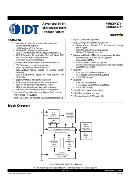
Advanced 64-bit Microprocessors Product Family 79RC64574 ...
Advanced 64-bit Microprocessors Product Family 79RC64574 ...
Advanced 64-bit Microprocessors Product Family 79RC64574 ...

You also want an ePaper? Increase the reach of your titles
YUMPU automatically turns print PDFs into web optimized ePapers that Google loves.
79RC<strong>64</strong>574 79RC<strong>64</strong>575ferring data between the processor and memory at a peak rate of1000MB/sec. A boot-time selectable option to run the system interfaceas 32-<strong>bit</strong>s wide—using basically the same protocols as the <strong>64</strong>-<strong>bit</strong>system—is also supported.A boot-time mode control interface initializes fundamentalprocessor modes and is a serial interface that operates at a very lowfrequency (SysClock divided by 256). This low-frequency operationallows the initialization information to be kept in a low-cost EPROM;alternatively, the twenty-or-so <strong>bit</strong>s could be generated by the systeminterface ASIC or a simple PAL. The boot-time serial stream is shown inTable 3.SerialBitDescription0 Reserved Must be set to 0.1:4 Transmit-dat a-pattern.Bit 4 is MSB5:7 PClock-to-SysClk-Ratio.Bit 7 is MSBValue & Mode Setting<strong>64</strong>-<strong>bit</strong> bus width:0: DDDD1: DDxDDx2: DDxxDDxx3: DxDxDxDx4: DDxxxDDxxx5: DDxxxxDDxxxx6: DxxDxxDxxDxx7: DDxxxxxxDDxxxxxx8: DxxxDxxxDxxxDxxx9-15: Reserved . Must not be selecte d.32-<strong>bit</strong> bus width:0: WWWWWWWW1: WWxWWxWWxWWx2: WWxxWWxxWWxxWWxx3: WxWxWxWxWxWxWxWx4: WWxxxWWxxxWWxxxWWxxx5: WWxxxxWWxxxxWWxxxxWWxxxx6: WxxWxxWxxWxxWxxWxxWxxWxx7: WWxxxxxxWWxxxxxxWWxxxxxxWWxxxxxx8: WxxxWxxxWxxxWxxxWxxxWxxxWxxxWxxx9-15: Reserved . Must not be selecte d.0: 21: 32: 43: 54: 65: 76: 87: Rese rved8 Endianness 0: Little endian1: Big endian9:1 0 Non-block writeMode. Bit 10 isMSB00: R4400 compatible01: Reserved10: Pipelin ed-Write-Mode11: Writ e-Re issue-Mod eTable 3 Boot-time Mode Stream (Page 1 of 2)SerialBitDescription11 TimerIntEn Timer inte rru pt se tting s:0: Enable Timer Interrupt on Int(5)1: Disable Timer Interrupt on Int(5)12 System Inte rfaceBus Width.13:14 Drv_OutBit 14 is MSB15:17 Write address towrite d ata delay.Interface bus wid th co ntrol settin gs:0: <strong>64</strong>-<strong>bit</strong> system interface1: 32-<strong>bit</strong> system interfaceSlew rate cont rol of the outp ut drivers:10: 100% strengt h (fastest)11: 83% strength00: 67% strength01: 50% strength (slowest)From 0 to 7 SysClk cycles:0: AD...1: AxD...2: AxxD...3: AxxxD...4: AxxxxD...5: AxxxxxD...6: AxxxxxxD...7: AxxxxxxxD...18 Reserved User must select ‘0’19 Ext endMultip lica tionRepea t Rate.Initial setting of the “Fast Multiply” <strong>bit</strong>.0: Enable Fast Multiply1: Do n ot Enable Fast Multiply20:24 Reserved User must select ‘0’25:26 Systemconfig urationid entif ier.27:256 Reserved User must select ‘0’Value & Mode SettingNote: For pipeline speeds >25 0MHz, this b it mustbe set to ‘1’.Software visible in processorConfig[21:20]0: Con fig[21 :20] = Mo de Bit [2 5:26]Must be set to 0.Table 3 Boot-time Mode Stream (Page 2 of 2)The clocking interface allows the CPU to be easily mated withexternal reference clocks. The CPU input clock is the bus referenceclock and can be between 33 and 125MHz. An on-chip phase-lockedloop(PLL) generates the pipeline clock (PClock) through multiplicationof the system interface clock by values of 2,3,4,5,6,7 or 8, as defined atsystem reset. This allows the pipeline clock to be implemented at asignificantly higher frequency than the system interface clock. TheRC<strong>64</strong>574/575 support both single data (one byte through full CPU buswidth) and 8-word block transfers on the SysAD bus.The RC<strong>64</strong>574/575 implement additional write protocols thatdouble the effective write bandwidth. The write re-iss ue has a repeatrate of 2 cycles per write. Pipelined writes have the same 2-cycle perwrite repeat rate, but can issue an additional write after WrRdy* deasserts.4 of 28 December 14, 2001
79RC<strong>64</strong>574 79RC<strong>64</strong>575Choosing a 32- or <strong>64</strong>-<strong>bit</strong> wide system interface dictates whether acache line block transaction requires 4 double word data cycles or 8single word cyc les as well as whether a single data transfer—larger than4 bytes—must be divided into two smaller transfers.As shown in Table 3, the bus delay can be defined as 0 to 7SysClock cycles and is activated and controlled through mode <strong>bit</strong>(17:15) s ettings selected during the res et initialization sequence. The‘000’ setting provides the same write operations timing protocol as theRC4<strong>64</strong>0, RC4650, and RC5000 processors.To facilitate discrete interface to SyncDRAM, the RC<strong>64</strong>574/575 businterface is enhanced during write cycles with a programmable delaythat is inserted between the write address and the write data (for bothblock and non-block writes).Board-level testing during Run-Time mode is facilitated through thefull JTAG boundary scan facility. Five pins—TDI, TDO, TMS, TCK,TRST*— have been inc orporated to support the standard JTAG interface.The RC<strong>64</strong>574/575 devices offer a direct migration path for designsthat are based on IDT’s RC4<strong>64</strong>0/RC4650 and RC<strong>64</strong>474/RC<strong>64</strong>475processors 2 , through full pin and socket compatibility. Full <strong>64</strong>-<strong>bit</strong>-familysoftware and bus protoc ol compatibility ensures the RC<strong>64</strong>574/575processors access to an existing market and development infrastructure,allowing quicker time to market.Development ToolsAn array of hardware and software tools is available to assist systemdesigners in the rapid development of RC<strong>64</strong>574/575 based systems.This accessibility allows a wide variety of customers to take full advantageof the device’s high-performance features while addressing today’saggressive time-to-market demands.Cache MemoryTo keep the high-performance pipeline of the RC<strong>64</strong>574/575 full andoperating efficiently, on-chip instruction and data caches hav e beenincorporated. Each cache has its own data path and can be accessed inthe same single pipeline clock cycle.The 32kB two-way set associative instruction cache is virtuallyindexed, physically tagged, and word parity protected. Because thiscache is virtually indexed, the virtual-to-physical address translationocc urs in parallel with the cache acc ess, further increasing performanceby allowing both operations to occur simultaneously. The instructioncache provides a peak instruction bandwidth of 2GB/sec at 250MHz.The 32kB two-way set associative data cache is byte parityprotec ted and has a fixed 32-byte (eight words ) line s ize. Its tag isprotected with a single parity <strong>bit</strong>. To allow simultaneous address translationand data c ache ac cess, the D-cache is virtually indexed and physicallytagged. The data cache can provide 8 bytes each clock cycle, for apeak bandwidth of 2GB/s.To lock critical sections of code and/or data into the caches for quickaccess, a per line “cache locking” feature has been implemented.Once enabled, a cache is said to be locked when a particular piece ofcode or data is loaded into the cache and that cache location will not beselected later for refill by other data.Power ManagementExecuting the WAIT instruction enables the processor to enterStandby mode. The internal clocks will shut down, thus freezing thepipeline. The PLL, internal timer, and some of the input pins (Int[5:0]*,NMI*, ExtReq*, Reset*, and ColdReset*) will continue to run. Once inStandby Mode, any interrupt, including the internally generated timerinterrupt, will cause the CPU to exit Standby Mode.Thermal ConsiderationsThe RC<strong>64</strong>574 is packaged in a 128-pin QFP footprint package anduses a 32-<strong>bit</strong> external bus, offering the ideal combination of <strong>64</strong>-<strong>bit</strong>processing power and 32-<strong>bit</strong> low-cost memory systems. The RC<strong>64</strong>575is packaged in a 208-pin QFP footprint package and uses the full <strong>64</strong>-<strong>bit</strong>external bus. The RC<strong>64</strong>575 is ideal for applications requiring <strong>64</strong>-<strong>bit</strong>performance and <strong>64</strong>-<strong>bit</strong> external bandwidth.Both devices are guaranteed in a case temperature range of 0° to+85° C for commercial temperature devices and -40° to +85° C forIndustrial temperature devices. Package type, speed (power) of thedevice, and air flow c onditions affect the equivalent ambient temperatureconditions that will meet thes e specifications .Using the thermal resistance from case to ambient (∅CA) of t hegiven package, the equivalent allowable ambient temperature, TA, canbe calculated. The following equation relates ambient and case temperatures:TA = TC - P * ∅CAwhere P is the maximum power consumption at hot temperature,calculated by using the maximum ICC specification for the device.Typical values for ∅CA at various air flow are shown in Table 4. Notethat the RC<strong>64</strong>574/575 processor implements advanced power management,which substantially reduces the typical power dissipation of thedevice.Revision HistoryJuly 22, 1999: Original data sheet.∅CAAirflow (ft/min) 0 200 400 600 800 10001 28 QFP 16 10 9 7 6 52 08 QFP 20 13 10 9 8 7Table 4 Thermal Resis tance (∅CA) at Various Ai rflows2. To ensure socket compatibility, refer to Table 8 and Table 9.5 of 28 December 14, 2001
79RC<strong>64</strong>574 79RC<strong>64</strong>575September 9, 1999: Made several changes in JTAG Interfacesection of Table 5. Added information on Pin 63 in Table 5.October 14, 1999: Revised data in the Power Consumption tablesfor RC<strong>64</strong>574 and RC<strong>64</strong>575.November 16, 1999: Added Power Curve graphs, revised data inSystem Interface Parameters table, added System Clock Jitter row toClock Parameter table.December 20, 1999: Table 7 “RC<strong>64</strong>574 128-Pin Package” on page12, Changed pin #75 function from Vcc to N.C.March 7, 2000: In Table 1, added “with DSP extensions” in the CPUrow under RC<strong>64</strong>574 and RC<strong>64</strong>575 columns and changed “by set” to “byline” in the Caches row for RC<strong>64</strong>574 and RC<strong>64</strong>575 columns. Addedrows in the Data Output and Data Output Hold rows in the System InterfaceParameters table. Removed references to 300 MHz, and changedbandwidth speed to 2GB/sec ond in Cache Memory section. Rev isedPower Curves.March 28, 2000: Replaced existing figure in Mode ConfigurationInterface Reset Sequence section with 3 reset figures. Revised valuesfor 250MHz in System Interface Parameters table. Changed Data Sheetfrom Preliminary to final.April 3, 2000: Deleted signal t DZ from Figure 6.April 25, 2001: In the Absolute Maximum Ratings table, changedupper voltage limit from 3.8 to 4.0V and removed “Vin should not exceedVcc +0.5 volts” from footnote #1. In DC Electrical Characteristics table,changed maximum value for Vih from 3.3 to 3.8V for all speeds.May 1, 2001: In the Data Output Hold category of the System InterfaceParameters table, changed values in the Min column for all speedsfrom 1.0 to 0. In the Electrical Characteristics table, values were addedto the System Clock Jitter row. Added Industrial temperature range of-40° C to +85° C.December 14, 2001: In Absolute Maximum Ratings Table, changedthe Industrial low-end temperature for symbol Tc to read -40 degreesinstead of 0 degrees.6 of 28 December 14, 2001
79RC<strong>64</strong>574 79RC<strong>64</strong>575Pin Description TableThe following is a list of system interface pins available on the RC<strong>64</strong>574/575. Pin names ending with an asterisk (*) are active when low.Pin Name Type DescriptionSys tem InterfaceExtRqst* I External requestAn e xternal agent asserts ExtRqst* to requ est use of th e System interface . The processor grant s the requestb y asserting Release*.Rele ase* O Release interfaceIn response to the a ssert ion o f ExtRqst* or a CPU read request, the p rocessor asserts Release* and signa lsto the req uesting de vice that the syste m int erface is a vailable .RdRdy* I Read ReadyThe external a gent asserts RdRd y* to indicate that it can accept a processor read req uest .WrRdy* I Write ReadyAn e xternal agent asserts WrRdy* when it can now accept a processor write request.ValidIn* I Vali d InputSignals that an extern al age nt is now d riving a valid ad dress or data o n the SysAD bu s and a valid co mmando r data identifier on the SysCmd bus.ValidOut* O Valid OutputSignals that the processor is now driving a valid addre ss or data on the SysAD bus and a valid co mmand ord ata id entifier on the SysCmd bus.SysAD(63:0) I/O Sys tem address/data busA <strong>64</strong> -<strong>bit</strong> address and d ata bus for communication between the processor and an external agent. In <strong>64</strong> <strong>bit</strong>interface mode, during address phases only, SysAd(35:0 ) contains invalid address in formation. The remainingSysAD(63: 36) pins are n ot used. The whole <strong>64</strong>-<strong>bit</strong> SysAD(63 :0) may be u sed d uring the dat a transferp hase . For all dou ble-word accesse s (read or write), the low-order 3 <strong>bit</strong>s (SysAD[2:0]) will always be out put aszero during the address phase.In 32-<strong>bit</strong> interfa ce mode and in the RC<strong>64</strong>574, SysAD(63:32) is not used, regard less of Endianness. A 3 2-<strong>bit</strong>a ddress and data commu nication between pro cessor an d ext ernal agent is perf ormed via SysAD(31:0).SysADC(7:0) I/O Sys tem address/data check busAn 8 -<strong>bit</strong> bus co ntain ing p arity check <strong>bit</strong>s for the SysAD bus during da ta bus cycles.In 32-<strong>bit</strong> mode and in the RC<strong>64</strong>574, SysADC(7:4) is not used. The SysADC(3:0) contain s check <strong>bit</strong>s forSysAD(31:0).SysCmd(8:0) I/O Sys tem command/data identifier busA 9-<strong>bit</strong> bus for comma nd and data identifier transmission betwee n the processor a nd an externa l age nt.SysCmdP I/O Sys tem Command ParityA single, even-parit y <strong>bit</strong> for the Syscmd bus. This signal is always d riven low.Clock/ Control InterfaceSysClock I SystemClockThe system clock input e stablish es the processo r and bu s op erating frequency. It is multiplied internally by2 ,3,4,5,6,7, or 8 to gen erate th e pip eline clock (PClock).V CCP I Quiet VCC for PLLQuiet VCC for the internal p hase locked loop.V SS P I Quiet V SS for PLLQuiet VSS for the inte rnal phase locked loop.Table 5 Pin Descriptions (Page 1 of 2)7 of 28 December 14, 2001
79RC<strong>64</strong>574 79RC<strong>64</strong>575Pin Name Type DescriptionInterrupt InterfaceInt*(5:0) I InterruptSix general processor int errupts, <strong>bit</strong>-wise ORed with <strong>bit</strong>s 5:0 of the interrupt registe r.NMI* I Non-maskable interruptNon-maskable interrupt, ORed with <strong>bit</strong> 6 of the interrupt register.Initi alization InterfaceV CC Ok I V CC is OKWhe n a ssert ed, this signal in dicates to the processor that the power sup ply has be en above the Vcc minimumfo r more than 10 0 milliseconds and will remain stable. The assertion o f VCCOk initiates the initializationseque nce.ColdReset* I Cold resetThis signal must be asse rted for a power on reset or a cold rese t. ColdReset must be de -asserted synchronouslywith SysClock.Reset* I ResetThis signal must be asserte d for any reset sequence. It can be asserted synchronously or a synchrono usly fora cold reset , or synchronously to initiate a warm reset . Reset must be de-asserted synchronously withSysClock.ModeClock O Boot-mode clockSerial bo ot-mode data clock output at the system clock frequency d ivided by two hun dred fifty-six.ModeIn I Boot-mode data inSerial bo ot-mode data input.JTAG InterfaceTDI I J TAG Data InOn the rising edg e of TCK, se rial input d ata are shifted into either the Instruction re gister or Data reg ister,d epending on the TAP controller state. An external pull-up resistor is required.TDO O J TAG Data OutOn the falling edge of TCK, the TDO is serial data shifted out from eith er the instruction or data register. Whenn o data is shifted out, the TDO is tri-stated (high impedance).TCK I J TAG Clock InputAn input te st clock used to shift into o r out of th e boundary-scan register cells. TCK is inde pendent of the system and proce ssor clock with n omin al 40 -60% duty cycle .TMS I J TAG Command SelectThe logic signal received at the TMS inp ut is decoded by the TAP controller to control test operation. TMS issampled on the rising edge of TCK. An extern al pu ll-up resistor is required.TRST* I J TAG ResetThe TRST* pin is an active-low signal used for asynchron ous reset of the de bug unit, independent o f the processorlogic. During normal CPU op eration, the JTAG controller will be held in the reset mode, asserting thisa ctive low pin.Whe n asserted low, this pin will also tristate the TDO pin. An e xternal pull-down resistor is req uired.JTAG32* I J TAG 32-<strong>bit</strong> scanThis pin is use d to control length of the scan chain for SysAD (32-<strong>bit</strong> or <strong>64</strong>-<strong>bit</strong>) for the JTAG mode. When setto Vss, 32-<strong>bit</strong> b us mode is select ed. In this mode, only SysAD(31:0) a re part of the scan chain. When set toVcc, <strong>64</strong>-<strong>bit</strong> bus mode is selected. In this mo de, SysAD(63:0) a re part of the scan chain. This pin has a b uilt-inp ull-do wn device to guaran tee 32-b it scan, if it is le ft un connected.JR_V cc I JTAG VCCThis pin has an internal pull-down to continuously reset the JTAG contro ller (if left uncon nect ed) bypassingth e TRst* pin. When supplied with Vcc, t he TRst* pin will be the primary control for the JTAG reset.Table 5 Pin Descriptions (Page 2 of 2)8 of 28 December 14, 2001
79RC<strong>64</strong>574 79RC<strong>64</strong>575Logic Diagram — RC<strong>64</strong>574/RC<strong>64</strong>575Figure 1 illustrates the direction and functional groupings for the processor signals.Clock/Control InterfaceJTAG InterfaceSysClockV CCPV SSPTDITDOTMSTRST*TCKJTag32*JR_VccRdRdy*WrRdy*Ex tRqst*RC<strong>64</strong>574/RC<strong>64</strong>575LogicSymbol<strong>64</strong>896SysAD(63:0)SysADC(7:0)SysCmd(8:0)SysCmdPVCCOKColdReset*Reset*ModeClockModeInNMI*Int*(5:0)Interrupt InitializationSystem InterfaceInterfaceInterfaceHandshakeSignalsRelease*ValidIn*ValidOut*Figure 1 Logic Sy mbol for RC<strong>64</strong>574/RC<strong>64</strong>5759 of 28 December 14, 2001
79RC<strong>64</strong>574 79RC<strong>64</strong>575RC<strong>64</strong>575 208-pin QFP Package Pin-outPin names followed by an asterisk (*) are active when low. For maximum flexibility and compatibility with future designs, N.C. pins should be leftfloating.Pin Function Pin Function Pin Function Pin Function1 N.C. 53 JTAG32* 105 N.C. 157 N.C.2 N.C. 54 N.C. 106 N.C. 158 N.C.3 N.C. 55 N.C. 107 N.C. 159 SysAD594 N.C. 56 N.C. 108 N.C. 160 ColdReset*5 N.C. 57 SysCmd 2 109 N.C. 161 SysAD286 N.C. 58 SysAD36 110 N.C. 162 V cc7 N.C. 59 SysAD4 111 N.C. 163 V ss8 N.C. 60 SysCmd 1 112 N.C. 1<strong>64</strong> SysAD609 N.C. 61 V ss 113 N.C. 165 Reset*10 SysAD11 62 V cc 114 SysAD52 166 SysAD2911 V ss 63 SysAD35 115 ExtRqst* 167 SysAD6112 V cc <strong>64</strong> SysAD3 116 V cc 168 SysAD3013 SysCmd 8 65 SysCmd 0 117 V ss 169 V cc14 SysAD42 66 SysAD34 118 SysAD21 170 V ss15 SysAD10 67 V ss 119 SysAD53 171 SysAD6216 SysCmd 7 68 V cc 120 RdRd y* 172 SysAD3117 V ss 69 SysAD2 121 Modein 173 SysAD6318 V cc 70 Int5* 122 SysAD22 174 V cc19 SysAD41 71 SysAD33 123 SysAD54 175 V ss20 SysAD9 72 SysAD1 124 V cc 176 V cc OK21 SysCmd 6 73 V ss 125 V ss 177 SysADC322 SysAD40 74 V cc 126 Release* 178 SysADC723 V ss 75 Int4* 127 SysAD23 179 N.C.24 V cc 76 SysAD32 128 SysAD55 180 TDI25 SysAD8 77 SysAD0 129 NMI* 181 TRst*26 SysCmd 5 78 Int3* 130 V cc 182 TCK27 SysADC4 79 V ss 131 V ss 183 TMS28 SysADC0 80 V cc 132 SysADC2 184 TDO29 V ss 81 Int2* 133 SysADC6 185 V cc P30 V cc 82 SysAD16 134 SysAD24 186 V ss P31 SysCmd 4 83 SysAD48 135 V cc 187 SysClock32 SysAD39 84 Int1* 136 V ss 188 V cc33 SysAD7 85 V ss 137 SysAD56 189 V ssTabl e 6 RC<strong>64</strong>575 208-pin QFP Package Pin-Out (Page 1 of 2)10 of 28 December 14, 2001
79RC<strong>64</strong>574 79RC<strong>64</strong>575Pin Function Pin Function Pin Function Pin Function34 SysCmd 3 86 V cc 138 SysAD25 190 SysADC535 V ss 87 SysAD17 139 SysAD57 191 SysADC136 V cc 88 SysAD49 140 V cc 192 V cc37 SysAD38 89 Int0* 141 V ss 193 V ss38 SysAD6 90 SysAD18 142 N.C 194 SysAD4739 ModeClock 91 V ss 143 SysAD26 195 SysAD1540 WrRd y* 92 V cc 144 SysAD58 196 SysAD4<strong>64</strong>1 SysAD37 93 SysAD50 145 N.C. 197 V cc42 SysAD5 94 ValidIn* 146 V cc 198 V ss43 V ss 95 SysAD19 147 V ss 199 SysAD1444 V cc 96 SysAD51 148 SysAD27 200 SysAD4545 N.C. 97 V ss 149 N.C. 201 SysAD1346 N.C. 98 V cc 150 JR_V cc 202 SysAD4447 N.C. 99 ValidOut* 151 N.C. 203 V ss48 N.C. 100 SysAD20 152 N.C. 204 V cc49 N.C. 101 N.C. 153 N.C. 205 SysAD1250 N.C. 102 N.C. 154 N.C. 206 SysCmd P51 N.C. 103 N.C. 155 N.C. 207 SysAD4352 N.C. 104 N.C. 156 N.C. 208 N.C.Tabl e 6 RC<strong>64</strong>575 208-pin QFP Package Pin-Out (Page 2 of 2)11 of 28 December 14, 2001
79RC<strong>64</strong>574 79RC<strong>64</strong>575RC<strong>64</strong>574 128-pin Package Pin-outN.C. pins should be left floating for maximum flexibility as well as for compatibility with future designs. An asterisk (*) identifies a pin that is activewhen low.Pin Function Pin Function Pin Function Pin Function1 JTAG32* 33 V cc 65 V cc 97 V cc2 SysCmd2 34 V ss 66 SysAD28 98 V ss3 V cc 35 SysAD13 67 ColdReset* 99 SysAD194 V ss 36 SysAD14 68 SysAD27 100 ValidIn*5 SysAD5 37 V ss 69 V ss 101 V cc6 WrRdy* 38 V cc 70 V cc 102 V ss7 Mo deClock 39 SysAD15 71 JR_V cc 103 SysAD188 SysAD6 40 V ss 72 SysAD26 104 Int0*9 V cc 41 V cc 73 N.C. 105 SysAD1710 V ss 42 SysADC1 74 V ss 106 V cc11 SysCmd3 43 V ss 75 N.C. 107 V ss12 SysAD7 44 V cc 76 SysAD25 108 Int1*13 SysCmd4 45 SysClock 77 V ss 109 SysAD1614 V cc 46 V ss P 78 V cc 110 Int2*15 V ss 47 V cc P 79 SysAD24 111 V cc16 SysADC0 48 TDO 80 SysADC2 112 V ss17 SysCmd5 49 TMS 81 V ss 113 Int3*18 SysAD8 50 TCK 82 V cc 114 SysAD019 V cc 51 TRst* 83 NMI* 115 Int4*20 V ss 52 TDI 84 SysAD23 116 V cc21 SysCmd6 53 V ss 85 Release* 117 V ss22 SysAD9 54 SysADC3 86 V ss 118 SysAD123 V cc 55 V cc OK 87 V cc 119 Int5*24 V ss 56 V ss 88 SysAD22 120 SysAD225 SysCmd7 57 Vcc 89 Modein 121 V cc26 SysAD10 58 SysAD31 90 RdRd y* 122 V ss27 SysCmd8 59 V ss 91 SysAD21 123 SysCmd028 V cc 60 V cc 92 V ss 124 SysAD329 V ss 61 SysAD30 93 V cc 125 V cc30 SysAD11 62 SysAD29 94 ExtRqst* 126 V ss31 SysCmdP 63 Rese t* 95 SysAD20 127 SysCmd132 SysAD12 <strong>64</strong> V ss 96 ValidOut* 128 SysAD4Table 7 RC<strong>64</strong>574 128-Pin Package12 of 28 December 14, 2001
79RC<strong>64</strong>574 79RC<strong>64</strong>575RC<strong>64</strong>574 Socket Compatibility to RC<strong>64</strong>474 & RC4<strong>64</strong>0The RC<strong>64</strong>574/575 is 100% pin compatible with the RC<strong>64</strong>474/475 with the supply voltage being the only difference. RC<strong>64</strong>474/475 requires a 3.3Vsupply, while RC<strong>64</strong>574/575 requires a 2.5V supply.To ensure socket compatibility between the RC<strong>64</strong>574/RC<strong>64</strong>474 and the RC4<strong>64</strong>0 devices, several pin changes are required, as shown in the tablesbelow. Note: The RC<strong>64</strong>574/575 are 2.5V parts and as such all Vcc must be at the correct voltage for a given part.PinRC4<strong>64</strong>0RC<strong>64</strong>574/RC<strong>64</strong>474Compatible toRV4<strong>64</strong>0?Comments1 N.C JTAG32 * Yes Pin h as an internal pull-down, t o enable 32-b it scan.Can also be left a N. C.48 V ss TDO Yes Can be driven with V ss , if JTAG is not need ed. Is tristated whenTR st* is low .49 V ss TMS Yes Can be drive n with V ss if JTAG is not needed .50 V ss TCK Yes Can be drive n with V ss if JTAG is not needed .51 V ss TRst* Yes Can be drive n with V ss if JTAG is not needed .52 V ss TDI Yes Can be drive n with V ss if JTAG is not needed .71 N.C. JR_V cc Yes Can be left N.C. in RC<strong>64</strong>574, if JTAG is not need. If JTAG isneeded, it must be d riven to V cc .Table 8 RC<strong>64</strong>574 Socket Compati bility to RC<strong>64</strong>474 and R4<strong>64</strong>0RC<strong>64</strong>575 Socket Compatibility to RC<strong>64</strong>475 & RC4650PinRV465032-<strong>bit</strong>RC<strong>64</strong>57532-<strong>bit</strong>RC<strong>64</strong>47532-<strong>bit</strong>RV4650<strong>64</strong>-<strong>bit</strong>RC<strong>64</strong>575<strong>64</strong>-<strong>bit</strong>RC<strong>64</strong>475<strong>64</strong>-<strong>bit</strong>Compatible toRV4650?Comments53 N.C. JTAG32* No Connect JTAG32* Yes In 32-<strong>bit</strong>, this pin can be left unconnectedbecause of internal p ull-d own.In <strong>64</strong>-<strong>bit</strong>, this assumes that JTAG willnot be used . If using JTAG, th is pinmust be at V cc .150 N.C. JR_V cc No Connect JR_V cc Yes In RC<strong>64</strong>475, can be left a N.C, ifJTAG is not need. If JTAG is n eeded,it must be driven to V cc .180 N.C. TDI No Connect TDO Yes If JTAG is no t needed, can be left aN.C.181 N.C. TRsT* No Connect TRsT* Yes If JTAG is no t needed, can be left aN.C.182 N.C. TCK No Connect TCK Yes If JTAG is no t needed, can be left aN.C.183 N.C. TMS No Connect TMS Yes If JTAG is no t needed, can be left aN.C.184 N.C. TDO No Connect TDIO Yes If JTAG is no t needed, can be left aN.C.Tabl e 9 RC<strong>64</strong>575 Soc ket Compatibility to RC<strong>64</strong>475 & RC465013 of 28 December 14, 2001
79RC<strong>64</strong>574 79RC<strong>64</strong>575Absolute Maximum RatingsNote: Stresses greater than those listed under ABSOLUTE MAXIMUM RATINGS may cause permanent damage to the device. This is astress rating only and functional operation of the device at these or any other conditions above those indicated in the operational sections ofthis specification is not implied. Exposure to absolute maximum rating conditions for extended periods may affect reliability.Symbol Rating Commercial (2.5V±5%) Industrial (2.5V±5%) UnitV TERM Terminal Voltage with respect to GND –0.5 1 to +4.01. V In minimum = –2.0V for pulse width less than 15ns. For 3.3V tolerant input, V In maximum is 3.8V.–0.5 1 t o +4.0 VT C Op erating Temperature (case) 0 to +85 -40 to +8 5 °CT BIAS2Case Te mperat ure Under Bias –5 5 to +125 –5 5 to +125 °CT STG Storage Tempe rature –5 5 to +125 –5 5 to +125 °CI IN DC In put Current 20 3I OUT DC Outpu t Current 50 42. Case temperature when device is powered up but not operating.3. When V IN < 0V or V IN > V CC .4. Not more than one output should be shorted at a time. Duration of the short should not exceed 30 seconds.20 3 mA50 4 mARecommended Operation Temperature and Supply VoltageGrade Temperature GNDRC<strong>64</strong>574/575VccDC Electrical CharacteristicsComm ercia l 0°C to +85°C (Case) 0V 2.5V±5%Industrial -40°C to + 85°C (Ca se) 0V 2.5V±5%Commercial Temperature Range—RC<strong>64</strong>574/575(T case= 0°C to +85°C Commercial, T case= -40°C to +85°C Industrial, V cc= 2.5V± 5%)ParameterRC<strong>64</strong>574/RC<strong>64</strong>575200MHzRC<strong>64</strong>574/RC<strong>64</strong>575250MHzMin Max Min MaxConditionsV OL — 0.1V — 0.1V |IOUT|= 20uAV OH V cc - 0.1 V — V cc - 0.1V —V OL — 0.4V — 0.4V |IOUT|= 4mAV OH 2.0V — 2.0V —V IL –0.5V 0.2V cc –0.5V 0.2V cc —V IH 0.7 V cc 3.8V 0.7 V cc 3.8V —I IN — ±10uA — ±10uA 0 ≤ VIN ≤ VCCC IN — 10pF — 10pF —14 of 28 December 14, 2001
79RC<strong>64</strong>574 79RC<strong>64</strong>575ParameterRC<strong>64</strong>574/RC<strong>64</strong>575200MHzRC<strong>64</strong>574/RC<strong>64</strong>575250MHzMin Max Min MaxConditionsC IO — 10pF — 10pF —C cl k — 10pF — 10pFI/O LEAK — 20uA — 20uA Input/Output L eaka gePower Consumption—RC<strong>64</strong>574Note: The following table ass umes as 4:1 pipeline to bus clock ratio.ParameterRC<strong>64</strong>574 200MHzTypical 1I CC stand-by — 60 mA 21. Typic al integer ins truc tion mix and cache miss r ates.RC<strong>64</strong>574 250MHzMax Typical 1 Max— 60 mA 2 C L = 0pF 3Conditions2. These are not tested. They are the results of engineering analysis and are provided for reference only.3. Guaranteed by design.— 120 mA 2 — 120 mA 2 C L = 50pFactive 470 mA 2 55 0 mA 2 550 mA 2 680 mA 2 C L = 0pFNo SysAd activity 3Vcc = 2.63V550mA 2 65 0 mA 2 650 mA 2 800 mA 2 C L = 50pFR4x00 compatible writes,T C = 25 o CVcc = 2.63V600 mA 2 71 5 mA 44. These are the specifications IDT tests to insure compliance.715 mA 2 880 mA 4 C L = 50pFPipelined writes or writere-issue,T C = 25 o C 3Vcc = 2.63VRC<strong>64</strong>574 Power CurvesThe following two graphs contain power curves that show power consumption at various bus frequencies. Power consumption is based on thevalues for R4x00 compatible write mode, shown in the table above.Note: Only pipeline frequencies that are integer multiples (2x, 3x, etc.) of bus frequencies are supported.15 of 28 December 14, 2001
79RC<strong>64</strong>574 79RC<strong>64</strong>575Typical Power (mA)10009003x 2x8005x 4x7006006x7x50040030020010020 40 60 80 100 120System Bus Speed (MHz)2x Mode3x Mode4x Mode5x Mode6x Mode7x ModeFigure 2 Typical Power Usage - RC<strong>64</strong>574Maximum Power (mA)110010003x2x9005x8004x6x700 7x60050040030020020 40 60 80 100 120System Bus Speed (MHz)2x Mode3x Mode4x Mode5x Mode6x Mode7x ModeFigure 3 Maximum Power Usage - RC<strong>64</strong>57416 of 28 December 14, 2001
79RC<strong>64</strong>574 79RC<strong>64</strong>575Power Consumption—RC<strong>64</strong>575Note: The following table ass umes a 4:1 pipeline to bus clock ratio.ParameterRC<strong>64</strong>575 200MHzTypical 1I CC sta nd-by — 60 mA 2act ive,<strong>64</strong>-<strong>bit</strong>busoption 41. Typic al integer instruction mix and cache miss rates.RC<strong>64</strong>575 250MHzMax Typical 1 Max— 60 mA 2 C L = 0pF 32. These are not tested. They are the results of engineering analysis and are provided for reference only.3. Guaranteed by design.— 120 m 2 A — 120 m 2 A C L = 50pF4. In 32-<strong>bit</strong> bus option, use RC<strong>64</strong>574 power consumption values.Conditions510 mA 2 680 mA 2 600 mA 2 810 mA 2 C L = 0pFNo SysAd activity 3Vcc = 2.63V60 0 mA 2 800 mA 2 70 0 mA 2 950 mA 2 C L = 50pFR4 x00 compa tible writes,T C = 25 o CVcc = 2.63V660 mA 2 880 mA 55. These are the specifications IDT tests to insure compliance.770 mA 2 1050 mA 5 C L = 50pFPipelined writes or write re -issue,T C = 25 o C 3Vcc = 2.63VRC<strong>64</strong>575 Power CurvesThe following two graphs contain power curves that show power consumption at various bus frequencies. Power consumption is based on thevalues for R4x00 compatible write mode, shown in the table above.Note: Only pipeline frequencies that are integer multiples (2x, 3x, etc.) of bus frequencies are supported.Typical Power (mA)11009007005003007x6x5x4x3x2x2x Mode3x Mode4x Mode5x Mode6x Mode7x Mode10020 40 60 80 100 120System Bus Speed (MHz)Figure 4 Typical Power Usage - RC<strong>64</strong>57517 of 28 December 14, 2001
79RC<strong>64</strong>574 79RC<strong>64</strong>5751400Maximum Power (mA)12005x 3x 2x10007x 6x4x80060040020020 40 60 80 100 120System Bus Speed (MHz)2x Mode3x Mode4x Mode5x Mode6x Mode7x ModeFigure 5 Maximum Power Usage - RC<strong>64</strong>57518 of 28 December 14, 2001
79RC<strong>64</strong>574 79RC<strong>64</strong>575Timing Characteristics—RC<strong>64</strong>574/RC<strong>64</strong>575Cycle 1 2 3 4SysClockt SysClkt SysClkLowt SysClkPSysAD,SysCmd Driven D D DSysADCt DOt DOHSysAD,SysCmd Received D D D DSysADCt DSt DHControl Signal CPU drivenValidOut*Release*t DOt DOHControl Signal CPU receivedRdRdy*WrRdy*ExtRqst*ValidIn*NMI*Int*(5:0)t DSt DH* = acti ve lo w si gnalFigure 6 System Clocks Data Setup, Output, and Hold Timingt TCKTCKt3t1t5t2TDI/TMSt DSTDO TDO TDOt DHt DOt4Notes to diagram:t1 = t TCKlowt2 = t TCKHIGHTRST*t3 = t TCKFALLt4 = T RST (reset pulse width)t5 = t TCKRise> = 25 nsFigure 7 Standard JTAG Timing19 of 28 December 14, 2001
79RC<strong>64</strong>574 79RC<strong>64</strong>575System Interface ParametersParameterSymbolTestConditionsRC<strong>64</strong>574/RC<strong>64</strong>575200MHzRC<strong>64</strong>574/RC<strong>64</strong>575250MHzUnitsMin Max Min MaxData Output t DO = Max mode 14 ..13 = 10(Faste st)mode 14 ..13 = 11(85%)mode 14 ..13 = 00(66%)— 5 — 4.3 ns— 6 — 4.5 ns— 7 — 5 nsData Output Hold t DOH1Data Input1. 50 pf loading on external output signalsBoot-time Interface Parametersmode 14 ..13 = 01(Slowest)— 8 — 5 nsmode 14 ..13 = 10 0 — 0 — nsmode 14 ..13 = 11 0 — 0 — nsmode 14 ..13 = 00 0 — 0 — nsmode 14 ..13 = 01 0 — 0 — nst DSt rise = 3ns2 — 2 — nst DHt fa ll = 3ns1.0 — 1.0 — nsParameterSymbolTestConditionsRC<strong>64</strong>574/RC<strong>64</strong>575200MHzRC<strong>64</strong>574/RC<strong>64</strong>575250MHzConditionsMin Max Min MaxMode Data Setup t DS — 4 — 4 — SysClock CycleMode Data Hold t DH — 0 — 0 — SysClock Cycle20 of 28 December 14, 2001
79RC<strong>64</strong>574 79RC<strong>64</strong>575Mode Configuration Interface Reset SequenceVcc2.3V2.3VMasterClock(MClk)VCCOK> 100msTDS256 MClk cycles256MClkcyclesModeClockModeInTDSTMDSBit 0TMDHBitBit 1255TDSColdReset*TDS> <strong>64</strong>K MClk cycles> <strong>64</strong> MClk cyclesTDSReset*Figure 8 Power-on ResetVccMasterClock(MClk)VCCOKTDS> 100msTDS256 MClk cycles256MClkcyclesModeClockModeInTMDSTMDHBit Bit Bit0 1 255TDSTDSColdReset*TDS> <strong>64</strong>K MClk cycles> <strong>64</strong> MClk cyclesTDSReset*Figure 9 Cold ResetVccMasterClock(MClk)VCCOK256 MClk cyclesModeClockModeInColdReset*TDSTDSReset*> <strong>64</strong> MClk cyclesFigure 10 Warm Reset21 of 28 December 14, 2001
79RC<strong>64</strong>574 79RC<strong>64</strong>575AC Electrical Characteristics(T case= 0°C to +85°C Commercial, T case= -40°C to +85°C Industrial, V cc= 2.5V± 5%)Clock Parameters—RC<strong>64</strong>574/575ParameterSymbolTestConditionsRC<strong>64</strong>574/RC<strong>64</strong>575200MHzRC<strong>64</strong>574/RC<strong>64</strong>575250MHzMin Max Min MaxUnitsPipe line Clock Frequency PCLk — 100 200 100 250 MHzSystem Clock HIGH t SCHIGH Transition ≤ 3ns 3 — 3 — nsSystem Clock LOW t SCLOW Transition ≤ 3ns 3 — 3 — nsSystem Clock Frequency — — 33 100 33 125 MHzSystem Clock Period t SCP — 10 30 8 30 nsSystem Clock Jitter t JITTER — — + 25 0 — + 250 psSystem Clock Rise Time 1t SCRise — — 2 — 2 nsSystem Clock Fall Time 1 t SCFall — — 2 — 2 nsModeClock Period t Mo deCKP — — 256 t SCP — 256 t SCP nsJTAG Clock Inpu t Period t TCK — — 100 — 100 nsJTAG Clock HIGH t TCKHIGH — — 40 — 40 nsJTAG Clock Low t TCKLOW — — 40 — 40 nsJTAG Clock Rise Time t TCKRise — — 5 — 5 nsJTAG Clock Fall Time t TCKFall — — 5 — 5 ns1. Rise and Fall times are measured between 10% and 90%Capacitive Load Deration—RC<strong>64</strong>574/575ParameterSymbolTestConditions200MHz250MHzMin Max Min MaxUnitsLoad Derate C LD — — 2 — 2 ns/25pFOutput Loading for AC TestingV REF+1.5V–+To D eviceUnder TestC LDSignalCldAll Signals50 pF22 of 28 December 14, 2001
79RC<strong>64</strong>574 79RC<strong>64</strong>575RC<strong>64</strong>575 208-pin Package DiagramThe RC<strong>64</strong>575 is available in a 208-pin QFP package.23 of 28 December 14, 2001
79RC<strong>64</strong>574 79RC<strong>64</strong>575RC<strong>64</strong>575 208-pin Package Diagram (page2)24 of 28 December 14, 2001
79RC<strong>64</strong>574 79RC<strong>64</strong>575RC<strong>64</strong>574 128-pin Package Diagram (page 1 of 3)The RC<strong>64</strong>574 is available in a 128-pin QFP package.25 of 28 December 14, 2001
79RC<strong>64</strong>574 79RC<strong>64</strong>575RC<strong>64</strong>574 128-pin Package Diagram (page 2 of 3)326 of 28 December 14, 2001
79RC<strong>64</strong>574 79RC<strong>64</strong>575RC<strong>64</strong>574 128-pin Package Diagram (page 3 of 3)27 of 28 December 14, 2001
79RC<strong>64</strong>574 79RC<strong>64</strong>575Ordering InformationIDT79RCXX YY XXXX 999 A A<strong>Product</strong>TypeOperatingVoltageDeviceTypeSpeed Package Temp range/ProcessBlankIDZDPCommercial Temperature(0° C t o +85° C Case)Industrial Temperature(-40°C to +85° C Case)128-pin QFP208-pin QFP200250200 MHz Pipeline Clk250 MHz Pipeline Clk574575Embedded ProcessorT79RC<strong>64</strong>2.5V +/-5%<strong>64</strong>-<strong>bit</strong> EmbeddedMicroprocessorValid CombinationsIDT79RC6 4T574 - 200, 25 0, DZIDT79RC6 4T575 - 200 , 25 0, DPIDT79RC6 4T574 - 200, 25 0, DZIIDT79RC6 4T575 - 200, 25 0, DPI128-p in QFP package, Commercial Temperatu re208-p in QFP package, Commercial Temperatu re128-p in QFP package, Industrial Temperature08-pin QFP p ackage, In dust rial TemperatureCORPORATE HEADQUARTERS2975 Stender WaySanta Clara, CA 95054for SALES:800-345-7015 or 408-727-6116fax: 408-330-1748www.idt.comfor Tech Support:email: rischelp@idt.comphone: 408-492-820828 of 28 December 14, 2001


