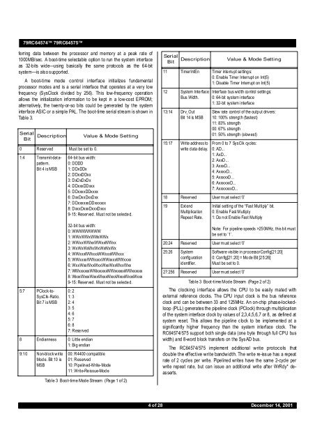
79RC<strong>64</strong>574 79RC<strong>64</strong>575ferring data between the processor and memory at a peak rate of1000MB/sec. A boot-time selectable option to run the system interfaceas 32-<strong>bit</strong>s wide—using basically the same protocols as the <strong>64</strong>-<strong>bit</strong>system—is also supported.A boot-time mode control interface initializes fundamentalprocessor modes and is a serial interface that operates at a very lowfrequency (SysClock divided by 256). This low-frequency operationallows the initialization information to be kept in a low-cost EPROM;alternatively, the twenty-or-so <strong>bit</strong>s could be generated by the systeminterface ASIC or a simple PAL. The boot-time serial stream is shown inTable 3.SerialBitDescription0 Reserved Must be set to 0.1:4 Transmit-dat a-pattern.Bit 4 is MSB5:7 PClock-to-SysClk-Ratio.Bit 7 is MSBValue & Mode Setting<strong>64</strong>-<strong>bit</strong> bus width:0: DDDD1: DDxDDx2: DDxxDDxx3: DxDxDxDx4: DDxxxDDxxx5: DDxxxxDDxxxx6: DxxDxxDxxDxx7: DDxxxxxxDDxxxxxx8: DxxxDxxxDxxxDxxx9-15: Reserved . Must not be selecte d.32-<strong>bit</strong> bus width:0: WWWWWWWW1: WWxWWxWWxWWx2: WWxxWWxxWWxxWWxx3: WxWxWxWxWxWxWxWx4: WWxxxWWxxxWWxxxWWxxx5: WWxxxxWWxxxxWWxxxxWWxxxx6: WxxWxxWxxWxxWxxWxxWxxWxx7: WWxxxxxxWWxxxxxxWWxxxxxxWWxxxxxx8: WxxxWxxxWxxxWxxxWxxxWxxxWxxxWxxx9-15: Reserved . Must not be selecte d.0: 21: 32: 43: 54: 65: 76: 87: Rese rved8 Endianness 0: Little endian1: Big endian9:1 0 Non-block writeMode. Bit 10 isMSB00: R4400 compatible01: Reserved10: Pipelin ed-Write-Mode11: Writ e-Re issue-Mod eTable 3 Boot-time Mode Stream (Page 1 of 2)SerialBitDescription11 TimerIntEn Timer inte rru pt se tting s:0: Enable Timer Interrupt on Int(5)1: Disable Timer Interrupt on Int(5)12 System Inte rfaceBus Width.13:14 Drv_OutBit 14 is MSB15:17 Write address towrite d ata delay.Interface bus wid th co ntrol settin gs:0: <strong>64</strong>-<strong>bit</strong> system interface1: 32-<strong>bit</strong> system interfaceSlew rate cont rol of the outp ut drivers:10: 100% strengt h (fastest)11: 83% strength00: 67% strength01: 50% strength (slowest)From 0 to 7 SysClk cycles:0: AD...1: AxD...2: AxxD...3: AxxxD...4: AxxxxD...5: AxxxxxD...6: AxxxxxxD...7: AxxxxxxxD...18 Reserved User must select ‘0’19 Ext endMultip lica tionRepea t Rate.Initial setting of the “Fast Multiply” <strong>bit</strong>.0: Enable Fast Multiply1: Do n ot Enable Fast Multiply20:24 Reserved User must select ‘0’25:26 Systemconfig urationid entif ier.27:256 Reserved User must select ‘0’Value & Mode SettingNote: For pipeline speeds >25 0MHz, this b it mustbe set to ‘1’.Software visible in processorConfig[21:20]0: Con fig[21 :20] = Mo de Bit [2 5:26]Must be set to 0.Table 3 Boot-time Mode Stream (Page 2 of 2)The clocking interface allows the CPU to be easily mated withexternal reference clocks. The CPU input clock is the bus referenceclock and can be between 33 and 125MHz. An on-chip phase-lockedloop(PLL) generates the pipeline clock (PClock) through multiplicationof the system interface clock by values of 2,3,4,5,6,7 or 8, as defined atsystem reset. This allows the pipeline clock to be implemented at asignificantly higher frequency than the system interface clock. TheRC<strong>64</strong>574/575 support both single data (one byte through full CPU buswidth) and 8-word block transfers on the SysAD bus.The RC<strong>64</strong>574/575 implement additional write protocols thatdouble the effective write bandwidth. The write re-iss ue has a repeatrate of 2 cycles per write. Pipelined writes have the same 2-cycle perwrite repeat rate, but can issue an additional write after WrRdy* deasserts.4 of 28 December 14, 2001
79RC<strong>64</strong>574 79RC<strong>64</strong>575Choosing a 32- or <strong>64</strong>-<strong>bit</strong> wide system interface dictates whether acache line block transaction requires 4 double word data cycles or 8single word cyc les as well as whether a single data transfer—larger than4 bytes—must be divided into two smaller transfers.As shown in Table 3, the bus delay can be defined as 0 to 7SysClock cycles and is activated and controlled through mode <strong>bit</strong>(17:15) s ettings selected during the res et initialization sequence. The‘000’ setting provides the same write operations timing protocol as theRC4<strong>64</strong>0, RC4650, and RC5000 processors.To facilitate discrete interface to SyncDRAM, the RC<strong>64</strong>574/575 businterface is enhanced during write cycles with a programmable delaythat is inserted between the write address and the write data (for bothblock and non-block writes).Board-level testing during Run-Time mode is facilitated through thefull JTAG boundary scan facility. Five pins—TDI, TDO, TMS, TCK,TRST*— have been inc orporated to support the standard JTAG interface.The RC<strong>64</strong>574/575 devices offer a direct migration path for designsthat are based on IDT’s RC4<strong>64</strong>0/RC4650 and RC<strong>64</strong>474/RC<strong>64</strong>475processors 2 , through full pin and socket compatibility. Full <strong>64</strong>-<strong>bit</strong>-familysoftware and bus protoc ol compatibility ensures the RC<strong>64</strong>574/575processors access to an existing market and development infrastructure,allowing quicker time to market.Development ToolsAn array of hardware and software tools is available to assist systemdesigners in the rapid development of RC<strong>64</strong>574/575 based systems.This accessibility allows a wide variety of customers to take full advantageof the device’s high-performance features while addressing today’saggressive time-to-market demands.Cache MemoryTo keep the high-performance pipeline of the RC<strong>64</strong>574/575 full andoperating efficiently, on-chip instruction and data caches hav e beenincorporated. Each cache has its own data path and can be accessed inthe same single pipeline clock cycle.The 32kB two-way set associative instruction cache is virtuallyindexed, physically tagged, and word parity protected. Because thiscache is virtually indexed, the virtual-to-physical address translationocc urs in parallel with the cache acc ess, further increasing performanceby allowing both operations to occur simultaneously. The instructioncache provides a peak instruction bandwidth of 2GB/sec at 250MHz.The 32kB two-way set associative data cache is byte parityprotec ted and has a fixed 32-byte (eight words ) line s ize. Its tag isprotected with a single parity <strong>bit</strong>. To allow simultaneous address translationand data c ache ac cess, the D-cache is virtually indexed and physicallytagged. The data cache can provide 8 bytes each clock cycle, for apeak bandwidth of 2GB/s.To lock critical sections of code and/or data into the caches for quickaccess, a per line “cache locking” feature has been implemented.Once enabled, a cache is said to be locked when a particular piece ofcode or data is loaded into the cache and that cache location will not beselected later for refill by other data.Power ManagementExecuting the WAIT instruction enables the processor to enterStandby mode. The internal clocks will shut down, thus freezing thepipeline. The PLL, internal timer, and some of the input pins (Int[5:0]*,NMI*, ExtReq*, Reset*, and ColdReset*) will continue to run. Once inStandby Mode, any interrupt, including the internally generated timerinterrupt, will cause the CPU to exit Standby Mode.Thermal ConsiderationsThe RC<strong>64</strong>574 is packaged in a 128-pin QFP footprint package anduses a 32-<strong>bit</strong> external bus, offering the ideal combination of <strong>64</strong>-<strong>bit</strong>processing power and 32-<strong>bit</strong> low-cost memory systems. The RC<strong>64</strong>575is packaged in a 208-pin QFP footprint package and uses the full <strong>64</strong>-<strong>bit</strong>external bus. The RC<strong>64</strong>575 is ideal for applications requiring <strong>64</strong>-<strong>bit</strong>performance and <strong>64</strong>-<strong>bit</strong> external bandwidth.Both devices are guaranteed in a case temperature range of 0° to+85° C for commercial temperature devices and -40° to +85° C forIndustrial temperature devices. Package type, speed (power) of thedevice, and air flow c onditions affect the equivalent ambient temperatureconditions that will meet thes e specifications .Using the thermal resistance from case to ambient (∅CA) of t hegiven package, the equivalent allowable ambient temperature, TA, canbe calculated. The following equation relates ambient and case temperatures:TA = TC - P * ∅CAwhere P is the maximum power consumption at hot temperature,calculated by using the maximum ICC specification for the device.Typical values for ∅CA at various air flow are shown in Table 4. Notethat the RC<strong>64</strong>574/575 processor implements advanced power management,which substantially reduces the typical power dissipation of thedevice.Revision HistoryJuly 22, 1999: Original data sheet.∅CAAirflow (ft/min) 0 200 400 600 800 10001 28 QFP 16 10 9 7 6 52 08 QFP 20 13 10 9 8 7Table 4 Thermal Resis tance (∅CA) at Various Ai rflows2. To ensure socket compatibility, refer to Table 8 and Table 9.5 of 28 December 14, 2001