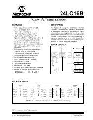
24AA01/02
24AA01/02
24AA01/02

You also want an ePaper? Increase the reach of your titles
YUMPU automatically turns print PDFs into web optimized ePapers that Google loves.
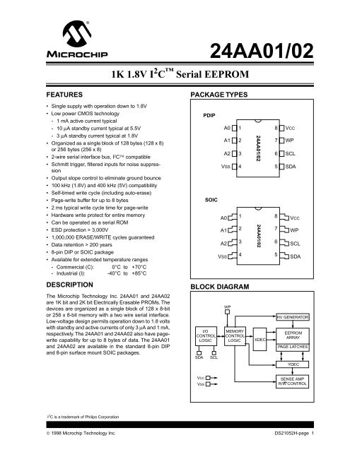
M<strong>24AA01</strong>/<strong>02</strong>1K 1.8V I 2 C Serial EEPROMFEATURESPACKAGE TYPES• Single supply with operation down to 1.8V• Low power CMOS technology- 1 mA active current typical- 10 µA standby current typical at 5.5V- 3 µA standby current typical at 1.8V• Organized as a single block of 128 bytes (128 x 8)or 256 bytes (256 x 8)• 2-wire serial interface bus, I 2 C compatible• Schmitt trigger, filtered inputs for noise suppression• Output slope control to eliminate ground bounce• 100 kHz (1.8V) and 400 kHz (5V) compatibility• Self-timed write cycle (including auto-erase)• Page-write buffer for up to 8 bytes• 2 ms typical write cycle time for page-write• Hardware write protect for entire memory• Can be operated as a serial ROM• ESD protection > 3,000V• 1,000,000 ERASE/WRITE cycles guaranteed• Data retention > 200 years• 8-pin DIP or SOIC package• Available for extended temperature rangesPDIPA0A1A2VSSSOICA0A1A2VSS12341234<strong>24AA01</strong>/<strong>02</strong><strong>24AA01</strong>/<strong>02</strong>87658765VCCWPSCLSDAVCCWPSCLSDA- Commercial (C): 0°C to +70°C- Industrial (I): -40°C to +85°CDESCRIPTIONBLOCK DIAGRAMThe Microchip Technology Inc. <strong>24AA01</strong> and 24AA<strong>02</strong>are 1K bit and 2K bit Electrically Erasable PROMs. Thedevices are organized as a single block of 128 x 8-bitor 256 x 8-bit memory with a two wire serial interface.Low-voltage design permits operation down to 1.8 voltswith standby and active currents of only 3 µA and 1 mA,respectively. The <strong>24AA01</strong> and 24AA<strong>02</strong> also have pagewritecapability for up to 8 bytes of data. The <strong>24AA01</strong>and 24AA<strong>02</strong> are available in the standard 8-pin DIPand 8-pin surface mount SOIC packages.I/OCONTROLLOGICSDASCLWPMEMORYCONTROLLOGICXDECHV GENERATOREEPROMARRAYPAGE LATCHESYDECVCCVSSSENSE AMPR/W CONTROLI 2 C is a trademark of Philips Corporation© 1998 Microchip Technology Inc. DS21052H-page 1
<strong>24AA01</strong>/<strong>02</strong>1.0 ELECTRICALCHARACTERISTICS1.1 Maximum Ratings*VCC...................................................................................7.0VAll inputs and outputs w.r.t. VSS ................-0.6V to VCC +1.0VStorage temperature .....................................-65°C to +150°CAmbient temp. with power applied.............. -65°C to +125°CCSoldering temperature of leads (10 seconds) .............+300°CESD protection on all pins..................................................≥ 4 kV*Notice: Stresses above those listed under “Maximum ratings”may cause permanent damage to the device. This is a stress ratingonly and functional operation of the device at those or anyother conditions above those indicated in the operational listingsof this specification is not implied. Exposure to maximum ratingconditions for extended periods may affect device reliability.TABLE 1-1:NamePIN FUNCTION TABLEFunctionVSSGroundSDASerial Address/Data/I/OSCLSerial ClockWPWrite Protect InputVCC +1.8V to 5.5V Power SupplyA0, A1, A2 No Internal ConnectionTABLE 1-2:DC CHARACTERISTICSVCC = +1.8V to +5.5VCommercial (C):Tamb = 0°C to +70°CIndustrial (I): Tamb = -40°C to +85°CParameter Symbol Min Typ Max Units ConditionsWP, SCL and SDA pins:High level input voltageLow level input voltageHysteresis of Schmitt triggerinputsLow level output voltageVIHVILVHYS.7 VCC—.05 VDDVOL — — .40 VInput leakage current ILI -10 — 10 µA VIN = .1V to 5.5VOutput leakage current ILO -10 — 10 µA VOUT = .1V to 5.5VPin capacitance(all inputs/outputs)Operating currentCIN,COUTICC WriteICC Read————.3 VCC—VVV(Note)IOL = 3.0 mA, VCC = 1.8V— — 10 pF Vcc = 5.0V (Note 1)Tamb = 25˚C, FLCK = 1 MHz————Standby current ICCS ————0.5—0.05Note:This parameter is periodically sampled and not 100% tested.——33—1—10030—mAmAmAmAµAµAµAVCC = 5.5V, SCL = 400 kHzVCC = 1.8V, SCL = 100 kHzVCC = 5.5V, SCL = 400 kHzVCC = 1.8V, SCL = 100 kHzVCC = 5.5V, SDA = SCL = VCCVCC = 3.0V, SDA = SCL = VCCVCC = 1.8V, SDA = SCL = VCCWP = VSSFIGURE 1-1:BUS TIMING START/STOPVHYSSCLSDATSU:STATHD:STATSU:STOSTARTSTOPDS21052H-page 2© 1998 Microchip Technology Inc.
<strong>24AA01</strong>/<strong>02</strong>TABLE 1-3:ParameterAC CHARACTERISTICSSymbolStandard ModeMin Max Min MaxVCC = 4.5 - 5.5VFast Mode Units RemarksClock frequency FCLK — 100 — 400 kHzClock high time THIGH 4000 — 600 — nsClock low time TLOW 4700 — 1300 — nsSDA and SCL rise time TR — 1000 — 300 ns (Note 1)SDA and SCL fall time TF — 300 — 300 ns (Note 1)START condition hold time THD:STA 4000 — 600 — ns After this period the firstclock pulse is generatedSTART condition setuptimeTSU:STA 4700 — 600 — ns Only relevant for repeatedSTART conditionData input hold time THD:DAT 0 — 0 — ns (Note 2)Data input setup time TSU:DAT 250 — 100 — nsSTOP condition setup time TSU:STO 4000 — 600 — nsOutput valid from clock TAA — 3500 — 900 ns (Note2)Bus free time TBUF 4700 — 1300 — ns Time the bus must be freebefore a new transmissioncan startOutput fall time from VIH TOF — 250 20 +0.1 250 ns (Note 1), CB ≤ 100 pFmin to VIL maxCBInput filter spike suppressionTSP — 50 — 50 ns (Note 3)(SDA and SCL pins)Write cycle time TWR — 10 — 10 ms Byte or Page modeEndurance — 1M — 1M — cycles 25°C, Vcc = 5.5V, BlockMode (Note 4)Note 1: Not 100% tested. CB = total capacitance of one bus line in pF.2: As a transmitter, the device must provide an internal minimum delay time to bridge the undefined region(minimum 300 ns) of the falling edge of SCL to avoid unintended generation of START or STOP conditions.3: The combined TSP and VHYS specifications are due to new Schmitt trigger inputs which provide improvednoise spike suppression. This eliminates the need for a TI specification for standard operation.4: This parameter is not tested but guaranteed by characterization. For endurance estimates in a specific application,please consult the Total Endurance Model which can be obtained on our BBS or website.FIGURE 1-2:BUS TIMING DATATFTRTHIGHTLOWSCLSCLINTSU:STATSPTHD:STATHD:DAT TSU:DAT TSU:STOTAATHD:STATAATBUFSDAOUT© 1998 Microchip Technology Inc. DS21052H-page 3
<strong>24AA01</strong>/<strong>02</strong>2.0 FUNCTIONAL DESCRIPTIONThe <strong>24AA01</strong>/<strong>02</strong> supports a bi directional 2-wire busand data transmission protocol. A device that sendsdata onto the bus is defined as transmitter, and adevice receiving data as receiver. The bus has to becontrolled by a master device which generates theserial clock (SCL), controls the bus access, and generatesthe START and STOP conditions, while the<strong>24AA01</strong>/<strong>02</strong> works as slave. Both, master and slave canoperate as transmitter or receiver but the master devicedetermines which mode is activated.3.0 BUS CHARACTERISTICSThe following bus protocol has been defined:• Data transfer may be initiated only when the busis not busy.• During data transfer, the data line must remainstable whenever the clock line is HIGH. Changesin the data line while the clock line is HIGH will beinterpreted as a START or STOP condition.Accordingly, the following bus conditions have beendefined (Figure 3-1).3.1 Bus not Busy (A)Both data and clock lines remain HIGH.3.2 Start Data Transfer (B)A HIGH to LOW transition of the SDA line while theclock (SCL) is HIGH determines a START condition.All commands must be preceded by a START condition.3.3 Stop Data Transfer (C)A LOW to HIGH transition of the SDA line while theclock (SCL) is HIGH determines a STOP condition. Alloperations must be ended with a STOP condition.3.4 Data Valid (D)The state of the data line represents valid data when,after a START condition, the data line is stable for theduration of the HIGH period of the clock signal.The data on the line must be changed during the LOWperiod of the clock signal. There is one clock pulse perbit of data.Each data transfer is initiated with a START conditionand terminated with a STOP condition. The number ofthe data bytes transferred between the START andSTOP conditions is determined by the master deviceand is theoretically unlimited, although only the last 16will be stored when doing a write operation. When anoverwrite does occur it will replace data in a first in firstout fashion.3.5 AcknowledgeEach receiving device, when addressed, is obliged togenerate an acknowledge after the reception of eachbyte. The master device must generate an extra clockpulse which is associated with this acknowledge bit.Note: The <strong>24AA01</strong>/<strong>02</strong> does not generate anyacknowledge bits if an internal programmingcycle is in progress.The device that acknowledges, has to pull down theSDA line during the acknowledge clock pulse in such away that the SDA line is stable LOW during the HIGHperiod of the acknowledge related clock pulse. Ofcourse, setup and hold times must be taken intoaccount. A master must signal an end of data to theslave by not generating an acknowledge bit on the lastbyte that has been clocked out of the slave. In thiscase, the slave must leave the data line HIGH to enablethe master to generate the STOP condition.FIGURE 3-1:DATA TRANSFER SEQUENCE ON THE SERIAL BUSDSCLorMSCL(A) (B) (D) (D) (C) (A)DSCLorMSCLSTARTCONDITIONADDRESS ORACKNOWLEDGEVALIDDATAALLOWEDTO CHANGESTOPCONDITIONDS21052H-page 4© 1998 Microchip Technology Inc.
<strong>24AA01</strong>/<strong>02</strong>3.6 Device AddressThe <strong>24AA01</strong>/<strong>02</strong> are software-compatible with olderdevices such as 24C01A, 24C<strong>02</strong>A, 24LC01, and24LC<strong>02</strong>. A single 24AA<strong>02</strong> can be used in place of two24LC01's, for example, without any modifications tosoftware. The “chip select” portion of the control bytebecomes a don't care.After generating a START condition, the bus mastertransmits the slave address consisting of a 4-bit devicecode (1010) for the <strong>24AA01</strong>/<strong>02</strong>, followed by three don'tcare bits.The eighth bit of slave address determines if the masterdevice wants to read or write to the <strong>24AA01</strong>/<strong>02</strong>(Figure 3-2).The <strong>24AA01</strong>/<strong>02</strong> monitors the bus for its correspondingslave address all the time. It generates an acknowledgebit if the slave address was true and it is not in a programmingmode.OperationFIGURE 3-2:ControlCodeChip SelectCONTROL BYTEALLOCATIONREAD/WRITER/WRead 1010 XXX 1Write 1010 XXX 0STARTX = Don’t careSLAVE ADDRESSR/W1 0 1 0 X X XA4.0 WRITE OPERATION4.1 Byte WriteFollowing the start signal from the master, the devicecode (4 bits), the don't care bits (3 bits), and the R/Wbit which is a logic low is placed onto the bus by themaster transmitter. This indicates to the addressedslave receiver that a byte with a word address will followafter it has generated an acknowledge bit during theninth clock cycle. Therefore the next byte transmitted bythe master is the word address and will be written intothe address pointer of the <strong>24AA01</strong>/<strong>02</strong>. After receivinganother acknowledge signal from the <strong>24AA01</strong>/<strong>02</strong> themaster device will transmit the data word to be writteninto the addressed memory location. The <strong>24AA01</strong>/<strong>02</strong>acknowledges again and the master generates a stopcondition. This initiates the internal write cycle, and duringthis time the <strong>24AA01</strong>/<strong>02</strong> will not generate acknowledgesignals (Figure 4-1).4.2 Page WriteThe write control byte, word address and the first databyte are transmitted to the <strong>24AA01</strong>/<strong>02</strong> in the same wayas in a byte write. But instead of generating a stop conditionthe master transmits up to eight data bytes to the<strong>24AA01</strong>/<strong>02</strong> which are temporarily stored in the on-chippage buffer and will be written into the memory after themaster has transmitted a stop condition. After thereceipt of each word, the three lower order addresspointer bits are internally incremented by one. Thehigher order five bits of the word address remains constant.If the master should transmit more than eightwords prior to generating the stop condition, theaddress counter will roll over and the previouslyreceived data will be overwritten. As with the byte writeoperation, once the stop condition is received an internalwrite cycle will begin (Figure 7-1).Note:Page write operations are limited to writingbytes within a single physical page, regardlessof the number of bytes actually beingwritten. Physical page boundaries start ataddresses that are integer multiples of thepage buffer size (or Ôpage sizeÕ) and end ataddresses that are integer multiples of[page size - 1]. If a page write commandattempts to write across a physical pageboundary, the result is that the data wrapsaround to the beginning of the current page(overwriting data previously stored there),instead of being written to the next page asmight be expected. It is therefore necessaryfor the application software to preventpage write operations that would attempt tocross a page boundary.© 1998 Microchip Technology Inc. DS21052H-page 5
<strong>24AA01</strong>/<strong>02</strong>FIGURE 4-1:BUS ACTIVITYMASTERBYTE WRITESTARTCONTROLBYTEWORDADDRESSDATASTOPSDA LINESPBUS ACTIVITYACKACKACKFIGURE 4-2:BUS ACTIVITYMASTERSDA LINEBUS ACTIVITYPAGE WRITESTARTSCONTROLBYTEACKWORDADDRESS (n) DATA n DATA n + 1 DATA n + 7ACKACKACKACKSTOPPDS21052H-page 6© 1998 Microchip Technology Inc.
<strong>24AA01</strong>/<strong>02</strong>5.0 ACKNOWLEDGE POLLINGSince the device will not acknowledge during a writecycle, this can be used to determine when the cycle iscomplete (this feature can be used to maximize busthroughput). Once the stop condition for a write commandhas been issued from the master, the device initiatesthe internally timed write cycle. ACK polling canbe initiated immediately. This involves the master sendinga start condition followed by the control byte for awrite command (R/W = 0). If the device is still busy withthe write cycle, then no ACK will be returned. If thecycle is complete, then the device will return the ACKand the master can then proceed with the next read orwrite command. See Figure 5-1 for flow diagram.FIGURE 5-1:ACKNOWLEDGE POLLINGFLOWSendWrite CommandSend StopCondition toInitiate Write CycleSend StartSend Control Bytewith R/W = 0Did DeviceAcknowledge(ACK = 0)?YesNextOperation6.0 WRITE PROTECTIONThe <strong>24AA01</strong>/<strong>02</strong> can be used as a serial ROM when theWP pin is connected to VCC. Programming will be inhibitedand the entire memory will be write-protected.No7.0 READ OPERATIONRead operations are initiated in the same way as writeoperations with the exception that the R/W bit of theslave address is set to one. There are three basic typesof read operations: current address read, randomread, and sequential read.7.1 Current Address ReadThe <strong>24AA01</strong>/<strong>02</strong> contains an address counter thatmaintains the address of the last word accessed, internallyincremented by one. Therefore, if the previousaccess (either a read or write operation) was toaddress n, the next current address read operationwould access data from address n + 1. Upon receipt ofthe slave address with R/W bit set to one, the <strong>24AA01</strong>/<strong>02</strong> issues an acknowledge and transmits the eight bitdata word. The master will not acknowledge the transferbut does generate a stop condition and the <strong>24AA01</strong>/<strong>02</strong> discontinues transmission (Figure 7-1).7.2 Random ReadRandom read operations allow the master to accessany memory location in a random manner. To performthis type of read operation, first the word address mustbe set. This is done by sending the word address to the<strong>24AA01</strong>/<strong>02</strong> as part of a write operation. After the wordaddress is sent, the master generates a start conditionfollowing the acknowledge. This terminates the writeoperation, but not before the internal address pointer isset. Then the master issues the control byte again butwith the R/W bit set to a one. The <strong>24AA01</strong>/<strong>02</strong> will thenissue an acknowledge and transmits the eight bit dataword. The master will not acknowledge the transfer butdoes generate a stop condition and the <strong>24AA01</strong>/<strong>02</strong> discontinuestransmission (Figure 7-2).7.3 Sequential ReadSequential reads are initiated in the same way as a randomread except that after the <strong>24AA01</strong>/<strong>02</strong> transmits thefirst data byte, the master issues an acknowledge asopposed to a stop condition in a random read. Thisdirects the <strong>24AA01</strong>/<strong>02</strong> to transmit the next sequentiallyaddressed 8-bit word (Figure 7-3).To provide sequential reads the <strong>24AA01</strong>/<strong>02</strong> contains aninternal address pointer which is incremented by one atthe completion of each operation. This address pointerallows the entire memory contents to be serially readduring one operation.7.4 Noise ProtectionThe <strong>24AA01</strong>/<strong>02</strong> employs a VCC threshold detector circuitwhich disables the internal erase/write logic if theVCC is below 1.5 volts at nominal conditions.The SCL and SDA inputs have Schmitt trigger and filtercircuits which suppress noise spikes to assure properdevice operation even on a noisy bus.© 1998 Microchip Technology Inc. DS21052H-page 7
<strong>24AA01</strong>/<strong>02</strong>FIGURE 7-1:CURRENT ADDRESS READBUS ACTIVITYMASTERSTARTCONTROLBYTEDATA nSTOPSDA LINESPBUS ACTIVITYACKNOACKFIGURE 7-2:RANDOM READBUS ACTIVITYMASTERSDA LINEBUS ACTIVITYSTARTSCONTROLBYTEACKWORDADDRESS (n)ACKSTARTSCONTROLBYTEACKDATA (n)NOACKSTOPPFIGURE 7-3:SEQUENTIAL READBUS ACTIVITYMASTERCONTROLBYTEDATA n DATA n + 1 DATA n + 2 DATA n + XSTOPSDA LINEPBUS ACTIVITYACKACKACKACKNOACK8.0 PIN DESCRIPTIONS8.1 SDA Serial Address/Data Input/OutputThis is a bi-directional pin used to transfer addressesand data into and data out of the device. It is an opendrain terminal, therefore the SDA bus requires a pullupresistor to VCC (typical 10KΩ for 100 kHz, 2K for 400kHz).For normal data transfer SDA is allowed to change onlyduring SCL low. Changes during SCL high arereserved for indicating the START and STOP conditions.8.2 SCL Serial ClockThis input is used to synchronize the data transfer fromand to the device.8.3 WPThis pin must be connected to either VSS or VCC.If tied to VSS, normal memory operation is enabled(read/write the entire memory).If tied to VCC, WRITE operations are inhibited. Theentire memory will be write-protected. Read operationsare not affected.This feature allows the user to use the <strong>24AA01</strong>/<strong>02</strong> as aserial ROM when WP is enabled (tied to VCC).8.4 A0, A1, A2These pins are not used by the <strong>24AA01</strong>/<strong>02</strong>. They maybe left floating or tied to either VSS or VCC.DS21052H-page 8© 1998 Microchip Technology Inc.
<strong>24AA01</strong>/<strong>02</strong>NOTES:© 1998 Microchip Technology Inc. DS21052H-page 9
<strong>24AA01</strong>/<strong>02</strong>NOTES:DS21052H-page 10© 1998 Microchip Technology Inc.
<strong>24AA01</strong>/<strong>02</strong><strong>24AA01</strong>/<strong>02</strong> PRODUCT IDENTIFICATION SYSTEMTo order or obtain information, e.g., on pricing or delivery, refer to the factory or the listed sales office..<strong>24AA01</strong>/<strong>02</strong> — /PPackage:TemperatureRange:P = Plastic DIP (300 mil Body), 8-leadSN = Plastic SOIC (150 mil Body), 8-leadSM = Plastic SOIC (207 mil Body), 8-leadBlank = 0°C to +70°CI = -40°C to +85°CDevice:<strong>24AA01</strong><strong>24AA01</strong>T24AA<strong>02</strong>24AA<strong>02</strong>T1.8V, 1K I 2 C Serial EEPROM1.8V, 1K I 2 C Serial EEPROM (Tape and Reel)1.8V, 2K I 2 C Serial EEPROM1.8V, 2K I 2 C Serial EEPROM (Tape and Reel)Sales and SupportData SheetsProducts supported by a preliminary Data Sheet may have an errata sheet describing minor operational differences and recommendedworkarounds. To determine if an errata sheet exists for a particular device, please contact one of the following:1. Your local Microchip sales office2. The Microchip Corporate Literature Center U.S. FAX: (6<strong>02</strong>) 786-72773. The Microchip Worldwide Site (www.microchip.com)Please specify which device, revision of silicon and Data Sheet (include Literature #) you are using.New Customer Notification SystemRegister on our web site (www.microchip.com/cn) to receive the most current information on our products.© 1998 Microchip Technology Inc. DS21052H-page 11
WORLDWIDE SALES AND SERVICEAMERICASCorporate OfficeMicrochip Technology Inc.2355 West Chandler Blvd.Chandler, AZ 85224-6199Tel: 480-786-7200 Fax: 480-786-7277Technical Support: 480-786-7627Web Address: http://www.microchip.comAtlantaMicrochip Technology Inc.500 Sugar Mill Road, Suite 200BAtlanta, GA 30350Tel: 770-640-0034 Fax: 770-640-0307BostonMicrochip Technology Inc.5 Mount Royal AvenueMarlborough, MA 01752Tel: 508-480-9990 Fax: 508-480-8575ChicagoMicrochip Technology Inc.333 Pierce Road, Suite 180Itasca, IL 60143Tel: 630-285-0071 Fax: 630-285-0075DallasMicrochip Technology Inc.4570 Westgrove Drive, Suite 160Addison, TX 75248Tel: 972-818-7423 Fax: 972-818-2924DaytonMicrochip Technology Inc.Two Prestige Place, Suite 150Miamisburg, OH 45342Tel: 937-291-1654 Fax: 937-291-9175DetroitMicrochip Technology Inc.Tri-Atria Office Building32255 Northwestern Highway, Suite 190Farmington Hills, MI 48334Tel: 248-538-2250 Fax: 248-538-2260Los AngelesMicrochip Technology Inc.18201 Von Karman, Suite 1090Irvine, CA 92612Tel: 949-263-1888 Fax: 949-263-1338New YorkMicrochip Technology Inc.150 Motor Parkway, Suite 2<strong>02</strong>Hauppauge, NY 11788Tel: 631-273-5305 Fax: 631-273-5335San JoseMicrochip Technology Inc.2107 North First Street, Suite 590San Jose, CA 95131Tel: 408-436-7950 Fax: 408-436-7955AMERICAS (continued)TorontoMicrochip Technology Inc.5925 Airport Road, Suite 200Mississauga, Ontario L4V 1W1, CanadaTel: 905-405-6279 Fax: 905-405-6253ASIA/PACIFICHong KongMicrochip Asia PacificUnit 2101, Tower 2Metroplaza223 Hing Fong RoadKwai Fong, N.T., Hong KongTel: 852-2-401-1200 Fax: 852-2-401-3431BeijingMicrochip Technology, BeijingUnit 915, 6 Chaoyangmen Bei DajieDong Erhuan Road, Dongcheng DistrictNew China Hong Kong Manhattan BuildingBeijing 100<strong>02</strong>7 PRCTel: 86-10-85282100 Fax: 86-10-85282104IndiaMicrochip Technology Inc.India Liaison OfficeNo. 6, Legacy, Convent RoadBangalore 560 <strong>02</strong>5, IndiaTel: 91-80-229-0061 Fax: 91-80-229-0062JapanMicrochip Technology Intl. Inc.Benex S-1 6F3-18-20, ShinyokohamaKohoku-Ku, Yokohama-shiKanagawa 222-0033 JapanTel: 81-45-471- 6166 Fax: 81-45-471-6122KoreaMicrochip Technology Korea168-1, Youngbo Bldg. 3 FloorSamsung-Dong, Kangnam-KuSeoul, KoreaTel: 82-2-554-7200 Fax: 82-2-558-5934ShanghaiMicrochip TechnologyRM 406 Shanghai Golden Bridge Bldg.2077 Yan’an Road West, Hong Qiao DistrictShanghai, PRC 200335Tel: 86-21-6275-5700 Fax: 86 21-6275-5060ASIA/PACIFIC (continued)SingaporeMicrochip Technology Singapore Pte Ltd.200 Middle Road#07-<strong>02</strong> Prime CentreSingapore 188980Tel: 65-334-8870 Fax: 65-334-8850Taiwan, R.O.CMicrochip Technology Taiwan10F-1C 207Tung Hua North RoadTaipei, Taiwan, ROCTel: 886-2-2717-7175 Fax: 886-2-2545-0139EUROPEUnited KingdomArizona Microchip Technology Ltd.505 Eskdale RoadWinnersh TriangleWokinghamBerkshire, England RG41 5TUTel: 44 118 921 5858 Fax: 44-118 921-5835DenmarkMicrochip Technology Denmark ApSRegus Business CentreLautrup hoj 1-3Ballerup DK-2750 DenmarkTel: 45 4420 9895 Fax: 45 4420 9910FranceArizona Microchip Technology SARLParc d’Activite du Moulin de Massy43 Rue du Saule TrapuBatiment A - ler Etage91300 Massy, FranceTel: 33-1-69-53-63-20 Fax: 33-1-69-30-90-79GermanyArizona Microchip Technology GmbHGustav-Heinemann-Ring 125D-81739 München, GermanyTel: 49-89-627-144 0 Fax: 49-89-627-144-44ItalyArizona Microchip Technology SRLCentro Direzionale ColleoniPalazzo Taurus 1 V. Le Colleoni 120041 Agrate BrianzaMilan, ItalyTel: 39-039-65791-1 Fax: 39-039-689988311/15/99Microchip received QS-9000 quality systemcertification for its worldwide headquarters,design and wafer fabrication facilities inChandler and Tempe, Arizona in July 1999. TheCompany’s quality system processes andprocedures are QS-9000 compliant for itsPICmicro ® 8-bit MCUs, KEELOQ ® code hoppingdevices, Serial EEPROMs and microperipheralproducts. In addition, Microchip’s qualitysystem for the design and manufacture ofdevelopment systems is ISO 9001 certified.All rights reserved. © 1999 Microchip Technology Incorporated. Printed in the USA. 11/99 Printed on recycled paper.Information contained in this publication regarding device applications and the like is intended for suggestion only and may be superseded by updates. No representation or warranty is given and no liability is assumedby Microchip Technology Incorporated with respect to the accuracy or use of such information, or infringement of patents or other intellectual property rights arising from such use or otherwise. Use of Microchip’s productsas critical components in life support systems is not authorized except with express written approval by Microchip. No licenses are conveyed, implicitly or otherwise, under any intellectual property rights. The Microchiplogo and name are registered trademarks of Microchip Technology Inc. in the U.S.A. and other countries. All rights reserved. All other trademarks mentioned herein are the property of their respective companies.© 1999 Microchip Technology Inc.