24AA01/02
24AA01/02
24AA01/02

You also want an ePaper? Increase the reach of your titles
YUMPU automatically turns print PDFs into web optimized ePapers that Google loves.
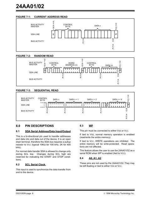
<strong>24AA01</strong>/<strong>02</strong>FIGURE 7-1:CURRENT ADDRESS READBUS ACTIVITYMASTERSTARTCONTROLBYTEDATA nSTOPSDA LINESPBUS ACTIVITYACKNOACKFIGURE 7-2:RANDOM READBUS ACTIVITYMASTERSDA LINEBUS ACTIVITYSTARTSCONTROLBYTEACKWORDADDRESS (n)ACKSTARTSCONTROLBYTEACKDATA (n)NOACKSTOPPFIGURE 7-3:SEQUENTIAL READBUS ACTIVITYMASTERCONTROLBYTEDATA n DATA n + 1 DATA n + 2 DATA n + XSTOPSDA LINEPBUS ACTIVITYACKACKACKACKNOACK8.0 PIN DESCRIPTIONS8.1 SDA Serial Address/Data Input/OutputThis is a bi-directional pin used to transfer addressesand data into and data out of the device. It is an opendrain terminal, therefore the SDA bus requires a pullupresistor to VCC (typical 10KΩ for 100 kHz, 2K for 400kHz).For normal data transfer SDA is allowed to change onlyduring SCL low. Changes during SCL high arereserved for indicating the START and STOP conditions.8.2 SCL Serial ClockThis input is used to synchronize the data transfer fromand to the device.8.3 WPThis pin must be connected to either VSS or VCC.If tied to VSS, normal memory operation is enabled(read/write the entire memory).If tied to VCC, WRITE operations are inhibited. Theentire memory will be write-protected. Read operationsare not affected.This feature allows the user to use the <strong>24AA01</strong>/<strong>02</strong> as aserial ROM when WP is enabled (tied to VCC).8.4 A0, A1, A2These pins are not used by the <strong>24AA01</strong>/<strong>02</strong>. They maybe left floating or tied to either VSS or VCC.DS21052H-page 8© 1998 Microchip Technology Inc.