alpha trx datasheet - RF Solutions
alpha trx datasheet - RF Solutions
alpha trx datasheet - RF Solutions
- No tags were found...

Create successful ePaper yourself
Turn your PDF publications into a flip-book with our unique Google optimized e-Paper software.
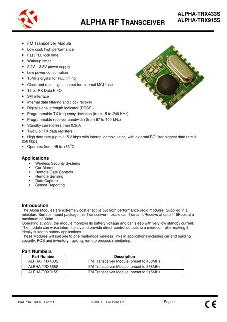
ALPHA <strong>RF</strong> TRANSCEIVERALPHA-TRX433SALPHA-TRX915S• FM Transceiver Module• Low cost, high performance• Fast PLL lock time• Wakeup timer• 2.2V – 3.8V power supply• Low power consumption• 10MHz crystal for PLL timing• Clock and reset signal output for external MCU use• 16 bit RX Data FIFO• SPI interface• Internal data filtering and clock recover• Digital signal strength indicator (DRSSI)• Programmable TX frequency deviation (from 15 to 240 KHz)• Programmable receiver bandwidth (from 67 to 400 kHz)• Standby current less than 0.3uA• Two 8 bit TX data registers• High data rate (up to 115.2 kbps with internal demodulator,with external RC filter highest data rate is256 kbps)• Operates from -45 to +85 O CApplicationsWireless Security SystemsCar AlarmsRemote Gate ControlsRemote SensingData CaptureSensor ReportingIntroductionThe Alpha Modules are extremely cost effective but high performance radio modules. Supplied in aminiature Surface mount package this Transceiver module can Transmit/Receive at upto 115Kbps at amaximum of 300m.Operating at 2-5V, the module monitors its battery voltage and can sleep with very low standby current.The module can wake intermittently and provide direct control outputs to a microcontroller making itideally suited to battery applications.These Modules will suit one to one multi-node wireless links in applications including car and buildingsecurity, POS and inventory tracking, remote process monitoring.Part NumbersPart NumberALPHA-TRX433SALPHA-TRX868SALPHA-TRX915SDescriptionFM Transceiver Module, preset to 433MHzFM Transceiver Module, preset to 868MHzFM Transceiver Module, preset to 915MHzDSALPHA-TRX-6 Feb ‘11 ©2009 <strong>RF</strong> <strong>Solutions</strong> Ltd. Page 1
ALPHA <strong>RF</strong> TRANSCEIVERALPHA-TRX433SALPHA-TRX915SPin Descriptionlow)Pin definition Type Function11 nINT/VDI DI/ DO Interrupt input (active low)/Valid data indicator9 VDD S Positive power supply12 SDI DI SPI data input13 SCK DI SPI clock input8 ANT IN Antenna Connection1 SDO DO Serial data output with bus hold2 nIRQ DO Interrupts request output(activelow)3 FSK/DATA/nFFS DI/DO/DITransmit FSK data input/ Received data output(FIFO not used)/ FIFO select4 DCLK/CFIL/FFIT DO/AIO/DOClock output (no FIFO )/ external filtercapacitor(analog mode)/ FIFO interrupts(activehigh)when FIFO level set to 1, FIFO emptyinterruption can be achieved5 CLK DO Clock output for external microcontroller6 nRES DIO Reset Input (active7, 10 GND S Power ground14 nSEL DI Chip select (active low)DSALPHA-TRX-6 Feb ‘11 ©2009 <strong>RF</strong> <strong>Solutions</strong> Ltd. Page 2
ALPHA <strong>RF</strong> TRANSCEIVERALPHA-TRX433SALPHA-TRX915SMechanical DimensionsElectrical ParametersMaximum (not in working mode)symbol parameter minimum maximum UnitV dd Positive power supply -0.5 6.0 VV in All pin input level -0.5 Vdd+0.5 VI in Input current except power -25 25 mAESD Human body model 1000 VT st Storage temperature -55 125T ld Soldering temperature(10s) 260℃Recommended working rangesymbol parameter minimum maximum UnitV dd Positive power supply 2.2 3.8 VT op Working temperature -40 85℃DSALPHA-TRX-6 Feb ‘11 ©2009 <strong>RF</strong> <strong>Solutions</strong> Ltd. Page 3
ALPHA <strong>RF</strong> TRANSCEIVERALPHA-TRX433SALPHA-TRX915SDC characteristicsymbol parameter Remark minimum typical maximum UnitI dd_TX_0 Supply current433MHz band13mA(TX mode, P out = 0dBm) 915MHz band17I dd_TX_PMAX Supply current433MHz band21mA(TX mode, P out = P max ) 915MHz band25I dd_RX Supply current433MHz band10mA(RX mode)915MHz band13I x Stand by current Crystal and base band3.0 3.5 mAonI pd Sleep mode current All blocks off 0.3 uAI lb Low battery detection 0.5 uAV lb Low battery step 0.1V per step 2.2 5.3 VV lba Low battery detection75 mVaccuracyV il Low level input 0.3*V dd VV ih High level input 0.7*V dd VI il Leakage current V il =0V -1 1 uAI ih Leakage current V ih =V dd , V dd =5.4V -1 1 uAV ol Low level output I ol =2mA 0.4 VV oh High level output I oh =-2mA V dd -0.4 VAC characteristicsymbol parameter remark min typical max Unitf ref PLL frequency 8 10 12 MHzf LOfrequency(10MHz crystalused)433 MHz band,2.5KHz step915 MHz band,7.5KHz step430.24900.72439.75929.27 MHzf LOf LOBWfrequency(8MHZ crystalused)frequency(12MHZ crystalused)Receiverbandwidth433 MHz band,2.5KHz step915 MHz band,7.5KHz step433 MHz band,2.5KHz step915 MHz band,7.5KHz step123456344.19720.573516.281080.86012018024030036067134200270350400351.80743.41 MHz527.711115.1 MHz75150225300375450t lock PLL lock time After 10MHz step hopping,20 usfrequency error
ALPHA <strong>RF</strong> TRANSCEIVERALPHA-TRX433SALPHA-TRX915SAC characteristic(Transmitter)symbol parameter remark min typical max Unit433MHz band 3 5915MHz band -2 0P out Typical output power Selectable in 3 dB P max -21 P max dbmstepsC o Output capacitance(set by the automatic antennatuning circuit)In low bandsIn high bands22.12.62.73.23.3pfQ o Quality factor of the outputcapacitanceIn low bandsIn high bands13815101712L out Output phase noise 100 kHz from carrier-75 dbc/HZ1 MHz from carrier-85BR FSK bit rate 256 kbpsdf fsk FSK frequency deviation Programmable in 15kHz steps15 240 kHZAC characteristic(Turn-on/Turnaround timings)symbol parameter remark min typical max UnitT stCrystal oscillator startup Crystal ESR < 100 5 mstimeT tx_rx_XTAL_ON Transmitter - Receiver Synthesizer off, crystal oscillator 450 usturnover timeonT rx_tx_XTAL_ON Receiver - Transmitterturnover timeSynthesizer off, crystal oscillatoron350 usT tx_rx_SYNT_ON Transmitter - Receiver Synthesizer on, crystal oscillator 425 usturnover timeonT rx_tx_SYNT_ON Receiver - Transmitter Synthesizer on, crystal oscillator 300 usturnover timeonC xl Crystal load capacitance Programmable in 0.5 pF steps, 8.5 16 pftolerance+/- 10%t POR Internal POR timeout After V dd has reached 90% of100 msfinal valuet PBt Wake-up timer clock Calibrated every 30 seconds 0.96 1.05 msperiodC in, D Digital input apacitance 2 pft r, fDigital output rise/falltime15pF pure capacitive load 10 nsR F <strong>Solutions</strong> Ltd.,Unit 21, Cliffe Industrial Estate,Lewes, E. Sussex. BN8 6JL. England.Email : sales@rfsolutions.co.uk http://www.rfsolutions.co.ukInformation contained in this document is believed to be accurate, however no representation or warranty is given and no liability is assumed by R.F. <strong>Solutions</strong> Ltd. with respect to the accuracy ofsuch information. Use of products as critical components in life support systems is not authorised except with express written approval from R.F. <strong>Solutions</strong> Ltd.DSALPHA-TRX-6 Feb ‘11 ©2009 <strong>RF</strong> <strong>Solutions</strong> Ltd. Page 5
ALPHA <strong>RF</strong> TRANSCEIVERALPHA-TRX433SALPHA-TRX915SProgramming guideBrief descriptionALPHA-TRX supports a command interface to setup frequency, deviation, output power and also datarate. There is no need to change any hardware when using frequency-hopping applicationsCommandsTiming diagramConfiguration Setting Commandbit 15 14 13 12 11 10 9 8 7 6 5 4 3 2 1 0 POR1 0 0 0 0 0 0 0 el ef b1 b0 x3 x2 x1 x0 8008he l: Enable TX registere f: Enable RX FIFO bufferb1..b0: select bandb1 b0 band[MHz]0 0 Reserved0 1 4331 0 8681 1 915x3..x0: select crystal load capacitorx3 x2 x1 x0 load capacitor [pF]0 0 0 0 8.50 0 0 1 9.00 0 1 0 9.50 0 1 1 10.01 1 1 0 15.51 1 1 1 16.0DSALPHA-TRX-6 Feb ‘11 ©2009 <strong>RF</strong> <strong>Solutions</strong> Ltd. Page 6
ALPHA <strong>RF</strong> TRANSCEIVERALPHA-TRX433SALPHA-TRX915SPower Management Commandbit 15 14 13 12 11 10 9 8 7 6 5 4 3 2 1 0 POR1 0 0 0 0 0 1 0 er ebb et es ex eb ew dc 8208hEnable receiverebb:Enable base band blocket: Enable transmitteres: Enable synthesizerex: Enable crystal oscillatorer:dc: Disable clock output of CLK pinFrequency Setting Commandbit 15 14 13 12 11 10 9 8 7 6 5 4 3 2 1 0 POR1 0 1 0 f11 f10 f9 f8 f7 f6 f5 f4 f3 f2 f1 f0 A680hf11..f0: Set operation frequency:433band: Fc=430+F*0.0025 MHz868band: Fc=860+F*0.0050 MHz915band: Fc=900+F*0.0075 MHzFc is carrier frequency and F is the frequency parameter. 36≤F≤3903Enable low battery detectorew: Enable wake-up timereb:Data Rate Commandbit 15 14 13 12 11 10 9 8 7 6 5 4 3 2 1 0 POR1 1 0 0 0 1 1 0 cs r6 r5 r4 r3 r2 r1 r0 C623hr6..r0: Set data rate:R+1 / 1+cs*7Receiver Control Commandbit 15 14 13 12 11 10 9 8 7 6 5 4 3 2 1 0 POR1 0 0 1 0 P16 d1 d0 i2 i1 i0 g1 g0 r2 r1 r0 9080hBR=10000000/29/( )()P16: select function of pin16P160 Interrupt input1 VDI outputi2..i0:select baseband bandwidthI2 i1 i0 Baseband Bandwidth [kHz]0 0 0 reserved0 0 1 4000 1 0 3400 1 1 2701 0 0 2001 0 1 1341 1 0 671 1 1 reservedDSALPHA-TRX-6 Feb ‘11 ©2009 <strong>RF</strong> <strong>Solutions</strong> Ltd. Page 7
ALPHA <strong>RF</strong> TRANSCEIVERALPHA-TRX433SALPHA-TRX915Sd1..d0: select VDI response timed1 d0 Response0 0 Fast0 1 Medium1 0 Slow1 1 Always ong1..g0: select LNA gaing1 g0 LNA gain (dBm)0 0 00 1 -61 0 -141 1 -20r2..r0: select DRSSI thresholdr2 r1 r0 RSSIsetth [dBm]0 0 0 -1030 0 1 -970 1 0 -910 1 1 -851 0 0 -791 0 1 -731 1 0 Reserved1 0 1 ReservedThe actual DRSSI threshold is related to LNA setup: SSI th = RSSI setth + G LNA.Data Filter Commandbit 15 14 13 12 11 10 9 8 7 6 5 4 3 2 1 0 POR1 1 0 0 0 0 1 0 al ml 1 s 1 f2 f1 f0 C22Chal: Enable clock recovery auto-lockml: Enable clock recovery fast modes: select data filter typesFilter type0 Digital filter1 Analog RC filterf1..f0: Set DQD thresholdDSALPHA-TRX-6 Feb ‘11 ©2009 <strong>RF</strong> <strong>Solutions</strong> Ltd. Page 8
ALPHA <strong>RF</strong> TRANSCEIVERALPHA-TRX433SALPHA-TRX915SFIFO and Reset Mode Commandbit 15 14 13 12 11 10 9 8 7 6 5 4 3 2 1 0 POR1 1 0 0 1 0 1 0 f3 f2 f1 f0 sp al ff dr CA80hf3..f0: Set FIFO interrupt levelsp: Select the length of the synchron pattern:sp Byte1 Byte0 (POR) Synchron Pattern (Byte1+Byte0)0 2Dh D4h 2DD4h1 Not used D4h D4hal: select FIFO fill start conditional condition0 Sync-word1 Alwaysff: Enable FIFO filldr: Disable hi sensitivity reset modeSynchron pattern Commandbit 15 14 13 12 11 10 9 8 7 6 5 4 3 2 1 0 POR1 1 0 0 1 1 1 0 b7 b6 b5 b4 b3 b2 b1 b0 CED4hThis command is used to reprogram the synchronic pattern;Receiver FIFO Read Commandbit 15 14 13 12 11 10 9 8 7 6 5 4 3 2 1 0 POR1 0 1 1 0 0 0 0 0 0 0 0 0 0 0 0 B000hThis command is used to read FIFO data when FFIT interrupt generated. FIFO data outputstarts at 8th SCK period.AFC Commandbit 15 14 13 12 11 10 9 8 7 6 5 4 3 2 1 0 POR1 1 0 0 0 1 0 0 a1 a0 rl1 rl0 st fi oe en C4F7hauto-mode:a1..a0: select AFCa1 a00 0 Controlled by MCU0 1 Run once at power on1 0 Keep offset when VDI hi1 1 Keeps independently from VDIrl1..rl0: select range limitr1 r0 Range (fres)0 0 No restriction0 1 +15/-161 0 +7/-81 1 +3-4freq315,433band: 2.5kHz868band: 5kHz915band: 7.5kHzst: st goes hi will store offset into output registerfi: Enable AFC hi accuracy modeoe: Enable AFC output registeren: Enable AFC functionDSALPHA-TRX-6 Feb ‘11 ©2009 <strong>RF</strong> <strong>Solutions</strong> Ltd. Page 9
ALPHA <strong>RF</strong> TRANSCEIVERALPHA-TRX433SALPHA-TRX915STX Configuration Control Commandbit 15 14 13 12 11 10 9 8 7 6 5 4 3 2 1 0 POR1 0 0 1 1 0 0 mp m3 m2 m1 m0 0 p2 p1 p0 9800hm: select modulation polaritym2..m0: select frequency deviation:m3 m2 m1 m0 frequency deviation [kHz]0 0 0 0 150 0 0 1 300 0 1 0 450 0 1 1 600 1 0 0 750 1 0 1 900 1 1 0 1050 1 1 1 1201 0 0 0 1351 0 0 1 1501 0 1 0 1651 0 1 1 1801 1 0 0 1951 1 0 1 2101 1 1 0 2251 1 1 1 240p2..p0: select output powerp2 p1 p0Outputpower[dBm]0 0 0 00 0 1 -30 1 0 -60 1 1 -91 0 0 -121 0 1 -151 1 0 -181 0 1 -21PLL Setting Commandbit 15 14 13 12 11 10 9 8 7 6 5 4 3 2 1 0 POR1 1 0 0 1 1 0 0 0 ob1 ob0 lpx ddy ddit 1 bw0 CC67hob1-ob0: Microcontroller output clock buffer rise and fall time control.ob1 ob0 Selected uC CLK frequency0 0 5 or 10 MHz (recommended)0 1 3.3 MHz1 X 2.5 MHz or lesslpx: select low power mode of the crystal oscillator.lpx Crystal start-up time (typ) Power consumption (typ)0 1 ms 620 uA1 2 ms 460 uAddy: phase detector delay enable.ddi: disables the dithering in the PLL loop.bw1-bw0: select PLL bandwidthbw0 Max bit rate [kbps] Phase noise at 1MHz offset [dBc/Hz]0 86.2 -1071 256 -102DSALPHA-TRX-6 Feb ‘11 ©2009 <strong>RF</strong> <strong>Solutions</strong> Ltd. Page 10
ALPHA <strong>RF</strong> TRANSCEIVERALPHA-TRX433SALPHA-TRX915STransmitter Register Write Commandbit 15 14 13 12 11 10 9 8 7 6 5 4 3 2 1 0 POR1 0 1 1 1 0 0 0 t7 t6 t5 t4 t3 t2 t1 t0 B8AAhThis command is use to write a data byte to <strong>RF</strong>12 and then <strong>RF</strong>12 transmit itWake-Up Timer Commandbit 15 14 13 12 11 10 9 8 7 6 5 4 3 2 1 0 POR1 1 1 r4 r3 r2 r1 r0 m7 m6 m5 m4 m3 m2 m1 m0 E196hThe wake-up period is determined by:T wake-up = M * 2 R [ms]For continual operation, bit ‘et’ must be cleared and setLow Duty-Cycle Commandbit 15 14 13 12 11 10 9 8 7 6 5 4 3 2 1 0 POR1 1 0 0 1 0 0 0 d6 d5 d4 d3 d2 d1 d0 en C8OEhd6..d0: Set duty cycleD.C.= (D * 2 +1) / M *100%En: Enable low duty cycle modeLow Battery Detector and Microcontroller Clock Divider Commandbit 15 14 13 12 11 10 9 8 7 6 5 4 3 2 1 0 POR1 1 0 0 0 0 0 0 d2 d1 d0 0 v3 v2 v1 v0 C000hd2..d0: select frequency of CLK pind2 d1 d0 Clock frequency[MHz]0 0 0 10 0 1 1.250 1 0 1.660 1 1 21 0 0 2.51 0 1 3.331 1 0 51 1 1 10CLK signal is derive form crystal oscillator and it can be applied to MCU clock in to save a secondcrystal.If not used, please set bit “dc” to disable CLK outputTo integrate the load capacitor internal can not only save cost, but also adjust reference frequencyby softwarev3..v0: Set threshold voltage of Low battery detector: Vlb=2.2+V*0.1 [V]DSALPHA-TRX-6 Feb ‘11 ©2009 <strong>RF</strong> <strong>Solutions</strong> Ltd. Page 11
ALPHA <strong>RF</strong> TRANSCEIVERALPHA-TRX433SALPHA-TRX915SStatus Read Commandbit 15 14 13 12 11 10 9 8 7 6 5 4 3 2 1 0 POR0 x x x x x x x x x x x x x x x -Bit15 TX ready for next byte or FIFO received data status14 Power on reset status13 TX Register under run or RX FIFO Overflow status12 Wakeup timer overflow status11 Interrupt on external source status10 Low battery detect status9 FIFO empty status8 Antenna tuning signal strength7 Received signal strength indicator6 Data Quality Detector status5 Clock Recovery Locked status4 Toggling in each AFC cycle3 Measured Offset Frequency Sign Value 1='+', 0='-'2 Measured offset Frequency value (3 bits)1 Measured offset Frequency value (3 bits)0 Measured offset Frequency value (3 bits)This command starts with a 0 and be used to read internal status register. Data output starts at8th SCK period.DSALPHA-TRX-6 Feb ‘11 ©2009 <strong>RF</strong> <strong>Solutions</strong> Ltd. Page 12
ALPHA <strong>RF</strong> TRANSCEIVERALPHA-TRX433SALPHA-TRX915STransmitter Operation FlowStartInitialiseALPHA ModuleOpen TxSend DataClose TxSend DataWait nIRQ LowWrite a bytePackage sendOver?ReturnDSALPHA-TRX-6 Feb ‘11 ©2009 <strong>RF</strong> <strong>Solutions</strong> Ltd. Page 13
ALPHA <strong>RF</strong> TRANSCEIVERALPHA-TRX433SALPHA-TRX915SReceiver Operation FlowStartInitialiseALPHA ModuleOpen RxReceive DataNCheck Pass?YIndicate ReceiveReceive DataWait nIRQ LowRead FIFODataData ReceiveOver?NYReturnAfter Initialisation, open FIFO receive mode and wait for nIRQ low, only then can the MCU read received and stored data in FIFO.For the next received package please reset FIFODSALPHA-TRX-6 Feb ‘11 ©2009 <strong>RF</strong> <strong>Solutions</strong> Ltd. Page 14