IRLML0030TRPbF Product Data sheet - Beriled
IRLML0030TRPbF Product Data sheet - Beriled
IRLML0030TRPbF Product Data sheet - Beriled

You also want an ePaper? Increase the reach of your titles
YUMPU automatically turns print PDFs into web optimized ePapers that Google loves.
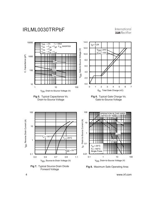
C, Capacitance (pF)I SD , Reverse Drain Current (A)V GS , Gate-to-Source Voltage (V)I D , Drain-to-Source Current (A)<strong>IRLML0030TRPbF</strong>100001000V GS = 0V, f = 1 MHZC iss= C gs+ C gd, C dsSHORTEDC rss= C gdC oss= C ds+ C gd14.012.010.0I D = 5.2AV DS = 24VV DS = 15V8.06.0100C oss4.0C rss2.010C iss0 1 2 3 4 5 6 71 10 100V DS , Drain-to-Source Voltage (V)0.0Q G ,Total Gate Charge (nC)Fig 5. Typical Capacitance Vs.Drain-to-Source VoltageFig 6. Typical Gate Charge Vs.Gate-to-Source Voltage100100OPERATION IN THIS AREALIMITED BY R DS (on)1010100µsec1T J = 150°CT J = 25°C0.10.3 0.5 0.7 0.9 1.1V SD , Source-to-Drain Voltage (V)Fig 7. Typical Source-Drain DiodeForward VoltageV GS = 0V10.1T A = 25°C10msec1msecTj = 150°CSingle Pulse0.010.1 1 10 100V DS , Drain-to-Source Voltage (V)Fig 8. Maximum Safe Operating Area4 www.irf.com