Tapered meander slot antenna for dual band personal wireless ...
Tapered meander slot antenna for dual band personal wireless ...
Tapered meander slot antenna for dual band personal wireless ...

You also want an ePaper? Increase the reach of your titles
YUMPU automatically turns print PDFs into web optimized ePapers that Google loves.
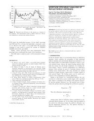
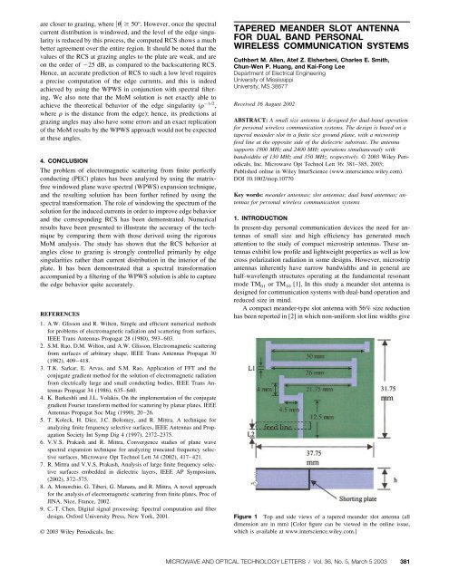
Figure 2 Top view of a tapered <strong>meander</strong> <strong>slot</strong> <strong>antenna</strong> with variable <strong>slot</strong>width [Color figure can be viewed in the online issue, which is available atwww.interscience.wiley.com.]Figure 4 Return loss <strong>for</strong> the tapered <strong>meander</strong> <strong>slot</strong> <strong>antenna</strong> design of Fig.1 [Color figure can be viewed in the online issue, which is available atwww.interscience.wiley.com.]rise to lower operating frequency of the <strong>antenna</strong>. In this paper weshow that a <strong>dual</strong>-frequency operation is achieved by using atapered <strong>meander</strong> <strong>slot</strong> <strong>antenna</strong> with a short-ended microstrip linefeed. The tapered <strong>meander</strong> <strong>slot</strong> <strong>antenna</strong> was derived from [3] inwhich a <strong>meander</strong> line was tapered to achieve operation at lowerfrequencies. The <strong>band</strong>s of interest <strong>for</strong> this research project arethose of <strong>wireless</strong> local area networks (WLANs), and <strong>personal</strong>communication systems (PCS).2. MEANDER SLOT ANTENNA DESIGNThe initial design of a tapered <strong>meander</strong> <strong>slot</strong> <strong>antenna</strong> is shown inFigure 1 where the <strong>slot</strong> width is 1.5 mm and L1 varies from 0 to0.75 mm. The <strong>antenna</strong> is constructed by making a <strong>meander</strong> <strong>slot</strong> ina perfectly conducting plane supported by a dielectric substrate of1.905 mm thickness and relative dielectric constant of 9.2. The<strong>antenna</strong> is excited by a microstrip feed line. The edge of the feedline is shorted to the perfectly conducting plane using a shortingwall. The width and length of the feed line can be adjusted toachieve a good input match. The improved design is shown inFigure 2 where the horizontal <strong>slot</strong>s of the <strong>meander</strong> are varied inwidth from 1.5 to 0.5 mm in order to support the 1800 MHz as wellas the 2400 MHz operating frequencies.3. SIMULATION AND RESULTSA. Confirmation of Simulated ResultsThe Advance Design System (ADS) software package of AgilentTechnologies [4] is used to analyze this type of <strong>antenna</strong>. Toconfirm the results produced by ADS, the finite difference timedomain (FDTD) method is used <strong>for</strong> the computation of the returnloss of a sample case. For the sake of simplicity and speed in theFDTD simulation a design with dimension divisible by 0.5 mm isused. For this reason an initial design similar to that of Figure 1 issimulated with the second horizontal <strong>slot</strong> at 22 mm long instead of21.75 mm and L1 equal to zero with a <strong>slot</strong> width of 1.5 mm. Thewidth of the excitation strip and L2 is equal to 2.5 mm and 2 mm,respectively.To achieve stability in the FDTD simulation of the <strong>antenna</strong>,parameters were chosen to give 30 cells per wavelength at thehighest usable frequency. The <strong>meander</strong> <strong>slot</strong> is oriented in the y-zplane with 40 cells between the <strong>antenna</strong> and the absorbing boundarygiving a total mesh dimension of 84 156 144 cells in thexˆ, ŷ, and ẑ directions, respectively. The special increments y andz were chosen to be 0.5 mm and x was chosen as 0.476 mm togive a dielectric substrate height of 4 x. The width of the <strong>slot</strong> is6 z, and the spacing between the <strong>meander</strong> turns is 8 z. TheFigure 3 Comparison of return loss computations based on ADS andFDTD simulations [Color figure can be viewed in the online issue, whichis available at www.interscience.wiley.com.]Figure 5 Input resistance <strong>for</strong> tapered <strong>meander</strong> <strong>slot</strong> <strong>antenna</strong> design of Fig.1 [Color figure can be viewed in the online issue, which is available atwww.interscience.wiley.com.]382 MICROWAVE AND OPTICAL TECHNOLOGY LETTERS / Vol. 36, No. 5, March 5 2003
Figure 6 Return loss <strong>for</strong> the tapered <strong>meander</strong> <strong>slot</strong> <strong>antenna</strong> design of Fig.1 [Color figure can be viewed in the online issue, which is available atwww.interscience.wiley.com.]Figure 8 Return loss comparison of initial and final designs operating at1800 MHz and 2400 MHz [Color figure can be viewed in the online issue,which is available at www.interscience.wiley.com.]width of the excitation strip is 5 z. The time step used in thesimulation is t 0.852 ps, the Gaussian half width is 25.017 ps, and the time delay t 0 is 4.5 [5]. A total number of 4000time steps were used in order to ensure that the time domainresponse approaches zero. The results are shown in Figure 3 whichshows the comparison of the return loss derived from the ADSsimulation and the FDTD method. Good agreement is observedwhich validates the design procedure using ADS.B. Simulated DesignAn initial design of Figure 1 is done with the width of theexcitation strip and L2 equal to 2.25 and 2 mm, respectively. Thereturn loss is shown in Figure 4. It can be seen that with an increasein L1 the operating frequency of the <strong>antenna</strong> is shifted down. Thedesign presented in Figure 1 yields a maximum <strong>band</strong>width ofabout 700 MHz when L1 is 0.75 mm and a minimum <strong>band</strong>widthof about 670 MHz with L1 equal to zero. It is found that theincrease of L1 leads to an increased variation of the input resistanceas shown in Figure 5.The return loss observed from the design of Figure 2 is shownin Figure 6. As the horizontal <strong>slot</strong> width (W1) is varied from 1.5to 0.5 mm the second resonance at 2420 MHz remains constantwhere as the first resonance is shifted down from about 2040 MHzto about 1803 MHz. The numerical results of Figure 7 indicate thatthe variations of the input resistance of this design increases withthe decrease of W1.In order to achieve a design working at both 1800 MHz and2400 MHz operating frequencies both designs of Figure 1 andFigure 2 were combined. With L1 equal to 0.25 mm and W1 equalto 0.5 mm, Figure 8 shows the return loss of the resulting designoperating at 1800 MHz and 2400 MHz. The input resistance isdepicted in Figure 9 and shows more variation within the operatingfrequencies compared to the initial case with no tuning.The radiation pattern <strong>for</strong> the final design is shown in Figures 10and 11 operating at 1800 and 2400 MHz, respectively. The <strong>band</strong>widthat the first resonance centered at 1800 MHz is 130 MHz witha directivity of about 3.62 dB. The operating <strong>band</strong>width of thesecond resonance at 2400 MHz is about 350 MHz with directivityof 4.22 dB. Extensive simulation results reveal that the radiationpattern remains constant over both operating <strong>band</strong>widths. For thesake of providing parametric study <strong>for</strong> <strong>antenna</strong> designers, furtheranalysis of the final design working at 1800 and 2400 MHz wasachieved. In what follows the effects of the spacing between turns,ds, and the taper angle are reported.Figure 12 shows the return loss due to changes in the spacingbetween turns annotated by S. It is shown that both operatingFigure 7 Input resistance <strong>for</strong> the tapered <strong>meander</strong> <strong>slot</strong> <strong>antenna</strong> design ofFig. 1 [Color figure can be viewed in the online issue, which is availableat www.interscience.wiley.com.]Figure 9 Input resistance comparison of initial and final designs operatingat 1800 MHz and 2400 MHz [Color figure can be viewed in theonline issue, which is available at www.interscience.wiley.com.]MICROWAVE AND OPTICAL TECHNOLOGY LETTERS / Vol. 36, No. 5, March 5 2003 383
Figure 10 Radiation pattern of the final design at 1800 MHz [Colorfigure can be viewed in the online issue, which is available at www.interscience.wiley.com.]Figure 11 Radiation pattern of final design at 2400 MHz [Color figurecan be viewed in the online issue, which is available at www.interscience.wiley.com.]frequencies are shifted up <strong>for</strong> an increase in S, with S equal to 4mm being the case of the final design. When ds is varied from 11to 15.5 mm small changes in the first operating frequency areobserved. However, from the return loss of Figure 13, the secondoperating frequency is clearly being shifted down as ds is increased.Figure 14 again demonstrates this behavior by showing avery slight increase of the operating frequency at the first resonanceand a more apparent decrease of the operating frequency atthe second resonance as ds is increased.Figure 15 shows the return loss <strong>for</strong> the initial design of Figure1 with L1 equal to zero as the taper angle is varied. As expected,increasing the taper angle causes a decrease in the operatingfrequencies of the <strong>antenna</strong> due to the overall length of the <strong>meander</strong><strong>slot</strong> being increased. With an increase in the taper angle a decreasein the <strong>band</strong>width of operation is observed. Variations in the dielectricsubstrate height and dielectric constant value were alsolooked at and the effects on the return loss as seen in Figures 16and 17 are found to be minimal. Figure 16 shows the operatingfrequencies shifting down <strong>for</strong> an increase in the substrate height. InFigure 17 the operating frequency is shifted down also <strong>for</strong> anincrease in the dielectric constant.Figure 12 Return loss <strong>for</strong> different S values [Color figure can be viewedin the online issue, which is available at www.interscience.wiley.com.]384 MICROWAVE AND OPTICAL TECHNOLOGY LETTERS / Vol. 36, No. 5, March 5 2003
Figure 13 Return loss <strong>for</strong> different ds values [Color figure can beviewed in the online issue, which is available at www.interscience.wiley.com.]Figure 16 Return loss <strong>for</strong> various heights of the dielectric substrate[Color figure can be viewed in the online issue, which is available atwww.interscience.wiley.com.]Figure 14 Changes in operating frequencies <strong>for</strong> different values of ds[Color figure can be viewed in the online issue, which is available atwww.interscience.wiley.com.]5. CONCLUSIONA new design of a tapered <strong>meander</strong> <strong>slot</strong> <strong>antenna</strong> is presented with<strong>dual</strong>-<strong>band</strong> operation at 1800 and 2400 MHz with 130 MHz and350 MHz <strong>band</strong>widths, respectively. The <strong>antenna</strong> dimensions areFigure 15 Return loss <strong>for</strong> various taper angles of the initial design withL1 0 [Color figure can be viewed in the online issue, which is availableat www.interscience.wiley.com.]Figure 17 Return loss <strong>for</strong> various values of the dielectric constant [Colorfigure can be viewed in the online issue, which is available at www.interscience.wiley.com.]small to fit in most currently used <strong>personal</strong> communication devices.This <strong>antenna</strong> shows no significant variations in radiationpattern characteristics over the <strong>band</strong>widths of both operating frequencies.The effect of geometrical and electrical parameters havebeen studied and reported to aid in the design process of this classof <strong>antenna</strong>s.REFERENCES1. K.-L. Wong, Compact and Broad<strong>band</strong> Microstrip Antennas, John Wileyand Sons, New York, NY, 2002.2. J.-M. Kim, J.-G. Yook, W.-Y. Song, Y.-J. Yoon, J.-Y. Park, and H.-K.Park, Compact <strong>meander</strong>-type <strong>slot</strong> <strong>antenna</strong>s, 2001 IEEE Antenna PropagatSymp Proceedings, TX, (2001), 724–726.3. C.-W.P. Huang, J.B. Chen, A.Z. Elsherbeni, and C.E. Smith, FDTDCharacterization of Meander Line Antennas <strong>for</strong> RF and Wireless Communications,Electromagnetic Wave Monograph Series, Progress inElectromagnetic Research (PIER 24), Chief Editor: J.A. Kong, 24(1999), 185–200.4. Agilent Technologies, Advance Design Systems 1.5 Momentum, ApendixA, December, 2000.5. Atef Z. Elsherbeni, Class Notes, Electrical Engineering Department,The University of Mississippi, January 2002.© 2003 Wiley Periodicals, Inc.MICROWAVE AND OPTICAL TECHNOLOGY LETTERS / Vol. 36, No. 5, March 5 2003 385