A wideband coplanar-waveguide-fed multi-slot antenna for radar ...
A wideband coplanar-waveguide-fed multi-slot antenna for radar ...
A wideband coplanar-waveguide-fed multi-slot antenna for radar ...

You also want an ePaper? Increase the reach of your titles
YUMPU automatically turns print PDFs into web optimized ePapers that Google loves.
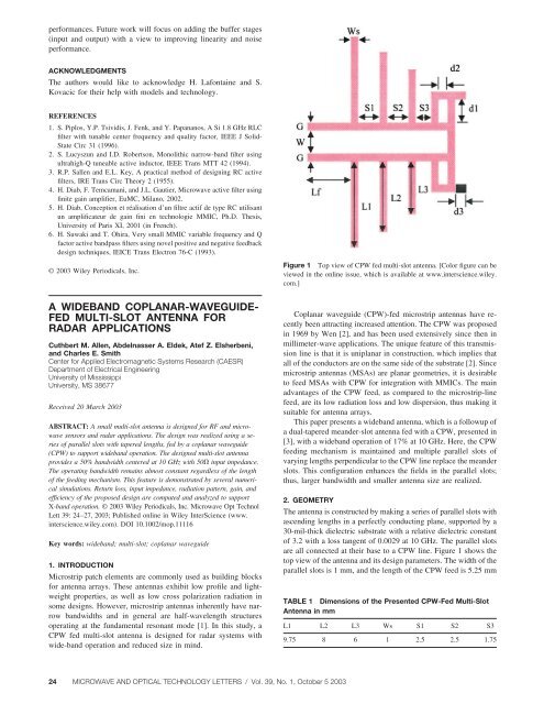
per<strong>for</strong>mances. Future work will focus on adding the buffer stages(input and output) with a view to improving linearity and noiseper<strong>for</strong>mance.ACKNOWLEDGMENTSThe authors would like to acknowledge H. Lafontaine and S.Kovacic <strong>for</strong> their help with models and technology.REFERENCES1. S. Piplos, Y.P. Tsividis, J. Fenk, and Y. Papananos, A Si 1.8 GHz RLCfilter with tunable center frequency and quality factor, IEEE J Solid-State Circ 31 (1996).2. S. Lucyszun and I.D. Robertson, Monolithic narrow-band filter usingultrahigh-Q tuneable active inductor, IEEE Trans MTT 42 (1994).3. R.P. Sallen and E.L. Key, A practical method of designing RC activefilters, IRE Trans Circ Theory 2 (1955).4. H. Diab, F. Temcamani, and J.L. Gautier, Microwave active filter usingfinite gain amplifier, EuMC, Milano, 2002.5. H. Diab, Conception et réalisation d’un filtre actif de type RC utilisantun amplificateur de gain fini en technologie MMIC, Ph.D. Thesis,University of Paris XI, 2001 (in French).6. H. Suwaki and T. Ohira, Very small MMIC variable frequency and Qfactor active bandpass filters using novel positive and negative feedbackdesign techniques, IEICE Trans Electron 76-C (1993).© 2003 Wiley Periodicals, Inc.A WIDEBAND COPLANAR-WAVEGUIDE-FED MULTI-SLOT ANTENNA FORRADAR APPLICATIONSCuthbert M. Allen, Abdelnasser A. Eldek, Atef Z. Elsherbeni,and Charles E. SmithCenter <strong>for</strong> Applied Electromagnetic Systems Research (CAESR)Department of Electrical EngineeringUniversity of MississippiUniversity, MS 38677Received 20 March 2003ABSTRACT: A small <strong>multi</strong>-<strong>slot</strong> <strong>antenna</strong> is designed <strong>for</strong> RF and microwavesensors and <strong>radar</strong> applications. The design was realized using a seriesof parallel <strong>slot</strong>s with tapered lengths, <strong>fed</strong> by a <strong>coplanar</strong> <strong>waveguide</strong>(CPW) to support <strong>wideband</strong> operation. The designed <strong>multi</strong>-<strong>slot</strong> <strong>antenna</strong>provides a 50% bandwidth centered at 10 GHz with 50 input impedance.The operating bandwidth remains almost constant regardless of the lengthof the feeding mechanism. This feature is demonstrated by several numericalsimulations. Return loss, input impedance, radiation pattern, gain, andefficiency of the proposed design are computed and analyzed to supportX-band operation. © 2003 Wiley Periodicals, Inc. Microwave Opt TechnolLett 39: 24–27, 2003; Published online in Wiley InterScience (www.interscience.wiley.com). DOI 10.1002/mop.11116Key words: <strong>wideband</strong>; <strong>multi</strong>-<strong>slot</strong>; <strong>coplanar</strong> <strong>waveguide</strong>1. INTRODUCTIONMicrostrip patch elements are commonly used as building blocks<strong>for</strong> <strong>antenna</strong> arrays. These <strong>antenna</strong>s exhibit low profile and lightweightproperties, as well as low cross polarization radiation insome designs. However, microstrip <strong>antenna</strong>s inherently have narrowbandwidths and in general are half-wavelength structuresoperating at the fundamental resonant mode [1]. In this study, aCPW <strong>fed</strong> <strong>multi</strong>-<strong>slot</strong> <strong>antenna</strong> is designed <strong>for</strong> <strong>radar</strong> systems withwide-band operation and reduced size in mind.Figure 1 Top view of CPW <strong>fed</strong> <strong>multi</strong>-<strong>slot</strong> <strong>antenna</strong>. [Color figure can beviewed in the online issue, which is available at www.interscience.wiley.com.]Coplanar <strong>waveguide</strong> (CPW)-<strong>fed</strong> microstrip <strong>antenna</strong>s have recentlybeen attracting increased attention. The CPW was proposedin 1969 by Wen [2], and has been used extensively since then inmillimeter-wave applications. The unique feature of this transmissionline is that it is uniplanar in construction, which implies thatall of the conductors are on the same side of the substrate [2]. Sincemicrostrip <strong>antenna</strong>s (MSAs) are planar geometries, it is desirableto feed MSAs with CPW <strong>for</strong> integration with MMICs. The mainadvantages of the CPW feed, as compared to the microstrip-linefeed, are its low radiation loss and low dispersion, thus making itsuitable <strong>for</strong> <strong>antenna</strong> arrays.This paper presents a <strong>wideband</strong> <strong>antenna</strong>, which is a followup ofa dual-tapered meander-<strong>slot</strong> <strong>antenna</strong> <strong>fed</strong> with a CPW, presented in[3], with a <strong>wideband</strong> operation of 17% at 10 GHz. Here, the CPWfeeding mechanism is maintained and <strong>multi</strong>ple parallel <strong>slot</strong>s ofvarying lengths perpendicular to the CPW line replace the meander<strong>slot</strong>s. This configuration enhances the fields in the parallel <strong>slot</strong>s;thus, larger bandwidth and smaller <strong>antenna</strong> size are realized.2. GEOMETRYThe <strong>antenna</strong> is constructed by making a series of parallel <strong>slot</strong>s withascending lengths in a perfectly conducting plane, supported by a30-mil-thick dielectric substrate with a relative dielectric constantof 3.2 with a loss tangent of 0.0029 at 10 GHz. The parallel <strong>slot</strong>sare all connected at their base to a CPW line. Figure 1 shows thetop view of the <strong>antenna</strong> and its design parameters. The width of theparallel <strong>slot</strong>s is 1 mm, and the length of the CPW feed is 5.25 mmTABLE 1 Dimensions of the Presented CPW-Fed Multi-SlotAntenna in mmL1 L2 L3 Ws S1 S2 S39.75 8 6 1 2.5 2.5 1.7524 MICROWAVE AND OPTICAL TECHNOLOGY LETTERS / Vol. 39, No. 1, October 5 2003
Figure 2 Return loss <strong>for</strong> different values of d1. [Color figure can beviewed in the online issue, which is available at www.interscience.wiley.com.]with width W and gap G equal to 2.5 and 1 mm, respectively. Theother dimensions are given in Table 1.3. SIMULATION AND RESULTSThe related simulation and analysis are per<strong>for</strong>med using AgilentTechnologies’ commercial computer software package, AdvancedDesign System (ADS), which is based on the method of moments(MoM) technique <strong>for</strong> layered media. The ADS simulator, calledMomentum, solves mixed potential integral equations (MPIE)using full-wave Green’s functions [4]. The design shown in Figure1 was originally analyzed with d3 held constant at zero (that is,there is no extended tuning <strong>slot</strong>). With d3 held at zero and d2 heldat 1.5 mm, d1 was varied; the resultant return loss is shown inFigure 2. The return loss in Figure 2 shows that decreasing d1increases the resonant frequency, while it does not affect thebandwidth.Figure 3 shows the return loss when d3 and d1 are held at 0 and2.5 mm, respectively. These results show that the resonant frequencyand the bandwidth of the <strong>antenna</strong> are increased when d2 isdecreased. However, the return loss at the center frequenciesincreases as d2 is decreased.Next, while varying d3, d1 and d2 were held constant at 2.5 and1 mm, respectively. Increasing the tuning <strong>slot</strong> extension (d3)Figure 4 Return loss <strong>for</strong> different values of d3. [Color figure can beviewed in the online issue, which is available at www.interscience.wiley.com.]increased the return loss at the resonant frequency. The relatedresults are shown in Figure 4. However, extending d3 slightlyincreases the bandwidth and reduces the variation of the inputresistance across the bandwidth of operation of the <strong>antenna</strong>, asshown in Figure 5.Another way in which the operating bandwidth of the <strong>antenna</strong>could be adjusted is by controlling the length Lf (the length of theCPW feed line). Figures 6 and 7 show the return loss and inputresistance <strong>for</strong> different lengths of Lf, respectively. Clearly when Lfis reduced the bandwidth of the <strong>antenna</strong> shifts up with an increasein bandwidth. However, when Lf is increased the bandwidth shiftsdown with a decrease in total bandwidth. From Figure 6 a bandwidthof 50% centered at 10 GHz is achieved <strong>for</strong> Lf equal to 4 mm.The results in Figure 7 show that the input resistance exhibits lessvariation within the bandwidth of operation when Lf is increased.There<strong>for</strong>e, the shortest possible length of CPW feed should beused.Since any changes in the CPW feed line length affects theper<strong>for</strong>mance of the <strong>antenna</strong>, a method needs to be developed tofeed the <strong>antenna</strong> from sources with varying distances from the<strong>antenna</strong> feed point. This is necessary because it may not bepractical to feed the <strong>antenna</strong> at exactly that point. To accomplishthis, a 50 CPW transmission line is designed along with aFigure 3 Return loss <strong>for</strong> different values of d2. [Color figure can beviewed in the online issue, which is available at www.interscience.wiley.com.]Figure 5 Input resistance <strong>for</strong> different values of d3. [Color figure can beviewed in the online issue, which is available at www.interscience.wiley.com.]MICROWAVE AND OPTICAL TECHNOLOGY LETTERS / Vol. 39, No. 1, October 5 2003 25
Figure 6 Return loss <strong>for</strong> different values of Lf. [Color figure can beviewed in the online issue, which is available at www.interscience.wiley.com.]Figure 9 Return loss <strong>for</strong> different values of Lc. [Color figure can beviewed in the online issue, which is available at www.interscience.wiley.com.]Figure 7 Input resistance <strong>for</strong> different values of Lf. [Color figure can beviewed in the online issue, which is available at www.interscience.wiley.com.]Figure 10 Return loss <strong>for</strong> ADS and FDTD. [Color figure can be viewedin the online issue, which is available at www.interscience.wiley.com.]transition line to connect the <strong>antenna</strong> to the 50 CPW line. Thedesign of the 50 CPW transmission line yields values <strong>for</strong> W andG as 5.718 and 0.25 mm, respectively. The length of the transitionline from the 50 CPW line to the <strong>antenna</strong> is 0.27 mm. Figure 8shows the arrangement used with this <strong>antenna</strong>. Figure 9 presentsthe return loss of the <strong>antenna</strong> with the source now applied to the50 CPW transmission line. For different lengths of the 50 CPWline, the bandwidth of the <strong>antenna</strong> remains almost constant. TheFigure 8 Transition between 50 CPW transmission line and CPW <strong>fed</strong><strong>multi</strong>-<strong>slot</strong> <strong>antenna</strong>. [Color figure can be viewed in the online issue, whichis available at www.interscience.wiley.com.]Figure 11 Input impedance <strong>for</strong> ADS and FDTD. [Color figure can beviewed in the online issue, which is available at www.interscience.wiley.com.]26 MICROWAVE AND OPTICAL TECHNOLOGY LETTERS / Vol. 39, No. 1, October 5 2003
Figure 12 Radiation pattern at 10 GHz: (a) z-y plane, (b) z-x plane, (c) x-y palne, (d) toal 3D pattern. [Color figure can be viewed in the online issue, whichis available at www.interscience.wiley.com.]results shown in Figure 9 are <strong>for</strong> the <strong>antenna</strong> design with Lf set at4 mm. Note that the bandwidth of operation does not change asmuch as it did in Figure 6, and the resonant frequency does notshift.To confirm the results produced by ADS Momentum, thefinite-difference time-domain (FDTD) method is used. The returnloss <strong>for</strong> the <strong>antenna</strong> design with Lf set at 4 mm operating over theentire X-band range of frequencies is reproduced along with theinput resistance. To achieve stability in the FDTD simulation ofthe <strong>antenna</strong>, parameters were chosen to support 30 cells per wavelengthat the highest usable frequency. The <strong>multi</strong>-<strong>slot</strong> <strong>antenna</strong> isoriented in the x–y plane with 30 cells between the feeding edgeof <strong>antenna</strong> and the related absorbing boundary. The other threeedges are extended to the absorbing boundary in order to simulatean infinite ground plane similar to the design analysis used in ADS.The total mesh dimensions are 135 155 63 cells in the x, y,and z directions, respectively. The spatial increments x and yare chosen to be 0.25 mm and z is chosen to be 0.254 mm.There<strong>for</strong>e, the dielectric substrate is 3 z to give a total of 30 mil,and the width of the <strong>slot</strong>s is 4 y. The time step used in thesimulation is 0.43559 ps, the Gaussian wave<strong>for</strong>m half width is 12.709 ps, and the time delay t o is 4.5 [5]. A total number of 5000time steps is used in order to ensure that the time domain responseapproaches zero. The results are shown in Figures 10 and 11,which show the return loss and input resistance derived from theADS and the FDTD simulations, respectively, <strong>for</strong> comparison.Good agreement, which validates the design procedure using ADSMomentum, is observed.The radiation pattern of the <strong>multi</strong>-<strong>slot</strong> <strong>antenna</strong> designed with Lfequal to 4 mm is shown in Figure 12 at an operating frequency of10 GHz. The <strong>antenna</strong> design has a directivity of 4.829 dB, a gainof 4.385 dB, and an efficiency of 90.8%.<strong>multi</strong>-<strong>slot</strong> <strong>antenna</strong> provided high efficiency of about 90% anddirectivity of 4.829 dB. This <strong>antenna</strong> shows no significant variationsin radiation pattern characteristics over the bandwidth ofoperation. The effect of geometrical and electrical parameters werestudied and reported to aid in the design process of this new classof <strong>antenna</strong>s.REFERENCES1. K-L Wong, Compact and broadband microstrip <strong>antenna</strong>s, Wiley, NewYork, 2002.2. R.N. Simons, Coplanar <strong>waveguide</strong> circuits, components, and systems,Wiley, New York, 2001, pp. 1–6, 422–424.3. C.M. Allen, A.Z. Elsherbeni, and C.E. Smith, 2002 USNC/URSI NationalRadio Science Meeting, San Antonio, TX, 2002, p. 363.4. Agilent Technologies, Advance Design Systems 1.5 Momentum, AppendixA, 2000.5. A.Z. Elsherbeni, C.G. Christodoulou, and J. Gomez-Tagle, The finitedifference time domain technique <strong>for</strong> microstrip <strong>antenna</strong>s, in Handbookof <strong>antenna</strong>s in wireless communications, L. Godara (Ed.), CRC Press,Boca Raton, FL, 2001.© 2003 Wiley Periodicals, Inc.4. CONCLUSIONA new design of a CPW <strong>fed</strong> <strong>multi</strong>-<strong>slot</strong> <strong>antenna</strong> has been presented,operating with a bandwidth of about 50%, centered at 10 GHz. TheMICROWAVE AND OPTICAL TECHNOLOGY LETTERS / Vol. 39, No. 1, October 5 2003 27