- Page 1 and 2: 9914V TAPE UNITSERVICING MANUALDocu
- Page 3 and 4: Bescheinigung des HerstellersHiermi
- Page 5 and 6: INTERNAL CODE LICENSEPLEASE READ TH
- Page 7 and 8: Table of ContentsSection 1 9914V Ov
- Page 9 and 10: Section 3 Fault-Finding and Calibra
- Page 11 and 12: 7.2 MaIns Transformer and Switch ..
- Page 13 and 14: 7.17 Pertec Cache Interface Board .
- Page 15 and 16: Illustrations of Parts8.2.1 TAPE PA
- Page 17 and 18: 1.9914V OverviewThis 9914V Servicin
- Page 19 and 20: 1.2.3 Access, Modularity, and Tools
- Page 22 and 23: 1.3 Short-Form SpecificationTape Ty
- Page 24 and 25: 1.4 StreamingTo maintain streaming,
- Page 26 and 27: 1.5 lor. Mains SystemsD€finition:
- Page 28 and 29: c) Miscellaneous circuits:i) to acc
- Page 30 and 31: !IOperator"s PanelI~Mlcroprocessor~
- Page 32 and 33: ) Drive CurrentsThe processor outpu
- Page 34 and 35: ) LocatingIn order to check the loc
- Page 36 and 37: 2.3 Data Control Board Description2
- Page 39: Signal MODEa MODE1 MODE2 MODE3Meani
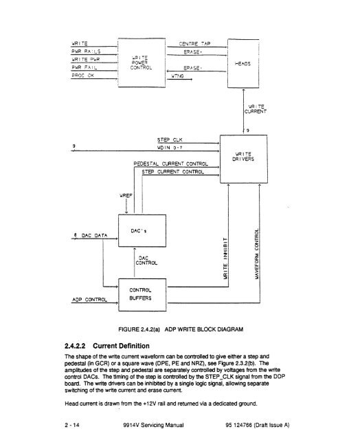
- Page 43 and 44: Under fixed gain conditions, the am
- Page 45 and 46: tilE THRESI-'OLD .. . t ...........
- Page 47 and 48: 2.5.3.1 Control StrategyThere are f
- Page 49 and 50: 2.6 Pre-Amplifier DescriptionThis s
- Page 51 and 52: SKI I! SK2CJ '---..;;.......,;----'
- Page 53 and 54: 2.8.3 SCSI InterfaceThe SCSI Contro
- Page 55 and 56: 3.Fault Finding3.1 Scope of Section
- Page 57 and 58: Hub Sensor pcb-PLHS,ITachoI~PlAL II
- Page 59 and 60: DisplayExplanationSuspect FRU* BOT
- Page 61 and 62: Display Explanation Suspect FRUOKTh
- Page 63 and 64: 95 125456 (Draft Issue D) Fault Fin
- Page 65 and 66: 3.3.4 On-line IndicationsThe full l
- Page 67 and 68: 3.4 Fault-Finding Routines3.4.1 Int
- Page 69 and 70: 0lFaultl Possible causesI nvestigat
- Page 71 and 72: Faultl Possible causes Investigatio
- Page 73 and 74: o11Fault I Possible causes Investig
- Page 76 and 77: I\.)I\.)Fault I Possible causesInve
- Page 78 and 79: 3.6 Manual Tape ThreadingSince the
- Page 80 and 81: Re-calibration of the 98 i Li.\t ;;
- Page 82 and 83: Configuration bytes 06 onwards are
- Page 84 and 85: 4.3 Configuration Byte 07 - Host In
- Page 86 and 87: 4.5 Configuration Byte 09 - Host In
- Page 88 and 89: 4.7 Configuration Byte 11 - Conditi
- Page 90 and 91:
4.9 - Configuration Byte 13 - Misce
- Page 92 and 93:
4.11 Configuration BytE.; '~g - Mis
- Page 94 and 95:
Option0102030405MeaningDNSDIS-1DNSD
- Page 96 and 97:
This page has no technical content4
- Page 98 and 99:
5.1.2 ',-ite CurrentFallaw the flow
- Page 100 and 101:
No. Function No. Function00 NULL PR
- Page 102 and 103:
Program 03NoteDescriptionILWD Line
- Page 104 and 105:
When run on-line, the programs expe
- Page 106 and 107:
Program 14DescriptionSet Block Leng
- Page 108 and 109:
Pro-:;r~UI 25Write, Backspace, Read
- Page 110 and 111:
Program 32 ~~;ce " ~IocksNotes - ;"
- Page 112 and 113:
i t 1 7 6 5 4 3 1 2 1 0I I I 1 I 1
- Page 114 and 115:
L should not be displayed with the
- Page 116 and 117:
EXIT Denotes the first exit point o
- Page 118 and 119:
Program 65Program 66DescriptionErro
- Page 120 and 121:
Prog"ram 69DescriptionError CodesIn
- Page 122 and 123:
Error Codes~: : AL f',l;:·)le cali
- Page 124 and 125:
Program 80Set Default NVR ValuesNot
- Page 126 and 127:
Program 98DescriptionError CodesCle
- Page 128 and 129:
6.4 Status Byte F4When an on-line d
- Page 130 and 131:
6.7 Status Byte F7Status byte F7 co
- Page 132 and 133:
· - -6.9 Status Byte F9Status byte
- Page 134 and 135:
6.11 Status By'"_-; ~ i ~Status byt
- Page 136 and 137:
6.16 Status Byte F16Bit Name Meanin
- Page 138 and 139:
it 7 bit 6bit 5 bit 4 bit 3 bit 2 b
- Page 140 and 141:
6.18 Condensed Status BytesThe 9914
- Page 142 and 143:
.....(J)ClWRITE ERR LOGbit 7 bit 62
- Page 144 and 145:
7.1.3 Electrical Servicing Equipmen
- Page 146 and 147:
7.2 Mains Tra.~- ad SWitchThe mains
- Page 148 and 149:
7.2.4.1 Wiring the AC Supply PlugWa
- Page 150 and 151:
7.4.4 SettingThe Servo Control perf
- Page 152 and 153:
Notes to Table 7.5.3:i) dual-functi
- Page 154 and 155:
ALLEN KEYE~ECTORSUTTONTOGGLEARf\iv)
- Page 156 and 157:
7.8 Tape Path Assembly7.8.1 Functio
- Page 158 and 159:
7.9.2 LocationThe tape cleaner is m
- Page 160 and 161:
7.11 rension Arm Assembly7.11.1 Fun
- Page 162 and 163:
The 9914V Data Central boards use E
- Page 164 and 165:
vi) Disconnect the IDC connectors t
- Page 166 and 167:
No attempt should be made to discon
- Page 168 and 169:
7.17.2 LocationThe PCI board is a p
- Page 170 and 171:
8.1 Available Spares8.1.1 Major Spa
- Page 172 and 173:
8.1.3 Subsidiary Spares Lisi:Parts
- Page 174 and 175:
\\-FIGURE 8.2.1TAPE PATH ASSEMBLY8-
- Page 176 and 177:
FIGURE 8.2.2 PARTS ABOVE THE TAPE P
- Page 178 and 179:
FIGURE 8.2.3(a) PARTS BELOW THE TAP
- Page 180 and 181:
FIGURE 8.2.3(b) PARTS BELOW THE TAP
- Page 182 and 183:
02 _____lG(3FIGURE 8.2.4 SUPPLY HUB
- Page 184 and 185:
\2II\0FIGURE 8.2.5 COOLING FAN ASSE
- Page 186 and 187:
00I~00
- Page 188 and 189:
--1LU---a--- 01FIGURE 8.2.7 ANALOGU
- Page 190 and 191:
FIGURE 8.2.8 DIGITAL DATA PATHS BOA
- Page 192 and 193:
FIGURE 8.2.9 DATA CONTROL BOARD8 -
- Page 194 and 195:
00If\.)0>
- Page 196 and 197:
l-ClI I",-...1\I,II1\O~\III\----FIG
- Page 198 and 199:
loll 'eOIl~~10-I
- Page 200 and 201:
FIGURE 8.2.13 OPERATOR PANEL AND SW
- Page 202 and 203:
o17--ljII 1011----~.....FIGURE 8.2.
- Page 204 and 205:
FIGURE 8.2.15 MAINS SWITCH8 - 36 99
- Page 206 and 207:
-----.\2~\\ ~1~IOFIGURE 8.3.1SCSI B
- Page 208 and 209:
16 ________15 Y! ! II I' I1 I' ,0\
- Page 210 and 211:
\0{1b'5 13 16FIGURE 8.3.3 DC POWER
- Page 212 and 213:
~-------~IFIGURE 8.4.1MAINS TRANSFO
- Page 214 and 215:
FIGURE 8.4.2 HUB SENSOR PCB8 - 46 9
- Page 216 and 217:
12II10-lWI--fl---OIFIGURE 8.4.3 AIR
- Page 218 and 219:
D14DFIGURE 8.4.4 AC FUSE KIT8 - 50
- Page 220 and 221:
o\ft~o·~)bJa:1FIGURE 8.4.5 DC FUSE
- Page 222 and 223:
8 - 54MOTHERBOARDFIGURE 8.4.6 95 12
- Page 224:
This page has no 'technical content