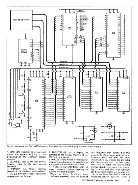
Circuit diagram of the full DATUM system, less the keyboard and display section shown in Fig. 6.1. RESET (RS). Initialises all devices andcauses the system to jump to thebeginning of the Monitor controlprogram.2. ESCAPE (E). Lets us exit one controlfunction ready for the next controlsequence.3. MEMORY (M). Allows memorycontents to be displayed and modified.4. GO (G). Provides a "start' instructionso programs can be run.5. REGISTERS (5). Lets us display thecontents of the internal registers of the6802 microprocessor.6. SINGLE STEP (R). Assists in "debugging"programs by allowing us to step througha program one instruction at a time.7. INCREMENT/DECREMENT. Lets usinspect memory contents, stepping theaddress in either direction.While all these functions wereconsidered essential, some will be usedless frequently than others. It is thuspossible to share some switches, withfunctions which are used less oftenrequiring two key presses, the first beingthe "second function" (2F) key. Otherkeys such as Reset and Escape mustoperate directly and cannot be shared.Fig. 3 shows how the seven functionscan be accommodated on six switches.So far we have described a minimummicroprocessor system, with aELECTRONICS Australia, November, 1982 89
DATUM microcomputerHOW IT WORKShexadecimal keypad for input, LEDdisplays for output, a processor andmemory. Two additional features havebeen included on the DATUM board.First, since the system is to be selfcontaineda simple logic probe has beenincluded on the board so that signals canbe monitored. Secondly, provision hasbeen made to expand DATUM whenrequired.<strong>The</strong> 44-pin edge connector, visible inphotographs of the board, brings out thedata, address and control lines forconnection to other equipment. Inaddition there is space on the board fora second PIA (Peripheral InterfaceAdapter) which provides 20 parallelInput/Output lines and an ACIA,providing a serial interface. With theaddition of 12V level translators this chipprovides an RS-232C channel forconnection to terminals and printers.With these additions DATUM canbecome more than a learning aid,finding a host of control andcommunications functions in realapplications.Fig. 2 summarises the design decisionstaken so far and presents a blockdiagram of the minimum DATUMsystem.How it worksLike most microprocessors theMC6802 is "bus" oriented. A commonparallel signal path consisting of data,address and control lines connects themain components of the system. Againin the interests of simplicity, not all thecontrol lines of the MC6802 are used inthe DATUM design.<strong>The</strong> RAM Enable (RE) line is tied to +5Vto enable the 128 bytes of on-chipmemory. <strong>The</strong> Memory Ready (MR) line isalso tied high. Its normal function is toallow the processor to wait for slowmemory devices which are not used inDATUM. "Standby" applies power to thefirst 32 bytes of the internal memory sothat in the event of a power failure thismemory can be powered <strong>from</strong> anemergency supply.HALT is not used, as we don't want tostop the processor at any time so thisline is also tied to +5V. Since HALT is notused, the Bus Available (BA) line whichindicates that the processor has halted isnot used and can be left open. <strong>The</strong>remaining control lines are used asfollows:RESET resets the MC6802. A pull-upresistor holds this line high until theReset pushbutton is operated. NMI, theNon-Maskable Interrupt, is also pulledhigh and connected to a pushbutton, inthis case the "Escape" function. IRQ is theinterrupt request line, allowingprocessing to be suspended and theRS c RESETE : ESCAPE2f ::SECOND FUNCTIONAMR 'AMORY AND REGISTER DISPLAYGiS : GO (START) AND SINGLE ST.UV : INCREMENT OR DECREMENTFlo. 3Fig. 3: Alternate key functionsare activated by pressingthe 2F key then the functionkey required.Fig. 4: Data, address andcontrol lines of the MC6802microprocessor used by theDATUM system.+5VESCAPERESETFig. 4processor directed to perform anotherprogram.VMA indicates that a "Valid memoryaddress" is available on the address bus,while the R/W line indicates whether amemory operation is a read or a writecommand. <strong>The</strong> Enable (E) line is theclock signal for the DATUM system. Thisclock signal is ANDed with VMA andused to initialise all the units on the bus.<strong>The</strong> frequency of E is a quarter of thecrystal clock frequency, so the 4MHzcrystal of DATUM provides a systemclock of 1MHz.Fig. 4 summarises the outputs of theMC6802 microprocessor and the linesused in the DATUM bus system. Pull upresistors have been added to the RESETand NMI lines since these must be heldhigh for the processor to operatecorrectly.Address decodingAs previously mentioned, not alladdress lines are decoded by theDATUM circuit. Address line 15 isignored while A14, A13 and Al2 aredecoded by a 74LS138 1-of-8 decoder toselect individual 4K blocks of memory.<strong>The</strong> remaining 12 address lines (<strong>from</strong> AOto All) provide a 4K (4096 bytes)addressing capacity. Memory in DATUMis thus divided into eight blocks, each of4K, for a total addressing capacity of 32Kbytes.I he next question is how to allocatethe available memory locations. Threeconstraints are set by the internalorganisation of the MC6802 chip:1. <strong>The</strong> internal 128 bytes of RAM mustbe the first 128 memory locations.2. After a Reset the last processor readsthe last two locations in memory (FFFEand FFFF hex) to find the address of the•CCr+ 5V 6802AST4MHzXIfEVMAIRORrwAOA14DOADDRESS LINESDATA LINESprogram to be run.3. After an Interrupt Request (IRQ) theprocessor reads address locations FFF8and FFF9 hex to determine the addressof the program to jump to.<strong>The</strong>se last two constraints suggest thatthe Monitor EPROM should be placed atthe top of the "memory map" topermanently store Reset and IRQpointers at the correct locations. <strong>The</strong>PIA, ACIA and RAM locations are thenallocated in a convenient order as shownin Fig. 5. Note that the PIA and ACIAeach occupy an entire 4K block ofmemory, even though each PIA has onlyfour registers which can be accessed,and the ACIA has only two.Because of the limited addressdecoding, each of these registers will berepeated in the memory map 1024times, but this is not important as long aswe are consistent in our programs. Sincethe amount of memory (RAM or ROM)on the DATUM board is less than 4K, thesame memory locations are alsorepeated throughout the memory map.For example the 2K EPROM is addressed7soan-iES,„INFERIORITY.,,COMPLEX.90 ELECTRONICS Australia, November, 1982