from GAMMATRON "DATUM" - The MESSUI Place
from GAMMATRON "DATUM" - The MESSUI Place
from GAMMATRON "DATUM" - The MESSUI Place

You also want an ePaper? Increase the reach of your titles
YUMPU automatically turns print PDFs into web optimized ePapers that Google loves.
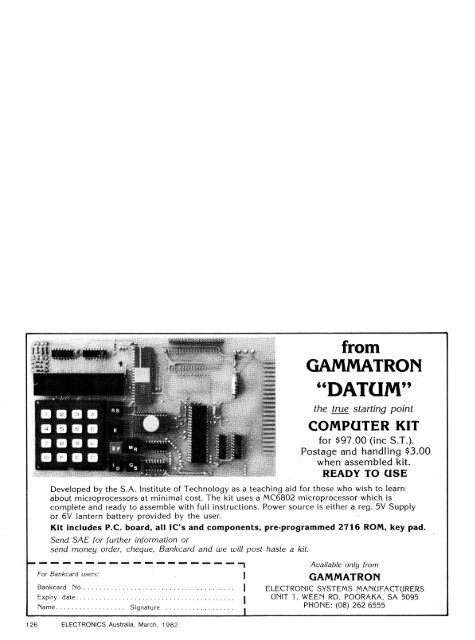
' . • • • • .... •*WO<strong>from</strong><strong>GAMMATRON</strong>"DATUM"the true starting pointCOMPUTER KITfor $97.00 (inc S.T.).Postage and handling $3.00when assembled kit.READY TO USEDeveloped by the S.A. Institute of Technology as a teaching aid for those who wish to learnabout microprocessors at minimal cost. <strong>The</strong> kit uses a MC6802 microprocessor which iscomplete and ready to assemble with full instructions. Power source is either a reg. 5V Supplyor 6V lantern battery provided by the user.Kit includes P.C. board, all IC's and components, pre-programmed 2716 ROM, key pad.Send SAE for further information orsend money order, cheque, Bankcard and we will post haste a kit.------------ ONE. MINIMFor Bankcard users:Bankcard No.Expiry dateNameSignatureAvailable only <strong>from</strong><strong>GAMMATRON</strong>ELECTRONIC SYSTEMS MANUFACTURERSUNIT 1, WEEN RD, POORAKA, SA 5095PHONE: (08) 262 6555126 ELECTRONICS Australia, March, 1982
a®Nring nnffRige, veM mrw©Gpap@@wo-13%DATUM: new low-costmicroprocessor trainerDo you want to learn about microprocessors <strong>from</strong> the ground up? Have you beenfollowing our series on "How to Program in Machine Language" but have nosystem to test out the concepts you've learnt? Or do you know a bit and arelooking for a low-cost dedicated microprocessor system for experiments or for usein a control application? If your answer to any of these questions is "yes" then thisis the project for you. Designed initially for teaching microprocessor concepts tostudents of Electronic Engineering, DATUM is a complete self-containedmicroprocessor system with everything needed to get you started.This project got its start when staff atthe School of Electronic Engineering atthe South Australian Institute ofTechnology noticed that students withtheir own microprocessor system athome performed much better thanthose who had to rely on the limitednumber of evaluation kits used in thelaboratories.It was obvious that to give every studentthe same opportunity a low costmicroprocessor trainer was required, sothe staff set to work. <strong>The</strong> result wasDATUM (Digital Aid for Teaching yoUMicroprocessors), an inexpensive, easyto use microprocessor kit based on theMotorola MC6802 processor.<strong>The</strong> design and development ofDATUM was a co-operative effort, withmany of the staff of the School of Elec-tronic Engineering contributing, and aSouth Australian company, Gammatron,undertaking the production of theprinted circuit board and kits for the project.Software for the Monitor programwas written by Mr P. D. O'Neill of theInstitute.One of the most important design decisionsfor the DATUM project was that ithad to be a completely self-containedsystem. A simple keypad on the boardprovides the means of inputting instructionsand data, while output is displayedon seven segment LED displays.Those readers who have followed ourseries on "Machine Language Programmingfor the 6800" will be in their elementhere, for the only way to programDATUM is by machine lanaguage andthe "instruction set" of the 6802 is iden-tical to that of the 6800. Both processorsare relatively simple but very versatile,and quite powerful enough for many advancedapplications.<strong>The</strong>re are only two differences betweenthe 6800 and 6802 processors. <strong>The</strong>6802 has an on-chip dock generator,needing only an external crystal. Moreimportantly, the MC6802 has 128 bytesof Random Access Memory on the chip,32 bytes of which can be placed in a lowpower "stand-by" mode to preserve importantdata when the rest of the systemis off. This is one reason why we chosethe 6802 for use in our Car Computerproject.In fact the Car Computer is a good illustrationof what is possible with a smallsystem such as this. Besides its use as alearning aid, DATUM can be put to useVSS 1HALT 2MR 3IRO 45NMI 6BA 7■1VCC aAO 9Al 10A211A3 12 dA413AS 14A6 15A7 16 VJA8 17A9 laA10 19A11 20bbfh40 RESET39 EXTAL38 XTAL37 E36 RE35 VCC STANDBY34 RIW33 DO32 Di31 D230 D329 D428 D527 D626 D725 Al524 A1423 A13222 As1s2 v21DATUM is a low-cost trainer for learning about microprocessors.Fig 1Fig. 1: Pin-outs of the MC6802.86 ELECTRONICS Australia, November, 1982
f ig.CRYSTAL7•SEGMENT DISPLAYKEY PAODATAMICROPROCESSOMC8802CONTROL LINESADDRESS LINES(15 ONLY)DATA LINES (BPIA 2SECONDPERIPHERALINTERFACEADAPTERBlock diagram of the fully expanded DATUM system.as a controller around the home (or thefactory), or expanded into a larger computersystem. Bus signals are brought outto a 44-way edge connector on one endof the board for this purpose and there isprovision on the board for additional Input/Output,with a PIA for parallel I/Oand an ACIA (Asynchronous CommunicationsInterface Adapter) for serialcommunication. -<strong>The</strong> double-sided DATUM printed circuitboard measures 228mm x 127mmand is silk-screened with componentlocations (although not componentvalues). <strong>The</strong> manual we received had thecomponent values hand-written after theparts list, although it is hoped that thiswill be corrected in final versions.<strong>The</strong> design of a minimummicroprocessor system<strong>The</strong> heart (or is that the brain?) of anymicroprocessor system is of course theprocessor chip itself. Pin connections forthe MC6802 are shown in Fig. 1. <strong>The</strong>processor has 16 address lines, and isPIA 1PERIPHERALINTERFACEADAPTER741S00141K OFRANDOMACCESSMEMORYLOGIC TESTERASYNCHRONOUSCOMUNICATIONSINTERFACEADAPTERLED44-PIN SOCKET+ 5V2K OFREAD ONLYMEMORY(MONITOR,thus capable of addressing 2 76 or 65,536separate memory locations.64K of memory is far more than weneed, so the first decision made in thedesign of DATUM was to decode blocksof memory, rather than individuallocations. This simplifies the circuitryrequired and reduces costs, at anegligible penalty — maximum memoryexpansion. This is 12K bytes in 4Kincrements.A minimal system will require bothRead Only Memory for permanentstorage of an operating program, andRAM (Random Access Memory) for userprograms. Static RAM is used since itavoids the complications of refreshingdynamic RAM (see our articles on theSuper-80 for details of a dynamic RAMsystem).Because we will be entering programsby hand it is unlikely that they willexceed about a hundred instructions.Around 2(X) bytes of RAM would besufficient, but the most readily availableand cost effective memory for ourpurposes is the 2114 static RAM chip.This chip is organised as 1K locations,each of four bits, so just two packageswill give us 1024 8-bit memory locations.<strong>The</strong> ROM package of DATUM holdsthe Monitor program — a collection ofroutines which assist the user incommunicating with the microprocessorsystem. Software is provided whichscans the keypad, drives the LED displaysand accepts input <strong>from</strong> the user.Depending on this input other routinesare activated which allow the contentsof memory to be inspected andchanged, the internal registers of the6802 to be displayed and the user'sprograms carried out.<strong>The</strong> Monitor program of DATUM is 1Kbytes long, and a complete listing of thesource code is included in with theinstruction manual supplied with the kit.Since the 2716 EPROM is a 2K deviceother programs which the user wishes tostore permanently can be programmedinto the unoccupied addresses. AnEPROM programmer suitable for thispurpose was described in our January1982 issue.Since DATUM is programmed inassembly language, hexadecimal outputwas decided on. Each 16-bit addresslocation and 8-bit data byte areconsidered as combinations of four bits,with each combination represented byone of 16 hexadecimal characters, thenumbers <strong>from</strong> 0 to 9 and letters <strong>from</strong> Ato F. A complete description of thehexadecimal numbering system is givenin Part One of "How to Program inMachine Language Language", EA March,1982.In hexadecimal, 16-bits are consideredas four groups of four, and 8-bit dataconsists of two groups of four. Sixdisplays are therefore required, four todisplay the address and two to displaythe data stored at that address.(11=1111111.■14,1HARDWARE SPECIFICATIONSProcessor: Motorola MC6802.Clock: /MHz.RAM: 1K x 8 on board, expandable to 12K externally, plus 128 bytes on chip.ROM: 2K (Monitor program occupies 1K).Display: Seven segment LED readouts (6).input: Hexadecimal keypad and six function select buttons.Output: Two PIA lines, optional extra PIA, ACIAPower requirements: Regulated +5V or 6V battery at 400mA.Programming: Hexadecimal machine code.UJA commercially available keypadprovides hexadecimal inputs while sixindividual pushbuttons are used forcontrol functions. Six switches providethe best balance between flexibility andcost. Key functions provided are:ELECTRONICS Australia, November, 1982 87
Circuit diagram of the full DATUM system, less the keyboard and display section shown in Fig. 6.1. RESET (RS). Initialises all devices andcauses the system to jump to thebeginning of the Monitor controlprogram.2. ESCAPE (E). Lets us exit one controlfunction ready for the next controlsequence.3. MEMORY (M). Allows memorycontents to be displayed and modified.4. GO (G). Provides a "start' instructionso programs can be run.5. REGISTERS (5). Lets us display thecontents of the internal registers of the6802 microprocessor.6. SINGLE STEP (R). Assists in "debugging"programs by allowing us to step througha program one instruction at a time.7. INCREMENT/DECREMENT. Lets usinspect memory contents, stepping theaddress in either direction.While all these functions wereconsidered essential, some will be usedless frequently than others. It is thuspossible to share some switches, withfunctions which are used less oftenrequiring two key presses, the first beingthe "second function" (2F) key. Otherkeys such as Reset and Escape mustoperate directly and cannot be shared.Fig. 3 shows how the seven functionscan be accommodated on six switches.So far we have described a minimummicroprocessor system, with aELECTRONICS Australia, November, 1982 89
DATUM microcomputerHOW IT WORKShexadecimal keypad for input, LEDdisplays for output, a processor andmemory. Two additional features havebeen included on the DATUM board.First, since the system is to be selfcontaineda simple logic probe has beenincluded on the board so that signals canbe monitored. Secondly, provision hasbeen made to expand DATUM whenrequired.<strong>The</strong> 44-pin edge connector, visible inphotographs of the board, brings out thedata, address and control lines forconnection to other equipment. Inaddition there is space on the board fora second PIA (Peripheral InterfaceAdapter) which provides 20 parallelInput/Output lines and an ACIA,providing a serial interface. With theaddition of 12V level translators this chipprovides an RS-232C channel forconnection to terminals and printers.With these additions DATUM canbecome more than a learning aid,finding a host of control andcommunications functions in realapplications.Fig. 2 summarises the design decisionstaken so far and presents a blockdiagram of the minimum DATUMsystem.How it worksLike most microprocessors theMC6802 is "bus" oriented. A commonparallel signal path consisting of data,address and control lines connects themain components of the system. Againin the interests of simplicity, not all thecontrol lines of the MC6802 are used inthe DATUM design.<strong>The</strong> RAM Enable (RE) line is tied to +5Vto enable the 128 bytes of on-chipmemory. <strong>The</strong> Memory Ready (MR) line isalso tied high. Its normal function is toallow the processor to wait for slowmemory devices which are not used inDATUM. "Standby" applies power to thefirst 32 bytes of the internal memory sothat in the event of a power failure thismemory can be powered <strong>from</strong> anemergency supply.HALT is not used, as we don't want tostop the processor at any time so thisline is also tied to +5V. Since HALT is notused, the Bus Available (BA) line whichindicates that the processor has halted isnot used and can be left open. <strong>The</strong>remaining control lines are used asfollows:RESET resets the MC6802. A pull-upresistor holds this line high until theReset pushbutton is operated. NMI, theNon-Maskable Interrupt, is also pulledhigh and connected to a pushbutton, inthis case the "Escape" function. IRQ is theinterrupt request line, allowingprocessing to be suspended and theRS c RESETE : ESCAPE2f ::SECOND FUNCTIONAMR 'AMORY AND REGISTER DISPLAYGiS : GO (START) AND SINGLE ST.UV : INCREMENT OR DECREMENTFlo. 3Fig. 3: Alternate key functionsare activated by pressingthe 2F key then the functionkey required.Fig. 4: Data, address andcontrol lines of the MC6802microprocessor used by theDATUM system.+5VESCAPERESETFig. 4processor directed to perform anotherprogram.VMA indicates that a "Valid memoryaddress" is available on the address bus,while the R/W line indicates whether amemory operation is a read or a writecommand. <strong>The</strong> Enable (E) line is theclock signal for the DATUM system. Thisclock signal is ANDed with VMA andused to initialise all the units on the bus.<strong>The</strong> frequency of E is a quarter of thecrystal clock frequency, so the 4MHzcrystal of DATUM provides a systemclock of 1MHz.Fig. 4 summarises the outputs of theMC6802 microprocessor and the linesused in the DATUM bus system. Pull upresistors have been added to the RESETand NMI lines since these must be heldhigh for the processor to operatecorrectly.Address decodingAs previously mentioned, not alladdress lines are decoded by theDATUM circuit. Address line 15 isignored while A14, A13 and Al2 aredecoded by a 74LS138 1-of-8 decoder toselect individual 4K blocks of memory.<strong>The</strong> remaining 12 address lines (<strong>from</strong> AOto All) provide a 4K (4096 bytes)addressing capacity. Memory in DATUMis thus divided into eight blocks, each of4K, for a total addressing capacity of 32Kbytes.I he next question is how to allocatethe available memory locations. Threeconstraints are set by the internalorganisation of the MC6802 chip:1. <strong>The</strong> internal 128 bytes of RAM mustbe the first 128 memory locations.2. After a Reset the last processor readsthe last two locations in memory (FFFEand FFFF hex) to find the address of the•CCr+ 5V 6802AST4MHzXIfEVMAIRORrwAOA14DOADDRESS LINESDATA LINESprogram to be run.3. After an Interrupt Request (IRQ) theprocessor reads address locations FFF8and FFF9 hex to determine the addressof the program to jump to.<strong>The</strong>se last two constraints suggest thatthe Monitor EPROM should be placed atthe top of the "memory map" topermanently store Reset and IRQpointers at the correct locations. <strong>The</strong>PIA, ACIA and RAM locations are thenallocated in a convenient order as shownin Fig. 5. Note that the PIA and ACIAeach occupy an entire 4K block ofmemory, even though each PIA has onlyfour registers which can be accessed,and the ACIA has only two.Because of the limited addressdecoding, each of these registers will berepeated in the memory map 1024times, but this is not important as long aswe are consistent in our programs. Sincethe amount of memory (RAM or ROM)on the DATUM board is less than 4K, thesame memory locations are alsorepeated throughout the memory map.For example the 2K EPROM is addressed7soan-iES,„INFERIORITY.,,COMPLEX.90 ELECTRONICS Australia, November, 1982
DATUM microcomputerKEYBOARD AND DISPLAY4 x TIL313 2 x TIL313PIA 10 6821oMC14133L. KEYBOARDFig. 6: Circuit diagram of the keyboard and display section of DATUM.<strong>from</strong> 7000 (hex) to 77FF and is thenduplicated <strong>from</strong> 7800 to 7FFF hex.Similarly the 1K of RAM is repeated fourtimes, beginning at address location1000 hex.This repetition does not matter andany of the appropriate redundantaddresses can be used, although a lot oftrouble and confusion will be avoided byconsistently using the same addresslocations.Note that if we ignore the 16th bit ofthe address bus, 7FFF in hex is the sameas FFFF, so the two constraints onEPROM addressing are satisfied eventhough DATUM has only a 32Kaddressing capability.Keyboard and displayFig. 6 shows the method of interfacingthe keypad and the six displays to themicroprocessor. Port B of PIA1 isprogrammed for output, and four lines,DBO to DB3, drive a 7442 1-of-10decoder. Six of the outputs of the 7442sequentially ground the cathode of eachseven segment display while theADDRESS INHEXADECIMALremaining four linesrows of the keypad.are int puo t theA closed key is detected byprogramming Port A of PIA1 for inputand scanning the columns of the keypadthrough PAO to PA4. With the four rowsof the keypad each driven low in turn aclosed key will cause one of the fivecolumn lines to go low. <strong>The</strong> particularkey pressed will be at the interesectionREGISTERDATA REG A AND DATADIRECTION REG A6001 CONTROL REG A6002 DATA REG B AND DATADIRECTION REG B6003 CONTROL REG BFig. 5: DATUM memorymap shows allocationof ROM, RAM andperipheral adapters.of the row which is currently low and thecolumn line which is read as low.For driving the display Port A of PIA1 isprogrammed for output and seven of thelines (PAO to PA6) are fed to an invertingbuffer to select one of the segments ofeach seven segment display. All theidentical segments of the six displays areconnected in parallel and the displayilluminated is determined by which92 ELECTRONICS Australia, November, 1982
cathode is selected by the outputs of the7442. <strong>The</strong> segment driving lines of Port Ago low to select a segment, causing theoutput of the MC1413 inverter to gohigh and allow the 15012 resistor to +5Vto supply current to the LED segment.Fig. 7 shows the organisation of thekeypad and display circuitry and the wayin which each output line is decoded.With this information it is possible toprogram DATUM to illuminate anysegments of the display for a quasialphanumericmessages or to monitor aparticular key of the keypad.Note that pins DA7 and DB7 of thePIA1 are not used for the keypad ordisplay and are brought out to pins onthe board for experimental purposes.More details of the Peripheral InterfaceAdapter chip can be found in "How toProgram in Machine Language", in EA,August 1982.Logic probeOne element of the 74LS00 NANDpackage on the DATUM board drives aLED which serves as a power-onindicator and a simple logic probe forchecking wiring and the operation ofprograms using the PIA outputs.A pull-up resistor ensures that the LEDwill be on when there is no input to theprobe, indicating that power is availableto the circuit. This has the unfortunateside effect that if the logic probe input isapplied to a pin which is in fact opencircuit the LED will be lit, indicating ahigh state. Despite this drawback theprobe is still useful. If for instance, theinput of the probe is connected to pin 37of the microprocessor (the clock output)the LED will be lit if the oscillator isfunctioning but its intensity will be lessthan when the probe input is connectedto +5V.<strong>The</strong> final systemPage 89 shows the circuit diagram forthe complete DATUM system, excludingthe keyboard and display sectionsshown in Fig. 6. Fig. 8 shows the connectionsfor the 44-pin edge connectorwhile the printed circuit board overlay isshown at right.Power to DATUM can be providedeither via the edge connector or via pinson the PCB (labelled DC volts in). Powercan be supplied <strong>from</strong> a regulated 5Vsource or by a 6V lantern battery.Current consumption is around 400mA.If a battery is used power can only beconnected to the pins on the circuitboard labelled 0 and +6V which isconnected via a series diode. <strong>The</strong> diodeprevents the power being applied withthe reverse polarity and drops the 6V toapproximately 5.4V. Under nocircumstances should 6V and 5Vsupplies be used at the same time as thediode will be destroyed.Fig``(a)FUNCTIONKEYPAD LINE 0KEYPAD LINE'KEYPAD LINE 2KEYPAD LINE 3LHS 7-SEGMENT DISPLAYDISPLAYS MOVINGLEFT TO RIGHTRHS 7-SEGMENT DISPLAYFig. 7: Organisation of display and keyboard_ Display segments aredriven by Port A of PIA 1, with cathodes selected by decoder outputs.LOG C PROBE —610—DC voi, INoComponent overlay of the DATUM board. PIA2 and ACIA are optional additions.Assembling the DATUM kitStart construction with the keypad. <strong>The</strong>kit provides a nut and bolt to fix thekeypad to the board. When solderingthe connecting pins of the keypad bewary of applying excessive heat, or elseinternal solder joints could melt andcreate an open circuit. Mount the sixpushbutton switches then the resistorsand capacitors.Make sure that the electrolyticcapacitors are correctly oriented asshown on the PCB overlay.Mount the diode. LED and the seven-ACIACPUC4CbCD2114DATUMitIFCNQPHOTA ,SOftRAMFt FF,Cfattt:segment displays, again observing thepolarity of each part. <strong>The</strong> 4MHz quartzcrystal and the socket for the EPROMshould be installed next. We alsoinstalled sockets for the microprocessorand the PIA1, although these are notprovided in the kit.Install the ICs, starting with the smallerpackages, and making sure that pin 1 ofeach chip aligns with the 1 printed onthe board. Before mounting the ICs,apply power to the circuit and check forthe presence of 5V on the appropriatesupply pins.22ELECTRONICS Australia, November, 1982 93
DATUM microcomputerCONSTRUCT ONInstall EPROM, PIA1 and microprocessor.Finally stick the rubber padson the underside of the board to keep itclear of the bench.<strong>The</strong> manual' that comes with theDATUM kit provides a fairly completedescription of the circuitry <strong>from</strong> atechnical point of view and step-by-stepassembly instructions. A simple troubleshootingguide is also provided whichproved unnecessary in our case. <strong>The</strong>only problem we had was with theplacement of capacitor C6, which isparallel to and directly opposite C7. Aninviting pair of holes to the left arethrough-the-board connections, not forcomponent installation.We also found that it was necessary tocut the plastic supports off the bottom ofthe pushbutton switches supplied so thatthey would mount flush on the board.This makes it slightly difficult to mountthe switches neatly and some care isrequired.<strong>The</strong> PCB is not solder masked, andsome of the tracks are closely spaced. Asoldering iron with a small tip is essentialhere.<strong>The</strong> manual provides an example oftest procedures, including reading thecontents of the EPROM and a simpleprogram to test the RAM. If everythingchecks out OK you're on your way. Ournext article will provide some softwarefor the system and article number threewill provide suggestions for applications.Assembled or kit form DATUMs areavailable <strong>from</strong> Gammatron, WeensRoad, Pooraka, 5095. Printed circuitboards, key pads and monitors are alsoavailable separately. Next month weshall look at software aspects, includingthe monitor routines.DATUM kit provides PCBand all components for aminimal system. Full instructionsare included,Fib. 8: Connections for44-pin expansion interface ofDATUM. <strong>The</strong> third article inthis series will coverapplications,UPPER (ICI SIDE OF PCBAC1ALINES(NOTUSED,+ 5V{ *x w=RX CLOCKTX CLOCKFrigTX DATADCDCISRESETAOAlA2A3A4A5AbAlABASAl 0Al 1PIN NUMBERCOMMENCINGFROM TOP23456910111213141516171B19202122UNDER SIDE OF PCBOV AND COMMONADDRESS BLOCK 3000ADDRESS BLOCK 2000ADDRESS BLOCK 1000R/WVMADO0 1D2D3D405D6D7ELECTRONICS Australia, November, 1982 95
a@ang ..tREIR3MEIA@TOpil@@®@MDATUM: programmingand monitor softwareLast month we covered the design and construction of DATUM,a low-cost microcomputer designed to teach the basics ofmicroprocessor systems. This article covers some of thesoftware aspects, including the on-board Monitor routines andsome sample programs.First of all have a look at Fig. 1. This is a"programming model" of the MC6802microprocessor, showing the internalregisters of the chip which are availableto the programmer. <strong>The</strong>se registers arestorage locations which are operated onby the various instructions of themicroprocessor.As shown in Fig. 1 the MC6802 has two8-bit accumulators, A and B, shown atthe top of the diagram <strong>The</strong> accumulators(abbreviated ACC) have instructionsassociated with them which can performbasic arithmetic and logical operations.All instructions that operate on an accumulatorcan be used on either ACC Aof ACC B, except for one, Decimal AdjustAccumulator, used in convertingbinary to BCD. This instruction operatesonly on ACC A.Next is the index register (IX). Thisregister is 16-bits long and is usually usedCARRY (FROM BIT 3)INTERRUPT.NEGATIVEACC AACC BACCUMULATOR AACCUMULATOR BINDEX REGISTERPROGRAM COUNTERSTACK POINTERCONDITION CODE REGISTER (CCR)92 ELECTRONICS Australia, December, 1982to store a 16-bit address which "points"to an item of interest, such as a memorylocation or an output port.<strong>The</strong> Program Counter (PC) keeps trackof the address of the current instruction,and is incremented automatically whenthe next instruction is required.<strong>The</strong> Stack Pointer (SP) is also a 16-bitregister, and stores the address of anarea of memory defined by the user as a"stack". <strong>The</strong> stack is used by the processoras a temporary storage area tosave the address to be returned to afterexecuting a subroutine, or to save thecontents of all registers (except the stackpointer) when an interrupt isencountered.<strong>The</strong> stack pointer is set by the DATUMMonitor program to address 007F whenthe Reset key is pressed. <strong>The</strong> area ofmemory with addresses <strong>from</strong> 0000 to007F is located on the MC6802 chipFig. shows theprogrammingmodel of the 6802microprocessor.<strong>The</strong>se are internalregisters accessibleby the user.itself, and is used by the Monitor for temporarystorage.Besides its use in automatically savingsubroutine return addresses, and registercontents at an interrupt, the stack can beaccessed by the programmer with "Push"and "Pull" instruction. <strong>The</strong>se instructionsmust be used carefully to ensure that thestack is not disorganised. A commoncause of "crashing" programs is incorrectuse of the stack. If, for example, a databyte is left on top of the stack when theprocessor is expecting to find asubroutine return address, the programwill be off into the never-never.<strong>The</strong> final register shown in Fig. 1 is theCondition Code Register (CCR). Thisregister indicates the state of themachine after it has executed an instruction.<strong>The</strong> state of each bit or a logicalcombination of bits in this register are usedto determine the operation of conditionalinstructions. <strong>The</strong>re are six separateconditions which will be indicated afterevery instruction;H: Half Carry (a carry bit <strong>from</strong> bit . 3 to bit4 of a binary number)I: Interrupt mask. Determines whetherthe processor will respond to a maskableinterruptN: Indicates a negative number in two'scomplement binaryZ: Indicates a zero byte.V: Overflow. Result is too large to berepresented in 8 bit two's complementbinaryC: Carry (a carry bit <strong>from</strong> bit 7 of a binarynumber)Although a standard 8 bit register is usedfor condition codes, bits 6 and 7 arepermanently set to "1" and can beignored.For more detailed discussion of 6802
egisters and programming, refer to ourseries of four articles on "How to Programin Machine Language", whichbegan in EA, March 1982. <strong>The</strong> "M6800Microprocessor Applications Manual",published by Motorola Inc is also auseful reference source.What is a Monitor program?A Monitor program is a collection ofshort programs that assist the user whencommunicating with the microprocessorsystem. <strong>The</strong> routines in the Monitor aredirectly related to the hardware ofDATUM, and are called into action bythe user's keypad input via a routine calledthe "command processor". Thisroutine performs a number of tasks;• Refreshing the display• Scanning the keypad• Checking the validity of the user'sinput• Transferring to control to functionroutines when required.Fig. 2 shows a simplifed version of thecommand processor program. After themachine has been reset it outputs a prompt"—" in the leftmost display digit. <strong>The</strong>keypad is scanned, the display refreshedand if no key has been pressed theMC6802 will continue to refresh thedisplay and check the keypad.When a key is struck a test is carriedout to determine whether or riot the keywas valid. If the key was not valid theprogram returns to the display refreshroutine without changing the display orthe contents of any memory locations inthe user area of the system. If however,the key was valid and, for example, itwas a hexadecimal digit, the displaywould then show that digit. This is a simpleexample of multi-tasking, where anumber of jobs are being carried out insequence by the processor. To the userhowever, it looks as though this happensinstantaneously.If the key pressed was one of the commandkeys and it is valid then theMC6802 will start to execute a programthat corresponds to that command.An important function of the Monitorand probably the one most frequentlyoverlooked is that of base conversion.<strong>The</strong> microprocessor has only onelanguage, that of binary numbers.Humans have difficulty when dealingwith such numbers so the hexadecimalnumber system (base 16) is used instead.<strong>The</strong>re are at least two reasons why base16 is most frequently used in computing:(1) Conversion between base 2 andbase 16 is mathematically a simplematter.(2) People can easily remembernumbers written in hexadecimal.Another important feature of aMonitor are functions that allow the userto examine and change the contents ofgiven memory locations so that programscan be stored. Equally importantWAS ITA VALIDCOMMAND?Fig. 2GO TO THECOMMANDROUTINEFig. 2 is a flowchart of the command processorprogram, responsible forrefreshing the LED display, scanning thekeypad and verifying the user's input.Fig. 3 is a more detailed flowchart of .thecommand routine, showing the actualnames and addresses of the individualcc rr mand routines in the DATUMMonitor ROM:.is a "go" command, which allows theuser's programs to be executed. Finallythere should be some debugging aidsthat allow the programmer to tracethrough a program and so determine ifthe computation being performed is asintended.Fig. 3 shows a flowchart similar to thatof Fig. 2, with the difference that the actualnames and addresses of the routinesin the DATUM Monitor are also shown.Briefly, these routines operate asfollows; shown with the name of "label",first, and the hexadecimal starting addressshown in parentheses;DISKEY (7155): This subroutinerefreshes the displayand then scans thekeypad.GOTO (7166): This routine causes ajump out of theMonitor to the user'sprogram.HEXPAD (7137): This subroutineallows the user inputa 4-digit hexadecimalnumber.MEMEXM (7169): This is the memoryexamine and changeroutine.SECOND (716F): This routine togglesthe second functionflag.SSTEP (7174): This is the single stepor trace routineGET A 16 BITHEXADECIMAL. (7137)ADDRESS (HEXPAD)LOOK FOR ACOMMAND KEY(DISKEY)IS IT `M'?(MEMEXIVI)IS IT'2ND 'FUNCTION'?(SECOND)(715E)YES00 TO THECOMMAND .ROUTINEMonitor commandsof DATUMThis section describes the operation ofeach Monitor command in detail. Fig. 4shows the layout of the keypad anddisplay of DATUM and should be referredto as an aid to understanding how to"drive" the machine.First of all we should consider theoperation of the memory display andchange function. This is one of the mostimportant functions of the Monitor aswithout it programs cannot be loaded intothe memory of DATUM. To displaythe contents of a given memory locationall the user need do is to enter the addressof the required memory locationusing the keypad and press the M/R key.<strong>The</strong> data digits (the two right-hand digits)of the display will then show the contentsof that location. If the user wants tochange the contents of the displayedlocation two new hexadecimal digits cannow be entered <strong>from</strong> the keypad.When entering new data into memoryor just inspecting the current contents ofa number of locations the I/D key is usedto increment the displayed address.Some of the less obvious features of thememory function are that the user caninput any number of hexadecimal digits,however only the two digits on thedisplay just prior to the user pressingeither the I/O or RESET or the ESCAPEkey will be stored. If the Second FunctionELECTRONICS Australia, December, 1982 93
DATUM programmingMONITOR SOFTWAREADDRESSDATA•••■■■•■••HEXADECIMALKEYPADE•■••••■••2FERGSFig. 4Fig. 4: layout of the DATUM functionkeys.key is pressed once only before usingthe IID key, the address will bedecremented each time the I/D key is used.<strong>The</strong>re are three ways of escaping<strong>from</strong> this decrement mode. <strong>The</strong> first is touse the 2nd function key once again,returning to the increment modewithout exiting <strong>from</strong> the memory function.<strong>The</strong> other two ways are by usingthe RESET or the ESCAPE keys, which do,cause an exit <strong>from</strong> the memory function.When the contents of a memory locationare changed the data displaychanges with every key stroke (every halfbyte, or "nibble"). If only one nibble ischanged the contents of the memorylocation will then be the new high ordernibble and the old low order nibble.Once a program has been stored inmemory the next Monitor command requiredis one that tells the machine toset the program counter to the start addressof the user's program and to beginto execute it. <strong>The</strong> G/S key provides thisfunction. Pressing this key after enteringthe four digit start address will cause theprogram to begin to execute <strong>from</strong> thataddress. However, the user may find thatthe first few attempts at writing softwaremay not always produce results that areexpected. <strong>The</strong> type of unpredictableresults can vary <strong>from</strong> a value not beingcalculated correctly to a "crash" whereall of the memory in which the programhad been stored is over-written. If theunit does "crash" as just described thenthe prompt may not return when theESCAPE key is pressed. In this case amaster RESET is needed.Obviously some debugging functionsare also required. A trace or single stepmode is one such tool. <strong>The</strong> single steppingmode is entered by keying in thestart address of the program, pressingthe 2nd function key and then the G/Skey. <strong>The</strong> display will now show the start94 ELECTRONICS Australia, December, 1982address and the opcode of the first instructionof the program. Now if the I/Dkey is pressed the address will be that ofthe next instruction and the data displaywill show the opcode of that instruction.In this mode none of the data bytesassociated with these instructions areever displayed. With this function programscan be checked one step at a timefor correct operation.When executing a program in this mannerit is useful to inspect the contents ofthe registers, which can be done withthe M/R key. In this case there is no needto press the 2nd function key before theM/R key because the 2nd function isalready engaged in the single step mode.For example, if the program shown inFig. 5 is entered and run, examination ofthe registers will show the sum in Acc A,and the second addend in Acc B, wherethey were placed by the program. This illustratesan important point — the Storeoperation does not change the data inthe source register, it merely copies it tothe destination.When the register display mode isentered the first register to be shown willbe the condition code register. If the I/Dkey is then pressed a number of timesthe remainder of the registers will bedisplayed. Table 1 shows the order inwhich the registers are displayed,together with the actual display onDATUM. <strong>The</strong> two righthand displays are(CC) XX--CC(ACC B XX--Ab(ACC A) XX--AA(IX) XXXX Id(PC) XXXX PC(SP) XXXX SPTable 1: Order in which registers aredisplayed by the M/R function.the register indentification, 'X' is the contentsof a register and "—" is a blankdisplay.When the user has incremented theregister display through to the stackpointer, pressing the I/D key once againwill cause the condition codes to bedisplayed again. If the user wants to exit<strong>from</strong> the register display mode but continuesingle stepping, then the G/S keyshould be used. On returning to thesingle step mode the step just beforeentering the register display will beshown.Now that the operation of the singlestep function has been described, weshould next look at how it works so thatthe user can gain the full benefit <strong>from</strong>this function. As a piece of software it isthe most complex section of themonitor. <strong>The</strong> function is performed bysoftware only, there being no specialhardware added to DATUM to performthe interrupt. It operates in the followingmanner:(1) <strong>The</strong> opcode to be executed is checkedto determine the number of byts inthe instruction. If it is a branch or a jumpinstruction the destination address isdetermined.(2) <strong>The</strong> single step program now knowswhere the target program will go tonext, so the instruction in that location isstored away in the scratch pad memoryand a software interrupt (SWI) is enteredin its place. <strong>The</strong> opcode of this instructionis "3F".(3) <strong>The</strong> instruction is executed and thenthe processor will reach the software interruptwhich will cause the processor toresume execution of the single stepprogram.(4) Finally the software interrupt isreplaced by theinstruction opcode thatwas stored away. <strong>The</strong> above process isthen repeated for the next instruction.
DATUM prammingEXAMPLESIt should be noted that this type ofsingle step will only work in a read/writememory. In fact if the operator tries touse this command to trace through theDATUM monitor EPROM the prompt willreturn to the display.Some attention must be given to thesubject of breakpoints. A breakpoint isanother debugging tool, an instructionthat is placed into the user's program toterminate the program when it is executed.By using this function programsthat have long execution times such asthose using delay loops can be executedat full speed till the breakpoint is reached.Due to the small number of functionkeys on DATUM is was decided that abreakpoint function could not be incorporated.However, the user can still havethis if the following steps are taken.Determine where in the program abreakpoint is needed (this at first may beonly a guess) and change the opcode ofof the selected instruction to a "3F" for asoftware interrupt (SWI) (note down theoriginal opcode for future reference). Runthe program in the normal way and if it iscorrect and there are no very long delaysin the program the displays should immediatelylight up with the address ofthe SWI and "3F" in the data display.If the display does not return inreasonable time it can be assumed thatthe program has crashed and that theSWI should be placed closer to the startof the algorithm.When SWI is being displayed the usercan pres5 the 2nd function and then theM/R key to display the register contentsat this point of the program.Having finished with this particularbreakpoint the operator must replacethe SWI opcode with the original codeused in the program.When attempting to use the registerdisplay function it should be noted thatDATUM will only display registers after aSWI has been executed by the processor.This has been done deliberatelyso that only valid register contents aredisplayed.Finally there is a base conversionpackage which is located in the monitorEPROM. <strong>The</strong>re are three routines whichallow the user to convert <strong>from</strong> hexadecimalto binary, octal, or decimal. Ineach case when these routines are runningthe prompt is moved to the seconddisplay <strong>from</strong> the right and every time anew hexadecimal value is keyed in onthe right=hand side the result is displayedon the four left-hand side digits. To runthese routines, key in relevant addressand press the G/S key. <strong>The</strong> program addressare hex 7500 for hexadecimal tobinary, 7503 for hexadecimal to decimal,and 7506 for hexadecimal to octal.1010 B6 10 001013 F6 10 011016 lB1017 B7 10 02101A 3F1000 BD 71 071003 CE 00 101006 BD 71 DD1009 09100A 26 FA100C 96 10100E 81 FF1010 26 031012 4A1013 20 011015 4C1016 97 101018 20 E9START LDA ALDA BABASTA ASWISTARTLOOP1LOOP2INCDISSTORIT*****SUM1SUMSSUMSJSR PROMPTLDXJSR DISPLYDEXBNE LOOP2LDA A DISBUFCMP A #$FFBNE INCDISDEC ABRA STORITINC ASTA A DISBUFBRA LOOP1Programs for DATUMThis subject will be covered in moredetail in the next article, however, byway of introduction a few programs willbe presented.<strong>The</strong> first is a very simple program toadd two hexadecimal numbers togetherand has been included to demonstratethe operation of the single step mode.<strong>The</strong> program listing in Fig. 5 should beplaced in memory starting at location1010 (hex) with the two numbers to beadded placed in locations 1000 and1001. Values that will be used for this exampleare 10 and 20 respectively. Oncethese values and the program have beenplaced in memory the user should beginthe single step mode at location 1010. Atthis point the display will show the address1010 and the contents of the location(data) equal to B6. If the I/D key ispressed four times the opcodes of the instructionsand the corresponding addresseswill be displayed as in Table 2.Now that the program has been executedthe user can check location 1002to see if the correct value, 30, has beenstored. If the user wants to display theregisters while in the single step modeHEX ADDRESS DATA1010 B61013 F61016 1B1017 B7101A3FTable 2: Addresses and data for theaddition program shown in Fig. 5.LOAD ACC A WITH THE FIRST VALUELOAD ACC B WITH THE SECONDADD THE TWO ACCS. TOGETHERSAVE THE RESULTSTOPFig. 5: A short program to add two numbers together. <strong>The</strong> first four digits are addresslocations at which the corresponding op codes and data are entered.CLEAR DISPLAY AND OUTPUT A PROMPTSET DELAY TIMEGO TO THE DISPLAY ROUTINEDECREMENT THE X REGIS X REG ZERO?LOAD ACC A WITH DISBUF CONTENTSIS IT A BLANK?IF NOT BLANK GO TO INCDISBLANK, DECREMENT FOR A PROMPTSKIP INCREMENTPROMPT, INCREMENT FOR A BLANKSTORE NEW DISPLAY VALUEBRANCH TO DISPLAY/DELAY LOOPIF DISBUF = FE THEN A PROMPT IS DISPLAYEDIF DISBUF = FF THEN THE DISPLAY IS BLANKENDFig. 6: A program to flash the prompt on the LED display, showing the use of theMonitor routines SPROMPT and DISPLAY.then the method described aboveshould be used.<strong>The</strong> next program, listed in Fig. 6,lashes the prompt segment on thedisplay. This program uses twosubroutines that reside in the Monitor.<strong>The</strong> first, "SPROMPT" is located at 7107and it has the function of clearing thedisplay then placing the promptcharacter in the display buffer. <strong>The</strong> secondis called "DISPLAY" and is thedisplay multiplex subroutine.<strong>The</strong> flash rate may be varied by alteringthe value loaded into the index registerat the beginning of LOOP1, that is, the16-bit number in memory locations 1004and 1005. Currently it is 0010, but if it isreduced the flash rate will increase. <strong>The</strong>final listing, Fig. 7, is that of a 12 hourclock. When running, this program promptsthe user with a lower case "t" andwaits till the time has be.en entered. If anon-decimal number is entered or an invaliddigit is keyed in, then the incorrectdigit will be set to zero. <strong>The</strong> program requiresinputs of hours and minutes only,as the seconds are automatically set tozero. If the hours figure is less that 9 thena leading zero must be entered in thetens of hours digit.<strong>The</strong> clock program is shown overleaf.<strong>The</strong> first four digits are addresses, followedby the op codes and data to beentered.In the next article more programs andapplications will be presented, includinggames and control applications for thehobbyist.ELECTRONICS Australia, December, 982 97
DATUM microcomputer: 1 2 hour clock programELECTRONICS Australia, December ,1000 860E1002 97101004 PD7137CE00161044. 863310•1 t CE001BPD7-1D?104C:104D-8D7I1.D1. 051 4A*CLOCKCII SOTIME SE1TING Fe.OUTINELDAASi AA.3SRLDX#$OEDISBUFHEXP14D#INPUTSTMAIN TIME DISPLAY ROUTINELDAA #5 1LDX #2"7jSR XTIMLP.PSHAjSR. C' (SPLAYPULADECABNE CLCDIS1PROMPT WITH nWAIT FOR TIME INPUTPOINT INPUT STORE -100A 19-.19 CLR XOFFS.1-4X CLEAR TENS AND UNITS100f: 6F 1A CLR XOFFS45,X OF SECONDS100E Ar,00 COPYTM LDAA 0,X COPY INPUT TO CURRENT1010 S-IAA XOFFS,X TIME STORAGE1012 E1 (NX1013 8C001A CPX # I NPUTST+41016 26F6 BNE COPYTM1018 8D26 BSR MISCLR101A 8109 CMPA #9 CHECK INPUT FOR A VALID101C 8D1E BSR I NTEST TIME IF MINUTES ARE NOT101E 8105 CMPA #5 VALID SET TO ZERO, IF HOURS1020 8D1A BSR INTEST ARE NOT VALID SET TO1022 8109 CMPA #9 1 O'CLOCK1024 8D16 BSR I NTES11026 2748 BEI) DISTM1028 8101 CMPA #1102A 2608 BNE SET100102C A601 LDAA 1,X102E 8102 CMPA #21030 2202 BHI SE110A1032 203F1034 6F15 SET100BRACLRDISTMXOFF5, X1036 6F16 CLR XOFFS+1041038 6C16 INC XOFFS+104103A 2037 BRA DISTM1:111F.:i.E., I"ii :r[1 rEd-....1 • IRtr: 1: II: I:0 I*:SET DELAY LOOP, ACCAII II" , X REGJUMP TO x RFG DELAYSAVE ACCAREFRESH THE DISPLAYGET ACCA DELAY VALUEDECREMET ACCAIS ACCA ZERO?1054 CE00302D3P1059 .8D33105P. 8D35105D•8D?F105F• 8D311061 81031063 27041065 . 2D27106-e. 200A1069. E600106P 27P":- .11061) 6F00106F 86011071 A701TENRETTENTSTLDXBSRBSRBSRBSRBSRCMPAEE. OBSRBRALDABBEI)CLRLDAASTAR#TEMPMEM+5BUMPTMBUMPT9BUMPT5BIJMPT9BUMPTS#3TENTSTBIJMPT9DISTM0,XTENRET0,X#11,X** TIME DISPLAY ROUTINEPOINT TO UNITS OF SECONDSCHECK UNITS OF SECONDSCHECK TENS OF SECONDSCHECK UNITS OF MINUTESCHECK TENS OF MINUTESCHECK FOR 12 O'CLOCKCHECK UNITS OF HOURS..1073 C0010 Disrm LDX #DISE:UF POINT TO DISBUF1076 A61B.• DIStM1 LDAA- TEMPMEM-DISBUF,X READ CURRENT TIME10/ BO'?27D jSR BINnEG GET SEVEN SEG DATA113, I ST AA 0,X S1ORE IT IN DISBUF107D INX INC POINTER1071- .8C016 CRX #DISBUF+6 IS IT END OF BUFFER?.1081 26F3 BNE DISTM1108:3• ?DO1..13 4ST TEMPMEM IS FIRST LOCATION ZERO?1086 2604 BNE DISTM21088 8FF LDAP #$FF REMOVE LEADING ZERO102A 9710 S TAA DISBUF108(: 20B6 1151 12 BRA CLCDISO RETURN** CHECK AND INCREMENT TIME108E. 8109 BUMPT9 CMPA #91090 2002 BRA BUMPTM1092 8105 BUMPT5 CMPA #51094 2309 8UMPTM BLS NO INC1096 6F01 CLR 1,X CLEAR "UNITS"1098 A600 BUMPTS LDAA 0,X GET "TENS"109A 4CINCAINCREMENT "TENS"1098 A700 STAR 0,X1091) 09 DEX DECREMENT POINTER109E 39 RTS RETURN109F 31 NOINC INS RESTORE STACK POINTERlope 31INS10A1 20D0 BRA DISTM GO TO DISTM
DATUM: games ansofare designDATUM, a "Digital Aid for Teaching you Microprocessors", isa single board microprocessor trainer based on the MC6802processor. Construction and programming have been covered inprevious articles. This final instalment provides moreprogramming details, including three useful examples to showwhat can be done.Although called a minimalmicroprocessor system, DATUM is actually quite powerful, with applicationslimited only by the user's imaginationand programming abilities. Skill in programmingcomes with experience, butto get things started this article has a fewexamples. <strong>The</strong>y have been written asgames, but lend themselves readily tomore practical applications.Before examining the programshowever, we should point out that manyuseful routines have already been writtenand incorporated in the DATUMmonitor. Time delays, character displayand keyboard scanning routines areavailable to be incorporated assubroutines in your own programs.Table 1 provides the names and startingaddresses of useful subroutines inthe DATUM monitor and comments ontheir use. <strong>The</strong>re is a penalty for usingthem, however — single steppingthrough ROM routines is not possible. Asingle-step jump to a monitor routinesimply brings up a prompt and halts execution.In some cases this can be overcomeby copying the monitor routine intoRAM, with appropriate addresschanges.An alternative method of debuggingprograms which incorporate monitorroutines is to single step up to the pointof the jump to the monitor subroutine,reset and then recommence single steppingat the instruction' following thesubroutine call. We can, after all, assumethat the monitor subroutine itself iscorrect.When writing programs it is good practiceto finish with a software interrupt instruction(3F). Should there be an error inFig. 1 (a) shows the flowchart for asimple decision-maker program loop.STARTLOAD IN 'YES'DELAYLOAD IN 'NO'DELAYRepeated <strong>from</strong> last issue, this photo shows the completed DATUM microprocessorboard. Construction and Monitor software have been covered in previous articles.Fig. 1(b)Fig. 1(b) shows a more complexapproach to the same problem which ismore flexible, allowing the use ofcommon subroutines.86 ELECTRONICS Australia, January, 1983
the program then this instruction maystop the program running into highermemory locations and overwriting yourprogram. With these remarks out of theway we can discuss the exampleprograms.A decision makerThis simple decision maker programconsists of a loop that is interrupted bydepressing any of the hex keys. <strong>The</strong>flowchart of Fig. 1(a) shows that the programconsists of two decisions,represented by the diamond boxes.Depending on the exact time a key isdepressed, the answer is either "yes" or"no". Fig. 1(b) shows a more complex approachwhich has a number of advantages.By loading in the word to bedisplayed before a decision has to bemade, a common display subroutine canbe used. <strong>The</strong> program could be organisedso that the delay and decision blockscan be shared, but since these aresubroutines within the monitor that wewill call upon there is little point in doingthis.By introducing delay blocks we canweight the "yes-no" decisions dependingon the relative length of each delay. Inthis program we will make them equal togive a 50:50 chance for the answers tobe "yes" or "no". Finally, both flowdiagrams can readily be extended tobecome higher order decision makers,with other words like "stop", "danger"being displayed.<strong>The</strong> next question is how the flow chartof Fig. 1(b) is converted into an actualprogram. Each box represents a smallprogram, or "module" which must bewritten. We will consider each functionin turn.Firstly we have to load the displayregister with hex numbers that providethe appropriate characters for ourmessage when they are decoded by thedisplay drivers. From the monitor listing(supplied with DATUM kits) it can beseen that a range of characters isavailable in a "Display look-up table" atlines 77A0 to 77C1.Also <strong>from</strong> the monitor listing we cansee that memory locations 0010 to 0015are the six display register locations.Whatever is loaded into memory location0010 is displayed on the first sevensegment display, with the contents ofmemory location 0011 displayed as thesecond digit and so on (all addresses arein hexadecimal).Loading of the word "no" is performedin the same way except that only the firstthree digits have to be changed, sincethe last three are already blanked.To display the word "yes" we mustload location 0010 with 48, the hex codefor "y", location 0011 with 06 ("E"), andlocation 0012 with 42 ("S"). Locations0013 to 0015 are loaded with hex 7F,which is the code for a blank. <strong>The</strong> firstProgram listing Decision maker0010 DISBUF EQU $10 DISPLAY BUFFER MEMORY71DD DISPLY EQU $71DD DISPLAY REFRESH7177 MPXK EQU $7177 KEYBOARD SCAN71D2 TIMLP EQU $71D2 10MS TIME DELAY1000 ORG $1000SET UP TO DISPLAY 'YES'1000 CE 00 10 YESSET LDX #DISBUF POINT TO DISBUF1003 86 48 LDA A #$48 LOAD ACC A WITH A 'Y'1005 A7 00 STA A 0,X PUT IT IN THE 1ST DIGIT1007 86 06 LDA A #6 LOAD ACC A WITH AN 'E'1009 A7 01 STA A 1,X PUT IT IN THE 2ND DIGIT100B 86 42 LDA A #$42 LOAD ACC A WITH AN 'S'100D A7 02 STA A 2,X PUT IT IN THE 3RD DIGIT100F 86 7F LDA A #$71 LOAD ACC A WITH ABLANK1011 A7 03 STA A 3,X1013 A7 04 STA A 4,X1015 A7 05 STA A 5,X1017 BD 71 D2 JSR TIMLP WAIT FOR 10 MSHAS A KEY BEEN PRESSED?101A BD 71 77 JSR MPXK SCAN KEYBOARD101D 26 19 BNE OUTPUTSET UP DISPLAY FOR 'NO'101F CE 00 10 LDX #DISBUF POINT TO DISBUF1022 86 3A LDA A #$3A LOAD ACC A WITH AN 'N'1024 A7 00 STA A 0,X PUT IT IN THE 1ST DIGIT1026 86 01 LDA A #1 LOAD ACC A WITH AN '0'1028 A7 01 STA A 1,X PUT IT IN THE 2ND DIGIT102A 86 7F LDA A #$71 LOAD ACC A WITH ABLANK102C A7 02 STA A 2,X102E BD 71 D2 JSR TIMLP WAIT FOR 10 MSHAS A KEY BEEN PRESSED?1031 BD 71 77 JSR MPXK SCAN KEYBOARD1034 26 02 BNE OUTPUT1036 20 C8 BRA YESSET SET UP FOR 'YES' AGAINOUTPUT THE DECISION AND FREEZE THE DISPLAY1038 86 80 OUTPUT LDA A #$80 SET DISPLAY FREEZE TIME103A B7 10 48 STA A TEMP SAVE IT103D BD 71 DD OUT1 J. DISPLY REFRESH THE DISPLAY1040 7A 10 48 DEC TEMP1043 26 F8 BNE OUT1 IS IT FINISHED?1045 20 B9 BRA YESSET STAR AGAIN1047 3F SWI1048 TEMP RMB 1 FREEZE TIMEEND<strong>The</strong> first five lines of this listing are information only. <strong>The</strong> program code startsat address 1000 and each line contains two or three bytes of code which areloaded into successive addresses. <strong>The</strong> program ends at address 1047, withlocation 1048 used as temporary storage.part of the decision maker program inlisting 1 uses the index register to addressthe display registers one by one.A short time delay is required by thesecond module of the program, and thiscan be most easily achieved by using thetiming subroutines in the monitor. Ajump to TIMLP at address 71D2 will providea 10ms delay. Larger delays can begenerated by using additional loops tocall TIMLP as many times as required.Alternatively by using another timingsubroutine XTIMLP at memory location71D7, we can provide a delay equal to 8multiplied by the value in the X register,in microseconds.Testing whether or not a key has beendepressed can be done by using themonitor subroutine MPXK at address7177. At the end of this subroutine anon-zero number is loaded into accumulatorB if a key has been pressedwhile the value of the key is in accumulatorA.In this case we are not interested in theparticular key, but simply whether or nota key has been depressed. Thus, if accumulatorB has zero contents, no keyhas been depressed and we must continueon in the loop. However, if thecontents of accumulator B are non-zero,a key has been depressed and the appropriate"decision" must be displayed.Listing 1 thus shows a jump to test if akey has been depressed (to location101A) and the subsequent statements totest whether the contents of accumulatorB are zero or not.ELECTRONICS Australia, January, 1983 87
DATUM: Flowchart for Program 2( STARTSET DISPLAY TOREAD 'INPUT'CLEAR 1110, 1111DISPLAYSET INDEXREG 1100STORE IN LOC. 1113Fig. 2<strong>The</strong> final box in the flow diagram is fordisplaying the characters already set upin the display buffers. Again a monitorsubroutine can be employed, namelyDISPLAY (71DD). This particular routineonly displays a character for a fewmilliseconds so a small loop is introducedto hold the display for a longerperiod. Since DISPLAY makes use of boththe A and B accumulators, the displaycounter is stored in memory location1060. In the program given in listing 1the value fed in is 80, providing a displayfor about 21/2 seconds. Although notpreviously mentioned, a further advan-INCREMENTLOC.1110JDECREMENTCONTENTSLOC. 1112ALARM-SEND OUT PIA DB7tage of flow diagram (lb) is that whenthe display is terminated the decisionmaker is immediately ready for anotherdecision.Combination lock<strong>The</strong> second program may be consideredas a guessing game but it alsoprovides the basis for a combination locksystem. An N-bit code are stored in thememory and when the user keys in thecorrect- code the lock is energised andallowed to be open. In this example N isset equal to 8 but the value can readilybe changed. If someone tries to breakthe code they are allowed three attemptsbefore an alarm operates. Outputsto the lock and alarm are throughthe PIA data lines DA7 and DB7 respectivelyat the top of the board. Values onthese lines can be confirmed using thelogic probe. Fig. 2 shows the flowdiagram for the program.<strong>The</strong> majority of the programmingroutines have been discussed previously,with the exception of outputting a signalto the PIA. <strong>The</strong> eight digits of the correctcombination are stored in memory locations1100 to 1107 by the operatorbefore the program is run. <strong>The</strong> numberof errors in entering the combination isstored in location 1110, the number oftimes the keys are pressed per try in1111 and the number of attempts to inputthe correct code is stored in location1112.Because the key input subroutinemakes use of the index register, the contentsof this register must be saved priorto calling the input subroutine. Memorylocations 1113 and 1114 are used for thispurpose. Listing 2 shows the completeprogram.<strong>The</strong> PIA may be divided into two nearlyidentical halves, A and B. Each hasthree registers, the control register, thedata direction register ("0" = input asignal; "1" = output a signal) and the actualdata register. Only two address linesare used for each half of the PIA, thedata direction and data registers sharingone address. <strong>The</strong> addresses used inDATUM for the display PIA are given inTable 2. To decide between the tworegisters that have a common address,bit 2 of the control register is employed.A zero in bit 2 allows the data directionregister to be addressed while a 1 addressesthe data register. Thus the sequencein setting up the A half of the PIAfor outputting a signal is as follows:• Set up the control register (address6001) with a 0 in bit 2 position.• Next set the data direction register(address 6000) to all l's for output ofdata.• Readdress the control register nowputting a 1 in bit 2 position so that thedata register will now be address at6000.• Finally, send the data out.This sequence is used twice in the program,once to open the lock if the correctcode is fed in and the second timeto initiate the alarm signal. Notice thatafter sending information to the PIA theprogram jumps back to hold this instruction.If this is not done the monitorreturns the display PIA to its normal roleand the output immediately 'goes highagain.Should you wish to develop this programfurther for use as a safe lock orsomething similar, then the hex key pad88 ELECTRONICS Australia, January, 1983
can be removed <strong>from</strong> DATUM andmounted remotely. <strong>The</strong> system shouldbe organised so that power must be appliedto undo the lock while removingthe power will sound the alarm. Thus thesystem is secure should power toDATUM fail.Pick up sticks<strong>The</strong> final program is a game you mayhave played when younger. <strong>The</strong>re is apile of match sticks and the two playersare allowed to remove in turn a numberof matches (for example any numberbetween 1 and 10), each player trying toforce the other to pick up the last match.This simple game can be expressed inmathematical form and so this program,among other things, is to illustrate howDATUM can be programmed to performsimple arithmetic.<strong>The</strong> easiest way to understand the winningstrategy is to start <strong>from</strong> the end ofthe game and work backwards. If themaximum number of sticks that can bepicked up by either player is M, then wewish to force things so that on our lastmove we leave a single match. Thus onour next to last move we leave (M + 1) +1 matches, and on our third to last move2(M + 1) + 1.Starting with N matches in the pile forour turn, we must therefore leaveL = A (M + 1) + 1matches, where A is the largest positiveinteger and is given byA = integer RN-1)/(M+1)]KEYPRESSED?STORE DIGIT1ST LOCATIONKEYPRESSED?STORE DIGIT2ND LOCATIONKEYPRESSED?STORE DIGIT6TH LOCATIONFlowchart for Program 3DISPLAYCONTINUECOMPUTENEW N = N-PDISPLAYCOMPUTE M + 1COMPUTE A =INTEGER (N -1/M +1)COMPUTER = N-A(M+1)-1COMPUTENEW N = N-RThus for any move the player shouldremoveR = N — A (M + 1) — 1A problem occurs if the operatorknows this strategy and also applies it.When this happens R equals zero and acheck for this must be made. In this caseDATUM subtracts one match stick in thehope that it was by chance that this situationarose and on the next time aroundhe will win.To set up the game on DATUM theoperator feeds in N, a two-digit number,being the number of matches in the pileand M, and a single digit number, themaximum number of matches a playercan pick up per turn. <strong>The</strong> operator isgiven the privilege of having first go andso they feed in P, the number of matchesthey wish to remove. <strong>The</strong> programchecks the value to see they are notcheating. In fact, "DATUM" takes a rathersadistic attitude in this program. If hewins he calls the operator a CLOT and ifhe loses he says the operator hascheated.Fig. 3 presents one flow diagram forthe game Pick Up Sticks and listing 3,shows the program. <strong>The</strong> only difficultprogramming steps in the flow diagramare the compute stages. Division isachieved by multiple subtraction andKEYPRESSED?DISPLAY "ER"(ERROR)multiplication by successive additions.<strong>The</strong> program as written has a number ofdefects and it is suggested that as an exerciseyou may try and make somechanges. Firstly, the arithmetic is all donein hexadecimal and while this will providepractice for working out branch offsets,it would be more convenient to dothis with decimal figures.In addition to testing the input torestrict values <strong>from</strong> 0 to 9, decimalDISPLAY "CLOT"(END GAME)arithmetic requires the use of theDecimal Adjust instruction to allow foroverflow. This instruction only works inconjunction with the three addition instructionsABA, ADD and ADC, so fordecimal subtraction the values must beconverted to two's complement andthen added.<strong>The</strong> program as written does make useof FOUR additional monitor subroutinesText continues on P95ELECTRONICS Australia, January, 1983 91
DATUM: listing 2Combination lockELECTRONICS Australia, January, 19837107 BLANK EQU $7107 CLEAR THE DISPLAY0010 DISBUF EQU $10 DISPLAY BUFFER MEMORY71DD DISPLAY EQU $71DD REFRESH THE DISPLAY7177 MPXK EQU $7177 KEYBOARD SCAN* * PIA ADDRESSES6000 PIAAD EQU $6000 A SIDE DATA/DDR6001 PIAAC EQU $6001 A SIDE CONTROL6002 PIABD EQU $6002 B SIDE DATA/DDR6003 PIABC EQU $6003 B SIDE CONTROL1000 ORG $10001000 86 03 START LDA A 3 SET THE NUMBER OF1002 B7 11 OA STA A NUMTRY TRIES TO 3DISPLAY THE WORD INPUT1050 Fl 11 09 CMP B KEYCNT WAS THAT THE LAST.KEY?1053 26 E3 BNE GETKEY1055 7D 11 08 TST ERRCNT IS ERROR COUNT ZERO (MAX)1058 26 12 BNE TRIESCOMBINATION IS OK, OPEN LOCK105A 4FCLR A SET PIAAD TO DDR105B B7 60 01 STA A PIAAC105E 43 COM A SET DDR FOR ALL OUTPUTS105F B7 60 00 STA A PIAAD1062 B7 60 01 STA A PIAAC RESET PIAAD TO DATA1065 86 47 LDA A #$471067 B7 60 00 STA A PIAAD SET PA7 TO '0'106A 20 FE OPEN BRA OPEN STAY OPEN1005 BD 71 07 INPUT JSR BLANK1008 CE 00 10 LDX #DISBUF POINT TO DISBUF100B 86 1F LDA A #$1F 'I'100D A7 00 STA A 0,X100F 86 91 LDA A #$91 'N'1011 A7 01 STA A 1,X1013 86 14 LDA A #$14 'P'1015 A7 02 STA A 2,X1017 86 09 LDA A #9 'U'1019 A7 03 STA A 3,X101B 86 OE LDA A #$E 7'101D A7 04 STA A 4,X101F 7F 11 08 CLR ERRCNT CLEAR ERROR COUNT1022 7F 11 09 CLR KEYCNT CLEAR KEY COUNT10251027102A102D103086B7BD7A2680117111F8OBDDOBDISOUTDISPLAY THE WORD 'INPUT'LDA A #$80STA A XTEMPJSRDISPLAYDECXTEMPBNEDISOUTGET THE COMBINATIONSET DISPLAY TIMESAVE ITREFRESH THE DISPLAYDECREMENT DISPLAY TIMEIS IT FINISHED?1032 CE 11 00 LDX #COMBIN POINT TO COMBINATION1035 FF 11 OB STX XTEMPT SAVE THE POINTER1038 BD 71 77 GETKEY JSR MPXK SCAN KEYBOARD103B 27 FB BEQ GETKEY HAS A KEY BEEN PRESSED?103D FE 11 OB LDX XTEMPT POINT TO COMB. STORE1040 Al 00 CMP A 0,X1042 27 03 BEQ MISERR WAS IT AN ERROR?1044 7C 11 08 INC ERRCNT YES1047 08 MISERR INX NO, GO TONEXT DIGIT1048 FF 11 OB STX XTEMP SAVE POINTER104B 7C 11 09 INC KEYCNTCHECK KEY COUNT1041 ( 6 08 11)/1 11 011TEST NUMBER OF TRIES106C 7A 11 OA TRIES DEC NUMTRY106F 7D 11 OA TST NUMTRY1072 26 91 BNE INPUT IF NOT ZERO TRY AGAINSET ALARM1074 4F CLR A SET PIABD TO DDR1075 B7 60 03 STA A PIABC1078 43 COM A SET DDR FOR ALL OUTPUTS1079 B7 60 02 STA A PIABD107C B7 60 03 STA A PIABC RESET PIABD TO DATA107F 86 60 LDA A #$601081 B7 60 02 STA A PIABD SET PB7 TO '0'1C34 20 FE ALARM BRA ALARMTEMPORARY STORAGE1100 ORG $11001100 COMBIN RMB 8 THE COMBINATION SHOULDBE STORED HERE1008 ERRCNT RMB 1 ERROR COUNT1109 KEYCNT RMB 1 KEY COUNT110A NUMTRY RMB 1 NUMBER OF TRIES110B XTEMP RMB 2 TEMP STOREThis program can be used as a guessing game or as the basis for a security locksystem. An 8-bit code is stored in memory before the program is run. <strong>The</strong> user hasthree chances to enter the correct code before an alarm connected to PIA1 bit DB7 isactivated. All programs shown are entered in memory beginning at location 1000(hex). Code before this address are "equates" which define the location of routinesand storm( used by the program, and should not he tintvred.
DATUM: listing 3Pick up sticksAM.ELECTRONICS Australia, January, 1983722D7107724D715E001071DD726E1000BINSEGBLANKBYTEDISKEYDISBUFDISPLAYTWODIG„EQUEQUEQUEQUEQUEQUEQU** SET UP THE DISPLAY*$727D$7107$724D$715E$10$71DD$726EORG $1000'BIN7SEG' ON DATUMCLEAR THE DISPLAYFORM A BYTE FROM 2 NIB-BLESREFRESH DISPLAY ANDSCAN THE KEYBOARDDISPLAY BUFFERREFRESH THE DISPLAY1000 BD 71 07 START JSR BLANK CLEAR THE DISPLAY1003 CE 00 10 LDX #DISBUF1006 86 7E LDA A #$7EPOINT TO DISBUF,_,1008 A7 01 STA A 1,X100A A7 05STA A 5,X** * GET AN INPUT*100C BD 71 5E JSR DISKEY100F B7 12 00 STA A TEMP11012 BD 72 7D JSR BINSEG1015 97 10 STA A DISBUF1017 BD 71 5E JSR DISKEY101A B7 12 01 STA A TEMP2101D BD 72 7D JSR BINSEG1020 97 11 STA A DISBUF+11022 CE 12 00 LDX #TEMP1 POINT TO TEMP11025 BD 72 4D JSR BYTE FORM A BYTE1028 B7 12 00 STA A TEMPI102B BD 71 5E JSR DISKEY102E B7 12 02 STA A TEMP31031 BD 72 7D JSR BINSEG1034 97 15 STA A DISBUF+51036 BD 71 5E AGAIN JSR DISKEY1039 B7 12 03 STA A TEMP4103C 27 08 BEQ PZERO103E 7C 12 02 INC TEMP3 M=M+1041 B1 12 02 CMP A TEMP3 P=(M?1044 2B 18 BMI NEWN1046 CE 00 10 PZERO LDX #DISBUF1049 86 06 LDA A #6 'E'104B 97 12 STA A DISBUF+2104D 86 15 LDA A #$15 'R'104F 97 13 STA A DISBUF+31051 8D 61 BSR DISOUT1053 CE 00 10 LDX #DISBUF POINT OF DISBUF1056 86 7F LDA A #$7F1058 A7 02 STA A 2.X105A A7 03 STA A 3,X105C 20 D8 BRA AGAIN105E B6 12 00 NEWN LDA A TEMPI N1061 BO 12 03 SUB A TEMP4 N-P1064 B7 12 00 STA A TEMPI SAVE NEW N1067 BD 72 6E JSR TWODIG106A D7 10 STA B DISBUF MSN106C 97 11 STA A DISBUF+1 LSN106E 8D 44 BSR DISOUT1070 B6 12 00 LDA A TEMP1 N1073 4A DEC A1074 27 3C BEQ CHEATCALCULATE NEW VALUES1076 7F 12 05 CLR TEMP6 A1079 7C 12 02 INC TEMP3 M=M+1107C 7C 12 05 INCA INC TEMP6 A=A+1107F BO 12 02 SUB B TEMP3 (N-1)-(M+1)1082 2E F8 BGT INCA1084 7A 12 05 DEC TEMP6 A=A-11087 5F CLR B1088 FB 12 02 ADDM1 ADD B TEMP3 +(M+1)108B 7A 12 05 DEC TEMP6 A=A-1108E 26 F8 BNE ADDM11090 B6 12 00 LDA A TEMP1 N1093 10 SBA N-A(M+1)1094 16 TAB1095 5A DEC B R=N-A(M+1)-11096 26 02 BNE MISSET R=0?1098 C6 01 LDA B #1 SET R=1109A B6 12 00 MISSET LDA A TEMPI N109D 10 SBA N=N-R109E B7 12 00 STA A TEMP1 N10A1 BD 72 6E JSR TWODIGD7 10 STA B DISBUF10A6 97 11 STA A DISBUF+110A8 B6 12 00 LDA A TEMPI10AB 81 01 CMP A #1 N=1?10AD 27 04 BEQ CLOT10AF 7E 10 36 JMP AGAIN10B2 3F CHEAT SW110B3 3F CLOT SW1* * DISOUT, DISPLAY ROUTINE WITH TIME-OUT*10B4 86 80 DISOUT LDA A #$8010B6 B7 12 04 STA A TEMP5 SET DISPLAY TIME10B9 BD 71 DD DISOU1 JSR DISPLY10BC 7A 12 04 DEC TEMP510BF 26 F8 BNE DISOU110C1 39 RTS*. TEMP STORE1200 TEMP1 RMB 11201 TEMP2 RMB 11202 TEMP3 RMB 11203 TEMP4 RMB 11204 TEMP5 RMB 11205 TEMP6 RMB 1This program simulates the game of "Pick up sticks" or "Matches". <strong>The</strong> winner is theplayer (either DATUM or the operator) who forces the opponent take the last object.
Table 1: DATUM Monitor routinesNAME START COMMENTSLOCATIONSPROMPT 7107Puts a "PROMPT" in the left-most digit andDISKEY 715Eblanks the rest.Refreshes the display then scans theMPXK 7177keyboard. If no key was pressed then theroutine loops back to display refresh routine.Tests whether a key has been depressed.TIMLP 71D2Acc B = 0 if no key depressed else # 0. AccA has value of key. Index Reg is used.Gives a 10ms delay and does not changeXTIMLP 71D7Acc A, Acc B or Index Reg.Time delay depends on the Index Reg. DelayDISPLAY 71 DD= Index Reg contents x8p,S.Displays for 10msec contents of displayBYTE 724Dlocations 0010-0015. Index Reg used.Takes two nibbles in successive memoryTWODIG 726Elocations (indexed) and combines to form abyte. MSN in location 00 and LSN location01. Index Register must be set before enteringsubroutine. Result in Acc.Takes byte in Acc A and splits into 2 nibblesBIN7SEG 727DMSN in Acc B, LSN in Acc A Index Register.Converts a hex value in Acc A, into a segmentADBX 734Ccode. This result is in Acc A, theoriginal hex value being lost. Index Reg is leftunchanged.Adds the contents of Acc B to the Index RegSBBX 7364and the result is in the Index Reg on exit <strong>from</strong>the routine.Is similar to ADBX but subtracts Acc B <strong>from</strong>the Index Register.Table 2: Addresses of PIA 1 (hex).6000 Data register A and Data Direction register A6001 Control register A6002 Data register B and Data Direction register B6003 Control register BTable 1 showsMonitor routineswhich can be usedwith any program.Table 2 has theaddresses of PIA 1of DATUM.namely DISKEY, BYTE, TWODIG andBINTSEG. <strong>The</strong> function of each of these isexplained in Table 1. Please note thatMSN stands for most significant nibbleand LSN for least significant nibble.Concluding remarks<strong>The</strong> above three programs illustratesome of the many applications ofDATUM, and we hope that you have enjoyedstudying and using them. <strong>The</strong> applicationsand usefulness of DATUM canbe extended by adding the other two integratedcircuits (the ACIA and PIA2),but even more, by adding the matchingextension board. This board can be expandedaccording to user needs, andprovides for memory to be increased upto 12k bytes (RAM and/or EPROM),analog to digital and digital to analogconversion, cassette interface and usewith a terminal.DATUM was originated by MalcolmHaskard, Senior Lecturer at the School ofElectronic Engineering of <strong>The</strong> SouthAustralian Institute of Technology, whodesigned the circuit and wrote thedocumentation. John Duval, a technicianwith the School was responsible for theartwork, including the printed circuit patternsused by Gammatron to producethe boards. As mentioned in the first article,Peter O'Neill, a masters degree student,wrote the DATUM monitorprogram.Complete kits and instructions forbuilding the DATUM microprocessorboard are available <strong>from</strong> Gammatron,Unit 1, Weens Rd, Pooraka, SA, 5095.Phone (08) 262 6555.Correction<strong>The</strong> connection diagram for theDATUM expansion interface, Fig. 8,published in November 1982, is partiallyincorrect. On the upper side of theboard, starting <strong>from</strong> pin 11, the addresslines are in the sequence AO, Al, A2,A3, A7, A4, A8, A5, A9, A6, A10, andAll (on pin 22).ELECTRONICS Australia, January, 1983 95
DATUM : THE COMPUTER KIT(AS FEATURED IN ELECTRONICS AUSTRALIA, NOV., 82, DEC., 82 AND JAN., 83 ARTICLES)DATUM is a minimum cost, self contained microcomputerkit designed by the South Australian Institute ofTechnology to assist in the teaching of the basics of microprocessorsystems. <strong>The</strong> DATUM, microcomputer is widelyused as a process controller in a vast range of applications.Current users include: Department of Defence; Telecom;Department of Aviation and various Technical Colleges etc.<strong>The</strong> DATUM microcomputer incorporates:DATUM Computer Kit . . . . • • . $119.00Additional PIA . . . • • • . . . • . • . $4.80Additional ACIA . . . • . . . • • • . . $4.80DATUM Extension Kit (Basic) . . $119.00(Including cassette interface, memory expansion and line buffers)Options: A to D Conversion . . . . . . . . . $21.00D to A Conversion . . . . . . . . . $29.00RS232C Terminal . . . . . . . . . $24.00Manuals "Working with DATUM "Book 1 $13.00 (No S. T.)Book 2 (Available September)All prices include S.T., post and packing charge $5.00Send money order, cheque, Bankcard authority, and we will post haste a kit.DATUM is available exclusively <strong>from</strong> Gammatron Pty. Ltd.Office: — Unit 1, Ween Road, Pooraka 5095Postal:— P.O. Box 62, Ingle Farm, S.A. 5098ASK ABOUT OUR LARGE RANGE OF COMPONENTSAT COMPETITIVE PRICES. WE ARE OPEN 7 DAYS AWEEK130 ELECTRONICS Australia, September, 1983
Send SAE forfurther information.AN% BANKVISADATUM<strong>The</strong> true starting pointCOMPUTER KIT$9900 (ex. S.T.) P. & P. $5Over 1,000 users can't be wrongDeveloped by S.A. Institute of Technology to introduce students to the versatility of microprocesso# systems. Featured in EA articlesNovember, December, '82 and January '83.<strong>The</strong> DATUM range now includes: DATUM EXTENSION with memory exp. and cassette interface, RS232, A/D, D/A. DATUM programmingmanual, DATUM applications manual. EPROM PROGRAMMER.Available exclusively <strong>from</strong> <strong>GAMMATRON</strong> PTY. LTD.UNIT 1 WEEN RD., POORAKA, S.A. 5095POSTAL: P.O. BOX 62, INGLE FARM, S.A. 5098welcome TELEPHONE: (08) 262 655588 ELECTRONICS Australia_ November, 1984