You also want an ePaper? Increase the reach of your titles
YUMPU automatically turns print PDFs into web optimized ePapers that Google loves.
XN62Lxxx32-bit Motor Control IC FamilyARM Cortex-M0, Up to 88K Flash and 16K SRAMDATASHEET1 Introduction1.1 GeneralThe XN62L family is a 32-bit ARM Cortex M0 based motor microcontroller with multiple event-drive Pulse Width Modulator(PWM) generators. It has up to 24 channels PWM output to handle various motor control needs. To achieve system’smultiple functions, the CPU core can run up to 100MHz, and the xDSP engine is able to perform predefined 32-bit divisions,CORDIC operations and filter algorithm. Benefitting from the ARM Cortex M0, user can take advantage of the 32 bits databus, the ARM Thumb instruction set, which has a 50 % higher density code than the common 8/16-bit microcontroller whileperforming typical tasks.Beyond these, XN62L extends rich peripheral/function features for user’s options, which enable the user to target a widerange of industrial applications in the areas of factory and home automation such as: up to three high speed 12-bit ADCconverters; 10-bit DAC; On-chip temperature sensor; two comparators, four UARTs, one extended SPI interface, oneTWS-bus interface, a Windowed Watchdog Timer (WDT), a DMA controller, four general purpose timers, a 32-bit RTC, a 1 %internal oscillator for baud rate generation, and up to 55 General Purpose I/O (GPIO) pins.1.2 Features• Advanced event drive PWM generator– Up to three independent PWM generators– Auto deadtime insertion– Up to 24 channels PWM output– Hardware based fault protect system• High performance ARM + xDSP CPU structure– Integrated ARM Cortex-M0 processor, running at frequencies of up to 100M Hz– Integrated xDSP coprocessor support configurable 32-bit divider, CRC, Sin, Cos, Arctan, Infinite ImpulseResponse(IIR) filter and Finite Impulse Response (FIR) filter operations– Up to 88KB on-chip flash memory and 16KB SRAM– DMA controller– Support Serial Wire Debug (SWD)• High security mechanism– Two 128 bits password for two user memory area– Support application multi-user development without code unveiling– Support user application code protection and security• Built in bootloader– Support flash memory In-System-Program (ISP) and In-Application-Program (IAP)• Flexible clock generation unit© 2010 Xinnova Technology Ltd. All rights reserved. The Xinnova logo is registered trademarks of Xinnova Technology Ltd. This <strong>Datasheet</strong>may be revised by subsequent versions or modifications without prior notice.
1.3 Function TableXN62LxxxFunctionsPart No.Flash(bytes)SRAM(bytes)RTC UART SPI TWS ADC PWM DAC Comp DMA °C Filter CRC32-bitDividerCORDIC PMU PLL T/C GPIOXN62L912 88K 16K √ 4 1 18chADC0,1,222chPWM0,1,24fault√ 2 √ √ √ √ √ √ √ √ 455GPIO0,1,2XN62L408 64K 12K √ 4 1 18chADC0,114chPWM0,14fault√ 2 √ √ √ √ √ √ √ √ 439GPIO0,1www.xinnovatech.com 3
XN62Lxxx4 www.xinnovatech.com2 Package and Pin Assignment2.1 QFP 64 Package(XN62L912)QFP64PIO0_23/ACMP1_I0/CT32B1_CAP0/CT32B1_MAT0/PWM_FAULT216151413121110987564312PIO0_17/MOSI/RXD3PIO0_16/MISO/CT16B1_CAP1/CT16B1_MAT1/TXD3PIO0_15/SSEL/CT16B1_CAP0/CT16B1_MAT0/RXD2VDD(IO)PIO2_11/CT32B1_CAP3/CT32B1_MAT3/RXD1PIO2_10/CT32B1_CAP2/CT32B1_MAT2/TXD1PIO2_9/CT32B1_CAP1/CT32B1_MAT1/PWM2_5PIO2_8/CT32B1_CAP0/CT32B1_MAT0/PWM2_4VDD(3V3)PIO1_5/AD7/CT16B1_CAP0/CT16B1_MAT0VSSRTCXOUTPIO1_6/CT16B1_CAP1/CT16B1_MAT1/PWM_FAULT1PIO1_4/AD6/PWM0_5/PWM1_5VSSIOPIO1_3/AD5/WAKEUPPIO1_2/SWDIO/AD4R/PIO1_1/AD3/PWM0_4/PWM1_4RTCXIN4950515253545556575860 59616264 63R/PIO0_31/AD1/PWM1_7R/PIO0_30/AD0PIO0_18/SWCLK/CT32B0_CAP0/CT32B0_MAT0PIO0_14/SCK/TXD2RESET/PIO0_13PIO0_12/CLKOUT/CT16B0_CAP1/CT16B0_MAT1PIO0_11/SDA/CT16B0_CAP0/CT16B0_MAT0PIO0_10/SCLR/PIO1_0/AD2PIO2_7/CT32B0_CAP3/CT32B0_MAT3/PWM2_7/RXD2PIO2_6/CT32B0_CAP2/CT32B0_MAT2/PWM2_6/TXD2PIO2_5/CT32B0_CAP1/CT32B0_MAT1/PWM1_1PIO2_4/CT32B0_CAP0/CT32B0_MAT0/PWM1_033343536373839404142444345464847PIO0_29/CT16B0_CAP1/CT16B0_MAT1/PWM1_6PIO0_0/PWM0_2PIO0_1/RXD0/CT32B0_CAP0/CT32B0_MAT0PIO0_2/TXD0/CT32B0_CAP1/CT32B0_MAT1PIO0_3/CT32B0_CAP2/CT32B0_MAT2/PWM0_4/PWM1_4PIO0_4/CT32B0_CAP3/CT32B0_MAT3/PWM0_5/PWM1_5PIO0_5/PWM0_3PIO0_6/CT32B1_CAP0/CT32B1_MAT0/PWM0_6/PWM1_2PIO0_7/CT32B1_CAP1/CT32B1_MAT1/PWM0_7/PWM1_3PIO0_8/RXD1/CT32B1_CAP2/CT32B1_MAT2/PWM0_0PIO0_9/TXD1/CT32B1_CAP3/CT32B1_MAT3/PWM0_1PIO0_28/ACMP1_O/DA0/CT16B0_CAP0/CT16B0_MAT0PIO2_0/CT16B0_CAP0/CT16B0_MAT0/PWM1_2PIO2_1/CT16B0_CAP1/CT16B0_MAT1/RXD0/PWM_FAULT2PIO2_2/CT16B1_CAP0/CT16B1_MAT0/TXD0/PWM_FAULT3PIO2_3/CT16B1_CAP1/CT16B1_MAT1/PWM1_33231302928272625242321 22201917 18XTALOUTVREF_ADCPIO0_19/ACMP0_I0/CT32B0_CAP1/CT32B0_MAT1PIO0_20/ACMP0_I1/CT32B0_CAP2/CT32B0_MAT2PIO0_21/ACMP0_I2/CT32B0_CAP3/CT32B0_MAT3/PWM1_0PIO0_22/ACMP0_I3/PWM1_1PIO0_24/ACMP1_I1/CT32B1_CAP1/CT32B1_MAT1/PWM_FAULT3SWDIO/ACMP1_I2/CT32B1_CAP2/CT32B1_MAT2/PIO0_25SWCLK/ACMP1_I3/CT32B1_CAP3/CT32B1_MAT3/PIO0_26PIO0_27/ACMP0_O/DA0/PWM_FAULT0XTALINPIO2_12/RXD1/PWM2_2PIO2_13/TXD1/PWM2_3PIO2_14/PWM2_0/TXD3PIO2_15/PWM2_1/RXD3
XN62Lxxx2.2 QFP 48 Package(XN62L408)VSSIOVDD(IO)RTCXINRTCXOUTVDD(3V3)VSSPIO1_6/CT16B1_CAP1/CT16B1_MAT1/PWM_FAULT1PIO1_5/AD7/CT16B1_CAP0/CT16B1_MAT0PIO1_4/AD6/PWM0_5/PWM1_5PIO1_3/AD5/WAKEUPPIO1_2/SWDIO/AD4R/PIO1_1/AD3/PWM0_4/PWM1_448 47 46 45 44 43 42 41 40 39 38 37XTALIN136R/PIO1_0/AD2XTALOUT235R/PIO0_31/AD1/PWM1_7VREF_CMP334R/PIO0_30/AD0PIO0_19/ACMP0_I0/CT32B0_CAP1/CT32B0_MAT1433PIO0_18/SWCLK/CT32B0_CAP0/CT32B0_MAT0PIO0_20/ACMP0_I1/CT32B0_CAP2/CT32B0_MAT2532PIO0_17/MOSI/RXD3PIO0_21/ACMP0_I2/CT32B0_CAP3/CT32B0_MAT3/PWM0_1PIO0_22/ACMP0_I3/PWM0_167QFP483130PIO0_16/MISO/CT16B1_CAP1/CT16B1_MAT1/TXD3PIO0_15/SSEL/CT16B1_CAP0/CT16B1_MAT0/RXD2PIO0_23/ACMP1_I0/CT32B1_CAP0/CT32B1_MAT0/PWM_FAULT2829PIO0_14/SCK/TXD2PIO0_24/ACMP1_I1/CT32B1_CAP1/CT32B1_MAT1/PWM_FAULT3928RESET/PIO0_13SWDIO/ACMP1_I2/CT32B1_CAP2/CT32B1_MAT2/PIO0_251027PIO0_12/CLKOUT/CT16B0_CAP1/CT16B0_MAT1SWCLK/ACMP1_I3/CT32B1_CAP3/CT32B1_MAT3/PIO0_261126PIO0_11/SDA/CT16B0_CAP0/CT16B0_MAT0PIO0_27/ACMP0_O/DA0/PWM_FAULT01213 14 15 16 17 18 19 20 21 22 23 2425PIO0_10/SCLPIO0_28/ACMP1_O/DA0/CT16B0_CAP0/CT16B0_MAT0PIO0_29/CT16B0_CAP1/CT16B0_MAT1/PWM1_6PIO0_0/PWM0_2PIO0_1/RXD0/CT32B0_CAP0/CT32B0_MAT0PIO0_2/TXD0/CT32B0_CAP1/CT32B0_MAT1PIO0_3/CT32B0_CAP2/CT32B0_MAT2/PWM0_4/PWM1_4PIO0_4/CT32B0_CAP3/CT32B0_MAT3/PWM0_5/PWM1_5PIO0_5/PWM0_3PIO0_6/CT32B1_CAP0/CT32B1_MAT0/PWM0_6/PWM1_2PIO0_7/CT32B1_CAP1/CT32B1_MAT1/PWM0_7/PWM1_3PIO0_8/RXD1/CT32B1_CAP2/CT32B1_MAT2/PWM0_0PIO0_9/TXD1/CT32B1_CAP3/CT32B1_MAT3/PWM0_1www.xinnovatech.com 5
XN62Lxxx2.3 Pin DescriptionTable 2-1: Pin assignment and descriptionSymbolQFP64QFP48Wake UpinputType Default DescriptionPIO0_0 19 15 yes I/O I; PU PIO0_0 — General purpose digital input/output pin- O - PWM0_2 — PWM 0 output, channel 2PIO0_1/RXD0/CT32B0_CAP0/CT32B0_MAT0PIO0_2/TXD0/CT32B0_CAP1/CT32B0_MAT1PIO0_3/CT32B0_CAP2/CT32B0_MAT2/PWM0_4/PWM1_4PIO0_4/CT32B0_CAP3/CT32B0_MAT3/PWM0_5/PWM1_5PIO0_5/PWM0_3PIO0_6/CT32B1_CAP0/CT32B1_MAT0/PWM0_6/PWM1_2PIO0_7/CT32B1_CAP1/CT32B1_MAT1/PWM0_7/PWM1_3PIO0_8/RXD1/CT32B1_CAP2/CT32B1_MAT2/20 16 yes I/O I; PU PIO0_1 — General purpose digital input/output pin- I - RXD0 — Receiver input for UART0- I - CT32B0_CAP0 — Capture input, channel 0 for 32-bit timer 0- O - CT32B0_MAT0 — Match output, channel 0 for 32-bit timer 021 17 yes I/O I; PU PIO0_2 — General purpose digital input/output pin- O - TXD0 — Transmitter output for UART0- I - CT32B0_CAP1 — Capture input, channel 1 for 32-bit timer 0- O - CT32B0_MAT1 — Match output, channel 1 for 32-bit timer 022 18 yes I/O I; PU PIO0_3 — General purpose digital input/output pin.- I - CT32B0_CAP2 — Capture input, channel 2 for 32-bit timer 0- O - CT32B0_MAT2 — Match output, channel 2 for 32-bit timer 0- O - PWM0_4 — PWM 0 output, channel 4- O - PWM1_4 — PWM 1 output, channel 423 19 yes I/O I; PU PIO0_4 — General purpose digital input/output pin- I - CT32B0_CAP3 — Capture input, channel 3 for 32-bit timer 0- O - CT32B0_MAT3 — Match output, channel 3 for 32-bit timer 0- O - PWM0_5 — PWM 0 output, channel 5- O - PWM1_5 — PWM 1 output, channel 524 20 yes I/O I; PU PIO0_5 — General purpose digital input/output pin- O - PWM0_3 — PWM 0 output, channel 325 21 yes I/O I; PU PIO0_6 — General purpose digital input/output pin- I - CT32B1_CAP0 — Capture input, channel 0 for 32-bit timer 1- O - CT32B1_MAT0 — Match output, channel 0 for 32-bit timer 1- O - PWM0_6 — PWM 0 output, channel 6- O - PWM1_2 — PWM 1 output, channel 226 22 yes I/O I; PU PIO0_7 — General purpose digital input/output pin- I - CT32B1_CAP1 — Capture input, channel 1 for 32-bit timer 1- O - CT32B1_MAT1 — Match output, channel 1 for 32-bit timer 1- O - PWM0_7 — PWM 0 output, channel 7- O - PWM1_3 — PWM 1 output, channel 327 23 yes I/O I; PU PIO0_8 — General purpose digital input/output pin- I - RXD1 — Receiver input for UART1- I - CT32B1_CAP2 — Capture input, channel 2 for 32-bit timer 1- O - CT32B1_MAT2 — Match output, channel 2 for 32-bit timer 16 www.xinnovatech.com
XN62LxxxSymbolQFP64QFP48Wake UpinputType Default DescriptionPWM0_0 - O - PWM0_0 — PWM 0 output, channel 0PIO0_9/TXD1/CT32B1_CAP3/CT32B1_MAT3/PWM0_1PIO0_10/SCLPIO0_11/SDA/CT16B0_CAP0/CT16B0_MAT0PIO0_12/28 24 yes I/O I; PU PIO0_9 — General purpose digital input/output pin- O - TXD1 — Transmitter output for UART1- I - CT32B1_CAP3 — Capture input, channel 3 for 32-bit timer 1- O - CT32B1_MAT3 — Match output, channel 3 for 32-bit timer 1- O - PWM0_1 — PWM 0 output, channel 137 25 yes I/O I; IA PIO0_10 — General purpose digital input/output pin- I/O - SCL — TWS-bus clock input/output38 26 yes I/O I; IA PIO0_11 — General purpose digital input/output pin- I/O - SDA — TWS-bus data input/output- I - CT16B0_CAP0 — Capture input, channel 0 for 16-bit timer 0- O - CT16B0_MAT0 — Match output, channel 0 for 16-bit timer 039 27 - I/O I; PU PIO0_12 — General purpose digital input/output pin. High-currentoutput driverCLKOUT/CT16B0_CAP1/CT16B0_MAT1RESET/PIO0_13PIO0_14/SCK/TXD2PIO0_15/SSEL/CT16B1_CAP0/CT16B1_MAT0/RXD2PIO0_16/MISO/CT16B1_CAP1/CT16B1_MAT1/TXD3PIO0_17/MOSI/RXD3PIO0_18/SWCLK/CT32B0_CAP0/CT32B0_MAT0- O - CLKOUT — Clock out pin- I - CT16B0_CAP1 — Capture input, channel 1 for 16-bit timer 0- O - CT16B0_MAT1 — Match output, channel 1 for 16-bit timer 040 28 - I I; PU RESET — External reset input- I/O - PIO0_13 — General purpose digital input/output pin41 29 - I/O I; PU PIO0_14 — General purpose digital input/output pin- I/O - SCK — Serial clock for SPI- O - TXD2 — Transmitter output for UART242 30 - I/O I; PU PIO0_15 — General purpose digital input/output pin- I/O - SSEL — Slave select for SPI- I - CT16B1_CAP0 — Capture input, channel 0 for 16-bit timer 1- O - CT16B1_MAT0 — Match output, channel 0 for 16-bit timer 1- I - RXD2 — Receiver input for UART243 31 - I/O I; PU PIO0_16 — General purpose digital input/output pin- I/O - MISO — Master In Slave Out for SPI- I - CT16B1_CAP1 — Capture input, channel 1 for 16-bit timer 1- O - CT16B1_MAT1 — Match output, channel 1 for 16-bit timer 1- O - TXD3 — Transmitter output for UART344 32 - I/O I; PU PIO0_17 — General purpose digital input/output pin- I/O - MOSI — Master Out Slave In for SPI- I - RXD3 — Receiver input for UART345 33 - I/O I; PU PIO0_18 — General purpose digital input/output pin- I - SWCLK — Serial wire clock, alternate location- I - CT32B0_CAP0 — Capture input, channel 0 for 32-bit timer 0- O - CT32B0_MAT0 — Match output, channel 0 for 32-bit timer 0www.xinnovatech.com 7
XN62LxxxSymbolQFP64QFP48Wake UpinputType Default DescriptionPIO0_19/ACMP0_I0/CT32B0_CAP1/CT32B0_MAT1PIO0_20/ACMP0_I1/CT32B0_CAP2/CT32B0_MAT2PIO0_21/ACMP0_I2/CT32B0_CAP3/CT32B0_MAT3PIO0_22/ACMP0_I3PIO0_23/ACMP1_I0/CT32B1_CAP0/CT32B1_MAT0PIO0_24/ACMP1_I1/CT32B1_CAP1/CT32B1_MAT1SWDIO/ACMP1_I2/CT32B1_CAP2/CT32B1_MAT2/PIO0_25SWCLK/ACMP1_I3/CT32B1_CAP3/CT32B1_MAT3/PIO0_26PIO0_27/4 4 - I/O I; PU PIO0_19 — General purpose digital input/output pin- I - ACMP0_I0 — Input 0 for comparator 0- I - CT32B0_CAP1 — Capture input, channel 1 for 32-bit timer 0- O - CT32B0_MAT1 — Match output, channel 1 for 32-bit timer 05 5 - I/O I; PU PIO0_20 — General purpose digital input/output pin- I - ACMP0_I1 — Input 1 for comparator 0- I - CT32B0_CAP2 — Capture input, channel 2 for 32-bit timer 0- O - CT32B0_MAT2 — Match output, channel 2 for 32-bit timer 06 6 - I/O I; PU PIO0_21 — General purpose digital input/output pin- I - ACMP0_I2 — Input 2 for comparator 0- I - CT32B0_CAP3 — Capture input, channel 3 for 32-bit timer 0- O - CT32B0_MAT3 — Match output, channel 3 for 32-bit timer 07 7 - I/O I; PU PIO0_22 — General purpose digital input/output pin- I - ACMP0_I3 — Input 3 for comparator 08 8 - I/O I; PU PIO0_23 — General purpose digital input/output pin- I - ACMP1_I0 — Input 0 for comparator 1- I - CT32B1_CAP0 — Capture input, channel 0 for 32-bit timer 1- O - CT32B1_MAT0 — Match output, channel 0 for 32-bit timer 19 9 - I/O I; PU PIO0_24 — General purpose digital input/output pin- I - ACMP1_I1 — Input 1 for comparator 1- I - CT32B1_CAP1 — Capture input, channel 1 for 32-bit timer 1- O - CT32B1_MAT1 — Match output, channel 1 for 32-bit timer 110 10 - I/O I; PU SWDIO — Serial wire debugs input/output, default location- I - ACMP1_I2 — Input 2 for comparator 1- I - CT32B1_CAP2 — Capture input, channel 2 for 32-bit timer 1- O - CT32B1_MAT2 — Match output, channel 2 for 32-bit timer 1- I/O - PIO0_25 — General purpose digital input/output pin11 11 - I I; PU SWCLK — Serial wire clock, default location- I - ACMP1_I3 — Input 3 for comparator 1- I - CT32B1_CAP3 — Capture input, channel 3 or 32-bit timer 1- O - CT32B1_MAT3 — Match output, channel 3 for 32-bit timer 1- I/O PIO0_26 — General purpose digital input/output pin12 12 - I/O I; PU PIO0_27 — General purpose digital input/output pin. High-currentoutput driverACMP0_O/DA0PIO0_28/- O - ACMP0_O — Output for comparator 0- O - DA0 — DA Output17 13 - I/O I; PU PIO0_28 — General purpose digital input/output pin. High-currentoutput driverACMP1_O/- O - ACMP1_O — Output for comparator 18 www.xinnovatech.com
XN62LxxxSymbolQFP64QFP48Wake UpinputType Default DescriptionCT16B0_CAP0/CT16B0_MAT0PIO0_29/- I - CT16B0_CAP0 — Capture input, channel 0 for 16-bit timer 0- O - CT16B0_MAT0 — Match output, channel 0 for 16-bit timer 018 14 - I/O I; PU PIO0_29 — General purpose digital input/output pin. High-currentoutput driverCT16B0_CAP1/CT16B0_MAT1R/- I - CT16B0_CAP1 — Capture input, channel 1 for 16-bit timer 0- O - CT16B0_MAT1 — Match output, channel 1 for 16-bit timer 046 34 - I I; PU R — Reserved. Configure for an alternate function in the IOCONFIGblock. TEST purpose pin 0PIO0_30/AD0R/- I/O - PIO0_30 — General purpose digital input/output pin- I - AD0 — A/D converter, input 047 35 - I I; PU R — Reserved. Configure for an alternate function in the IOCONFIGblock. TEST purpose pin 1PIO0_31/AD1/PWM1_7R/- I/O - PIO0_31 — General purpose digital input/output pin- I - AD1 — A/D converter, input 1- O - PWM1_7 — PWM 1 output, channel 748 36 - I I; PU R — Reserved. Configure for an alternate function in the IOCONFIGblock. TEST purpose pin 2PIO1_0/AD2R/- I/O - PIO1_0 — General purpose digital input/output pin- I - AD2 — A/D converter, input 249 37 - I I; PU R — Reserved. Configure for an alternate function in the IOCONFIGblock. TEST purpose pin 3PIO1_1/AD3/PWM0_4/PWM1_4PIO1_2/SWDIO/AD4PIO1_3/AD5/WAKEUPPIO1_4/AD6/PWM0_5/PWM1_5PIO1_5/AD7/CT16B1_CAP0/CT16B1_MAT0/- I/O - PIO1_1 — General purpose digital input/output pin- I - AD3 — A/D converter, input 3- O - PWM0_4 — PWM 0 output, channel 4- O - PWM1_4 — PWM 1 output, channel 450 38 - I/O I; PU PIO1_2 — General purpose digital input/output pin- I/O - SWDIO — Serial wire debug input/output, alternate location- I - AD4 — A/D converter, input 451 39 - I/O I; PU PIO1_3 — General purpose digital input/output pin- I - AD5 — A/D converter, input 5- I - WAKEUP — Deep power-down mode wake-up pin52 40 - I/O I; PU PIO1_4 — General purpose digital input/output pin- I - AD6 — A/D converter, input 6- O - PWM0_5 — PWM 0 output, channel 5- O - PWM1_5 — PWM 1 output, channel 553 41 - I/O I; PU PIO1_5 — General purpose digital input/output pin- I - AD7 — A/D converter, input 7- I - CT16B1_CAP0 — Capture input, channel 0 for 16-bit timer 1- O - CT16B1_MAT0 — Match output, channel 0 for 16-bit timer 1www.xinnovatech.com 9
XN62LxxxSymbolQFP64QFP48Wake UpinputType Default DescriptionPWM_FAULT1 - I - PWM_FAULT1 — PWM fault in, bit1PIO1_6/CT16B1_CAP1/CT16B1_MAT1PIO2_0/CT16B0_CAP0/CT16B0_MAT0/PWM1_2PIO2_1/CT16B0_CAP1/CT16B0_MAT1/RXD0/PWM_FAULT2PIO2_2/CT16B1_CAP0/CT16B1_MAT0/TXD0/PWM_FAULT3PIO2_3/CT16B1_CAP1/CT16B1_MAT1/PWM1_3PIO2_4/CT32B0_CAP0/CT32B0_MAT0/PWM1_0PIO2_5/CT32B0_CAP1/CT32B0_MAT1/PWM1_1PIO2_6/CT32B0_CAP2/CT32B0_MAT2/TXD2/PWM2_6PIO2_7/CT32B0_CAP3/CT32B0_MAT3/RXD2/54 42 - I/O I; PU PIO1_6 — General purpose digital input/output pin- I - CT16B1_CAP1 — Capture input, channel 1 for 16-bit timer 1- O - CT16B1_MAT1 — Match output, channel 1 for 16-bit timer 129 - - I/O I; PU PIO2_0 — General purpose digital input/output pin- I - CT16B0_CAP0 — Capture input, channel 0 for 16-bit timer 0- O - CT16B0_MAT0 — Match output, channel 0 for 16-bit timer 0- O - PWM1_2 — PWM 1 output, channel 230 - - I/O I; PU PIO2_1 — General purpose digital input/output pin- I - CT16B0_CAP1 — Capture input, channel 1 for 16-bit timer 0- O - CT16B0_MAT1 — Match output, channel 1 for 16-bit timer 0- I - RXD0 — Receiver input for UART0- I - PWM_FAULT2 — PWM fault in, bit231 - - I/O I; PU PIO2_2 — General purpose digital input/output pin- I - CT16B1_CAP0 — Capture input, channel 0 for 16-bit timer 1- O - CT16B1_MAT0 — Match output, channel 0 for 16-bit timer 1- O - TXD0 — Transmitter output for UART0- I - PWM_FAULT3 — PWM fault in, bit332 - - I/O I; PU PIO2_3 — General purpose digital input/output pin- I - CT16B1_CAP1 — Capture input, channel 1 for 16-bit timer 1- O - CT16B1_MAT1 — Match output, channel 1 for 16-bit timer 1- O - PWM1_3 — PWM 1 output, channel 333 - - I/O I; PU PIO2_4 — General purpose digital input/output pin- I - CT32B0_CAP0 — Capture input, channel 0 for 32-bit timer 0- O - CT32B0_MAT0 — Match output, channel 0 for 32-bit timer 0- O - PWM1_0 — PWM 1 output, channel 034 - - I/O I; PU PIO2_5 — General purpose digital input/output pin- I - CT32B0_CAP1 — Capture input, channel 1 for 32-bit timer 0- O - CT32B0_MAT1 — Match output, channel 1 for 32-bit timer 0- O - PWM1_1 — PWM 1 output, channel 135 - - I/O I; PU PIO2_6 — General purpose digital input/output pin- I - CT32B0_CAP2 — Capture input, channel 2 for 32-bit timer 0- O - CT32B0_MAT2 — Match output, channel 2 for 32-bit timer 0- O - TXD2 — Transmitter output for UART2- O - PWM2_6 — PWM 2 output, channel 636 - - I/O I; PU PIO2_7 — General purpose digital input/output pin- I - CT32B0_CAP3 — Capture input, channel 3 for 32-bit timer 0- O - CT32B0_MAT3 — Match output, channel 3 for 32-bit timer 0- I - RXD2 — Receiver input for UART210 www.xinnovatech.com
XN62LxxxSymbolQFP64QFP48Wake UpinputType Default DescriptionPWM2_7 - O - PWM2_7 — PWM 2 output, channel 7PIO2_8/CT32B1_CAP0/CT32B1_MAT0/PWM2_4PIO2_9/CT32B1_CAP1/CT32B1_MAT1/PWM2_5PIO2_10/CT32B1_CAP2/CT32B1_MAT2/TXD1PIO2_11/CT32B1_CAP3/CT32B1_MAT3/RXD1PIO2_12/RXD1/PWM2_2PIO2_13/TXD1/PWM2_3PIO2_14/TXD3/PWM2_0PIO2_15/RXD3/PWM2_159 - - I/O I; PU PIO2_8 — General purpose digital input/output pin- I - CT32B1_CAP0 — Capture input, channel 0 for 32-bit timer 1- O - CT32B1_MAT0 — Match output, channel 0 for 32-bit timer 1- O - PWM2_4 — PWM 2 output, channel 460 - - I/O I; PU PIO2_9 — General purpose digital input/output pin- I - CT32B1_CAP1 — Capture input, channel 1 for 32-bit timer 1- O - CT32B1_MAT1 — Match output, channel 1 for 32-bit timer 1- O - PWM2_5 — PWM 2 output, channel 561 - - I/O I; PU PIO2_10 — General purpose digital input/output pin- I - CT32B1_CAP2 — Capture input, channel 2 for 32-bit timer 1- O - CT32B1_MAT2 — Match output, channel 2 for 32-bit timer 1- O - TXD1 — Transmitter output for UART162 - - I/O I; PU PIO2_11 — General purpose digital input/output pin- I - CT32B1_CAP3 — Capture input, channel 3 for 32-bit timer 1- O - CT32B1_MAT3 — Match output, channel 3 for 32-bit timer 1- I - RXD1 — Receiver input for UART113 - - I/O I; PU PIO2_12 — General purpose digital input/output pin- I - RXD1 — Receiver input for UART1- O - PWM2_2 — PWM 2 output, channel 214 - - I/O I; PU PIO2_13 — General purpose digital input/output pin- O - TXD1 — Transmitter output for UART1- O - PWM2_3 — PWM 2 output, channel 315 - - I/O I; PU PIO2_14 — General purpose digital input/output pin- O - TXD3 — Transmitter output for UART3- O - PWM2_0 — PWM 2 output, channel 016 - - I/O I; PU PIO2_15 — General purpose digital input/output pin- I - RXD3 — Receiver input for UART3- O - PWM2_1 — PWM 2 output, channel 1RTCXOUT 58 46 - O - Output from the 32 KHz oscillator circuitRTCXIN 57 45 - I - Input to the 32 KHz oscillator amplifierXTALIN 1 1 - I - Input to the system oscillator circuit and internal clock generatorcircuitsXTALOUT 2 2 - O - Output from the system oscillator amplifierV REF_ADC 3 3 - I - Used as the ADC reference voltageV DD(IO) 63 47 - I - Input/output supply voltageV DD(3V3) 56 44 - I - 3.3 V supply voltage to the internal regulator and the ADCV SSIO 64 48 - I - GroundV SS 55 43 - I - Groundwww.xinnovatech.com 11
XN62Lxxx2.4 Peripheral Pin GroupTo enable a peripheral function on a pin, find the corresponding port pin, or select a port pin if the function is multiplexed,and program the port pin’s IOCONFIG register to enable that function. The primary SWD functions and RESET are thedefault functions on their pins after reset, all other digital pins default to GPIO.Table 2-2: Pin multiplexingPeripheral Function Type Available on portsPWM PWM0_0 O PIO0_8PWM0_1 O PIO0_9PWM0_2 O PIO0_0PWM0_3 O PIO0_5PWM0_4 O PIO0_3PWM0_5 O PIO0_4PWM0_6 O PIO0_6PWM0_7 O PIO0_7PWM1_0 O PIO0_21 PIO2_4PWM1_1 O PIO0_22 PIO2_5PWM1_2 O PIO0_6 PIO2_0PWM1_3 O PIO0_7PWM1_4 O PIO0_3PWM1_5 O PIO0_4PWM1_6 O PIO0_29PWM1_7 O PIO0_31PWM2_0 O PIO2_14PWM2_1 O PIO2_15PWM2_2 O PIO2_12PWM2_3 O PIO2_13PWM2_4 O PIO2_8PWM2_5 O PIO2_9PWM2_6 O PIO2_6PWM2_7 O PIO2_7PWM_FAULT0 I PIO0_27PWM_FAULT1 I PIO1_6PWM_FAULT2 I PIO0_23 PIO2_1PWM_FAULT3 I PIO0_24 PIO2_2Analog Comparators ACMP0_I0 I PIO0_19ACMP0_I1 I PIO0_20ACMP0_I2 I PIO0_21ACMP0_I3 I PIO0_22ACMP0_O O PIO0_27ACMP1_I0 I PIO0_23ACMP1_I1 I PIO0_2412 www.xinnovatech.com
XN62LxxxACMP1_I2 I PIO0_25ACMP1_I3 I PIO0_26ACMP1_O O PIO0_28ADC AD0 I PIO0_30AD1 I PIO0_31AD2 I PIO1_0AD3 I PIO1_1AD4 I PIO1_2AD5 I PIO1_3AD6 I PIO1_4AD7 I PIO1_5DAC DA0 O PIO0_27CT16B0 CT16B0_CAP0 I PIO0_11 PIO0_28 PIO2_0CT16B0_CAP1 I PIO0_12 PIO0_29 PIO2_1CT16B0_MAT0 O PIO0_11 PIO0_28 PIO2_0CT16B0_MAT1 O PIO0_12 PIO0_29 PIO2_1CT16B1 CT16B1_CAP0 I PIO0_15 PIO1_5 PIO2_2CT16B1_CAP1 I PIO0_16 PIO1_6 PIO2_3CT16B1_MAT0 O PIO0_15 PIO1_5 PIO2_2CT16B1_MAT1 O PIO0_16 PIO1_6 PIO2_3CT32B0 CT32B0_CAP0 I PIO0_1 PIO0_18 PIO2_4CT32B0_CAP1 I PIO0_2 PIO0_19 PIO2_5CT32B0_CAP2 I PIO0_3 PIO0_20 PIO2_6CT32B0_CAP3 I PIO0_4 PIO0_21 PIO2_7CT32B0_MAT0 O PIO0_1 PIO0_18 PIO2_4CT32B0_MAT1 O PIO0_2 PIO0_19 PIO2_5CT32B0_MAT2 O PIO0_3 PIO0_20 PIO2_6CT32B0_MAT3 O PIO0_4 PIO0_21 PIO2_7CT32B1 CT32B1_CAP0 I PIO0_6 PIO0_23 PIO2_8CT32B1_CAP1 I PIO0_7 PIO0_24 PIO2_9CT32B1_CAP2 I PIO0_8 PIO0_25 PIO2_10CT32B1_CAP3 I PIO0_9 PIO0_26 PIO2_11CT32B1_MAT0 O PIO0_6 PIO0_23 PIO2_8CT32B1_MAT1 O PIO0_7 PIO0_24 PIO2_9CT32B1_MAT2 O PIO0_8 PIO0_25 PIO2_10CT32B1_MAT3 O PIO0_9 PIO0_26 PIO2_11UART0 RXD0 I PIO0_1 PIO2_1TXD0 O PIO0_2 PIO2_2UART1 RXD1 I PIO0_8 PIO2_11 PIO2_12TXD1 O PIO0_9 PIO2_10 PIO2_13UART2 RXD2 I PIO0_15 PIO2_7www.xinnovatech.com 13
XN62LxxxTXD2 O PIO0_14 PIO2_6UART3 RXD3 I PIO0_17 PIO2_15TXD3 O PIO0_16 PIO2_14SPI SCK I/O PIO0_14MISO I/O PIO0_16MOSI I/O PIO0_17SSEL I/O PIO0_15TWS SCL I/O PIO0_10SDA I/O PIO0_11SWD SWCLK I PIO0_26 PIO0_18SWDIO I/O PIO0_25 PIO1_214 www.xinnovatech.com
XN62Lxxx3 System Block DiagramSWDXTALINXTALOUT RESETTEST/DEBUGINTERFACEIRC, OSILLATORSBODPORCLOCKGENERATION,POWER CONTROLSYSTEMFUNCTIONCLKOUTARMCortex-M0DMACONTROLLER88K/64KAPP. FLASH8KBOOT16K/12KSRAMAHB-LITE BUSxDSP(CRC/Sin/Cos/Arctan/Filter/32-bit Divider)AHB-APBBRIDGETemperatureSensorHIGH speedGPIOGPIO_portSPI12-bit ADC012-bit ADC1AD[7:0]UART012-bit ADC2 (1)UART1PWM0PWM0[7:0]UART2PWM1PWM1[7:0]UART3PWM2 (1)PWM2[7:0]TWSWATCHDOG10-bit DACDARTCLKINRTCLKOUT32KHzOSCILLATORSYSTEM CONTROLRTCCOMPARATOR0/1ACMP0_I[3:0]ACMP1_I[3:0]ACMP0_OACMP1_O32-bitCOUNTER/TIMER4xMAT4xCAP32-bitCOUNTER/TIMER4xMAT4xCAP16-bitCOUNTER/TIMER2xMAT2xCAP16-bitCOUNTER/TIMER2xMAT2xCAP(1): XN62L912 only.Figure 3-1: XN62L block diagramwww.xinnovatech.com 15
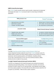
XN62Lxxx4 Functional Description4.1 ARM Cortex M0The Cortex-M0 processor is 32-bit Reduced Instruction Set Computing (RISC) processor introduced by ARM. It has anAMBA AHB-Lite interface and includes a Nested Vector Interrupt Controller (NVIC) component. It also has hardware debugfunctionality. The processor uses Thumb instruction set and is compatible with other ARM Cortex-M profile processor. Itsupports two modes -Thread mode and Handler mode. Handler mode is entered as a result of an exception. An exceptionreturn can only be issued in Handler mode. Thread mode is entered on Reset, and can be entered as a result of anexception return.The below figure shows the functional blocks of processor.PowerManagementInterfaceConnection toDebuggerWakeup InterruptControllerSWD DebugInterfaceInterruptRequest andNMINested VectorInterrupt Controller(NVIC)Cortex-M0Processor CoreDebug SubsystemInternal Bus SystemAHB LITE BusInterfaceCortex-M0Memory andPeripheralsFigure 4-1: Cortex M0 core block diagramARM Cortex-M0 processor provides the following functions and features:• The ARMv6-M Thumb ® instruction set• Thumb-2 technology• ARMv6-M compliant 24-bit System Tick (SysTick) timer• A 32-bit hardware multiplier• The system interface supports little-endian data accesses• The ability to have deterministic, fixed-latency, interrupt handling16 www.xinnovatech.com
XN62Lxxx• Load/store-multiples and multicycle-multiplies that can be abandoned and restarted to facilitate rapid interrupthandling• C Application Binary Interface compliant exception model. This is the ARMv6-M, C Application Binary Interface(C-ABI) compliant exception model that enables the use of pure C functions as interrupt handlers• Low power sleep mode entry using Wait For Interrupt (WFI), Wait For Event (WFE) instructions, or the return frominterrupt sleep-on-exit feature• NVIC that features:– 32 external interrupt inputs, each with four levels of priority– Dedicated Non-Maskable Interrupt (NMI) input.– Support for both level-sensitive and pulse-sensitive interrupt lines– Wake-up Interrupt Controller (WIC), providing ultra-low power sleep mode support.• Debug support– Four hardware breakpoints.– Two watch points.– Program Counter Sampling Register (PCSR) for non-intrusive code profiling.– Single step and vector catch capabilities.• Bus interfaces:– Single 32-bit AMBA-3 AHB-Lite system interface that provides simple integration to all system peripherals andmemory.– Single 32-bit slave port that supports the Debug Access Port (DAP).4.2 Memory MapXN62L memory address space supports up to 4GB size. It’s divided into a few memory segments: boot area, flash memoryarea, SRAM area, private peripheral area, APB peripheral area and AHB peripheral area.The private peripheral area is reserved for M0 core.The AHB peripheral area is 2 MB in size and is divided to allow for up to 128 peripherals. The GPIO ports, the xDSP, and theDMA controller are AHB peripherals.The APB peripheral area is 512 KB in size and each peripheral of either type is allocated with 16 KB. This allows simplifiedaddress decoding for each peripheral. All peripheral register addresses are 32-bit word aligned regardless of their size. Animplication of this is that word and half-word registers must be accessed all at once. For example, it is not possible to read orwrite the upper byte of a word register separately.The boot area is 8 KB size and is used to store MCU bootloader, ISP and IAP function. The user is able to take up to 88 KBflash memory and 16 KB SRAM for application usage. The flash and SRAM apply 32-bit data bus.The following diagram shows memory allocation:www.xinnovatech.com 17
XN62LxxxPrivate peripheralReserved0xE010 00004GBReservedPrivate peripheralReservedAHB peripheral0xFFFF FFFF0xE010 00000xE000 00000x5008 00000x5000 0000SCBNVICSystem TickReservedAHB peripheralxDSPFlashReservedGPIO PIO2GPIO PIO1GPIO PIO0APB peripheral0xE000 EE000xE000 ED000xE000 E1000xE000 E0000xE000 00000x5008 00000x5007 00000x5006 00000x5003 00000x5002 00000x5001 00000x5000 0000ReservedAPB peripheralReserved8KB Boot romReservedReserved16KB SRAMReserved88KB On-chip0x4008 00000x4000 00000x1FFF 20000x1FFF 00000x1FFE 00000x1000 40000x1000 00000x0001 60000x0000 0000Interrupt vectors0x0000 00C00x0000 0000ReservedUART2UART2DAC0ADC2ADC1PWM2PWM1PWM0Comparator 0/1RTCDMASystem controlIO configSPIReservedPMUReserved0x4008 00000x4007 80000x4007 40000x4007 00000x4006 C0000x4006 80000x4006 40000x4006 00000x4005 C0000x4005 80000x4005 40000x4005 00000x4004 C0000x4004 80000x4004 40000x4004 00000x4003 C0000x4003 8000ADC032-bit timer/counter32-bit timer/counter16-bit timer/counter16-bit timer/counterUART1UART0WDTTWS0x4002 40000x4002 00000x4001 C0000x4001 80000x4001 40000x4001 00000x4000 C0000x4000 80000x4000 40000x4000 0000Figure 4-2: Memory allocation diagram18 www.xinnovatech.com
4.3 xDSP CoprocessorXN62LxxxXN62L integrates a mini DSP processor (known as xDSP), which is used to handle the microcontroller’s complex arithmeticoperation. The xDSP is independent from the ARM core and provides a set of access registers interface to ARM software.By calling interface register, the xDSP is able to perform the following predefined functions:• CRC calculation– CRC-CCITT algorithm– CRC-16 algorithm– CRC-32 algorithm• 32-bit divider• Configurable 16~32-bit Sin, Cosin, Arctan operation• Configurable Finite Impulse Response (FIR) filter and Infinite Impulse Response(IIR) filter4.4 System Clock ControllerCompare with other MCU system, XN62L applies very flexible clock system. There are four clock sources in system:External crystal oscillator, Internal RC oscillator, WDT oscillator and external RTC oscillator. The integrated PLL allowssystem running in high frequency with lower clock source. See following figure for an overview of the XN62L clock system.XTALINXTALOUTSYS_OSCSYS_OSC_CLKSYS_PLLCLK_INPLLSystem CLKDIVIDERSystem ClkARM CorePeripheralPCLKSYS_OSC_BYPASSSYS_PLLCLKIN_SELMAIN_CLKIRC_OSCIRC_OSC_CLKMAINCLK_SELSYSAHBCLKCTRLWDT_CLKWDT_OSCWDT_OSC_CLKWDT_CLK_SELINTERNALCLOCKDIVIDERSUART0/1,RTC,SysTickPCLKRTCXINRTCXOUTRTC_OSC1Hz1KHzRTCTimerRTCDIVIDERRTC_SELCLOCKOUTDIVIDERCLOCKOUTOutside-Chip-InsideCLOCKOUT_SELInside-Chip-OutsideFigure 4-3: Clock system block diagramFollowing reset, the XN62L will operate from the Internal RC oscillator until switched by software. This allows systems tooperate without any external crystal and the boot loader code to operate at a known frequency.www.xinnovatech.com 19
XN62LxxxThe Main Clock is operation clock for whole device and can be selected from either of External crystal oscillator, Internal RCoscillator, WatchDog Timer (WDT) oscillator and PLL output.The system clock is divided from main clock and provides to ARM Core and is gated to the various peripherals andmemories by SYSAHBCLKCTRL register. UART0/1/2/3, RTC, and the SysTick timer have individual clock dividers to deriveperipheral clocks from the main clock. The watchdog clock can be derived from the oscillator output or the main clock. Themain clock, and the clock outputs from the IRC, the system oscillator, and the watchdog oscillator can be observed directlyon the CLKOUT pin.4.5 System ResetThe system reset can be triggered by the following events:• The Power-On Reset (POR)• The low level on the RESET# pin• Watchdog Time Out Reset• Brown-Out Detector Reset (BOD)• Software Reset• System Reset from deep power down wake upThe RESET# pin is a Schmitt trigger input pin. Assertion of Reset by any source, once the operating voltage attains a usablelevel, starts the IRC causing reset to remain asserted until the external Reset is de-asserted, the oscillator is running, andthe flash controller has completed its initialization. On the assertion of a reset source external to the Cortex-M0 CPU (POR,BOD reset, External reset, and Watchdog reset), the following processes are initiated:• The IRC starts up. After the IRC-start-up time, the IRC provides a stable clock output.When the internal Reset is removed, the processor begins executing at address 0, which is initially the Reset vector mappedfrom the boot block. At that point, all of the processor and peripheral registers have been initialized to predetermined values.All reset sources are recorded in reset status register.4.6 Nested Vectored Interrupt ControllerThe Nested Vectored Interrupt Controller (NVIC) is an integral part of the Cortex-M0. The tight coupling to the CPU allowsfor low interrupt latency and efficient processing of late arriving interrupts. The major features:• Tightly coupled interrupt controller provides low interrupt latency.• Controls system exceptions and peripheral interrupts.• Supports 32 vectored interrupts.• Four programmable interrupt priority levels with hardware priority level masking.• Software interrupt generation.• Non-Maskable Interrupt (NMI) with configurable source.20 www.xinnovatech.com
XN62LxxxThe following lists the interrupt sources for system and each peripheral function. Each peripheral device may have one ormore interrupt lines to the Vectored Interrupt Controller. Each line may represent more than one interrupt source. There isno significance or priority about what line is connected where, except for certain standards from ARM.Table 4-1: Vectored Interrupt sources and vector listExceptionIRQOffset Addr.Exception Type Priority DescriptionNumberNumberin VectorTable0x00Initial SP Value1 0x04 Reset -3 the Highest2 -14 0x08 NMI -23 -13 0x0C HardFault -110~4 0x10~0x28 Reserved11 -5 0x2C SVCall Configurable(1)13~12 0x30~0x34 Reserved14 -2 0x38 PendSV Configurable(1)15 -1 0x3C SysTick Configurable(1)16 0 0x40 wake-upinterrupt 017 1 0x44 wake-upinterrupt 118 2 0x48 wake-upinterrupt 219 3 0x4C wake-upinterrupt 320 4 0x50 PWM 0 faultinterrupt21 5 0x54 PWM 1 faultinterrupt22 6 0x58 PWM 2 faultinterruptConfigurable(2)Configurable(2)Configurable(2)Configurable(2)Configurable(2)Configurable(2)Configurable(2)Connected to a PIO input pin serving as wake-uppin when the part is in Deep-sleep mode; Interrupt0 correspond to PIO0_0, PIO0_4 and PIO0_8.Connected to a PIO input pin serving as wake-uppin when the part is in Deep-sleep mode; Interrupt1 correspond to PIO0_1, PIO0_5 and PIO0_9.Connected to a PIO input pin serving as wake-uppin when the part is in Deep-sleep mode; Interrupt2 correspond to PIO0_2, PIO0_6 and PIO0_10.Connected to a PIO input pin serving as wake-uppin when the part is in Deep-sleep mode; Interrupt3 correspond to PIO0_3, PIO0_7 and PIO0_11.23 7 0x5C PWM2 Configurable(2)24 8 0x60 ADC1 Configurable(2)25 9 0x64 ADC2 Configurable(2)26 10 0x68 UART2 Configurable(2) Transmit Holding Register Empty (THRE)Transmit Holding Register overrun(THROE)Receive Buffer Full(RBRS)Receive Buffer Overrun(RBROE)www.xinnovatech.com 21
XN62Lxxx27 11 0x6C UART3 Configurable(2) Transmit Holding Register Empty (THRE)Transmit Holding Register overrun(THROE)Receive Buffer Full(RBRS)Receive Buffer Overrun(RBROE)28 12 0x70 TWS Configurable(2) SI (state change)29 13 0x74 CT16B0 Configurable(2) Match 3 to 0Capture 3 to 030 14 0x78 CT16B1 Configurable(2) Match 3 to 0Capture 3 to 031 15 0x7C CT32B0 Configurable(2) Match 3 to 0Capture 3 to 032 16 0x80 CT32B1 Configurable(2) Match 3 to 0Capture 3 to 033 17 0x84 SPI Configurable(2) Tx FIFO half empty Rx FIFO half fullRx TimeoutRx Overrun34 18 0x88 UART0 Configurable(2) Transmit Holding Register Empty (THRE)Transmit Holding Register overrun(THROE)Receive Buffer Full(RBRS)Receive Buffer Overrun(RBROE)35 19 0x8C UART1 Configurable(2) Transmit Holding Register Empty (THRE)Transmit Holding Register overrun(THROE)Receive Buffer Full(RBRS)Receive Buffer Overrun(RBROE)36 20 0x90 Comparator Configurable(2) Comparator 0/1 interrupt37 21 0x94 ADC0,1 Configurable(2) A/D Converter end of conversion38 22 0x98 WDT Configurable(2) Watchdog interrupt (WDINT)39 23 0x9C BOD Configurable(2) Brown-out detect40 24 0xA0 PWM0 Configurable(2) PWM0 interrupt41 25 0xA4 PIO0 Configurable(2) GPIO interrupt status of port 042 26 0xA8 PIO1 Configurable(2) GPIO interrupt status of port 143 27 0xAC PIO2 Configurable(2) GPIO interrupt status of port 244 28 0xB0 PWM1 Configurable(2) PWM1 interrupt45 29 0xB4 DMA Configurable(2) DMA request interrupt46 30 0xB8 RTC Configurable(2) RTC interrupt47 31 0xBC DAC Configurable(2) D/A converter interrupt1. See SCB control register SHPR2-SHPR3.2. See IPR0~IPR7 of NVIC.22 www.xinnovatech.com
4.7 IO ConfigurationXN62LxxxTo do pin multiplex for different application requirement, XN62L is designed to have one IOCON register for each pinassignment. The I/O configuration registers control the electrical characteristics of the pads. The following features areprogrammable:• Pin function– General IO, Peripheral pin, AD pin• Pin mode– Internal pull-up, open-drain mode• Pin drive– Normal drive, high drive• Analog input or digital mode for pads hosting the ADC inputs• Digital IO pin glitch filter4.8 Advanced PWM moduleThe XN62Lxx has up to three independent Pulse Width Modulator (PWM0, PWM1 and PWM2) modules. Each PWMmodule can be configured as three complementary pairs, 8 independent PWM signals or their combinations, such as onecomplementary and four independent. Both Edge- Aligned and Center-Aligned synchronous pulse width control, from zeroto 100 percent modulation are supported.A 15-bit common PWM counter is applied for each PWM module. PWM resolution is one clock period for Edge-Alignedoperation and two clock periods for Center-Aligned operation. The clock period is dependent on clock source frequency ofPWM_PCLK(System Clock) and programmable prescaler.When generating complementary PWM signals, the module features automatic deadtime insertion to PWM output pairs.Each PWM output can be controlled by PWM generator, timer, conversion results of ADC, GPIO pins, or software manuallyand separate top and bottom output polarity control. Asymmetric PWM output is able to change PWM duty cyclealternatively at every half cycle without software involvement.4.8.1 Features• Two PWM modules• PWM Operation Clock runs at System Clock• Total up 24 PWM signals– all independent– complementary pairs– mix independent and complementary• Features of complementary channel operation– separate deadtime insertions for rising and falling edgeswww.xinnovatech.com 23
XN62Lxxx– separate top and bottom pulse width correction via software– asymmetric PWM output within Center Align operation– separate top and bottom polarity control• Edge- or Center-Aligned PWM signals• 15 bits of resolution• Half-cycle reload capability• Integral reload rates from 1 to 16• Individual software controlled PWM output• Programmable fault protection• PWM compare output polarity control• PWM output polarity control• Push-Pull and Open Drain modes are available on PWM pins• Write-protected registers• Selectable PWM supply source for each complementary PWM signal pair– PWM generator– external GPIO pin– internal timer channel– ADC conversion result, taking into account values set in ADC high and low limit registersIf all three PWM pairs are driven by any one of the above sources, the following features are disabled:• PWM sync pulse is not applicable• PWM reload registers will have no effect4.8.2 Block DiagramThe PWMn (n=0,1,2) block diagram is illustrated in Figure 4-4..24 www.xinnovatech.com
XN62LxxxPCLKEdge or Center AlignControlPrescalerPWM CounterModulusPWM CounterPWM ControlSources-ADC-GPIO-TimerPWM Value Register 0Compare Unit 0PWM 0PWM Value Register 1Compare Unit 1PWM 1PWM Value Register 2PWM Value Register 3PWM Value Register 4PWM Value Register 5Compare Unit 2Compare Unit 3Compare Unit 4Compare Unit 5MUX/SWAP/DEADTIMEInsertion andOutput ControlPWM Fault Protection and Channel MaskPolarity ControlPWM 2PWM 3PWM 4PWM 5PWM Value Register 6Compare Unit 6PWM 6PWM Value Register 7Compare Unit 7PWM 7PWM Compare OutputPolarity ControlSoftware Controland Output ModeSettingFliters Fault Input [3:0]Figure 4-4: PWMn(n=0,1,2) Block Diagram4.9 GPIOXN62L provides up to 55 GPIOs (PIO0: 0~31; PIO1: 0~6; PIO2: 0~15) with QFP64 package. The following are the majorfeatures:• Digital ports can be configured as input or output by software.• Read and write data operations from/to the port pins are maskable.• Bit-level set and clear registers allow a single-instruction set or clear of any number of pins in one port.• Bit-level invert registers allow inverting the output of any number of pins in one port.• Each individual port pin can serve as external interrupt input.• Interrupts can be configured on single falling or rising edges and on both edges.• Individual interrupt levels can be programmed.• All GPIO pins are configured as inputs (with pull-up resistors enabled) after reset.www.xinnovatech.com 25
XN62Lxxx4.10 ADC/DACXN62L provides up to three 12-bit high resolution ADCs and one 10-bit DAC for customer application requirements. Thefollowing are the major features:• 1MHz 12-bit AD sampling rate and up to 8 channels.• Supports Power-down mode.• ADC Measurement range 0 to 3.3V.• Burst ADC conversion mode for single or multiple inputs.• Optional ADC conversion on transition on input pin or Timer Match signal.• Individual ADC result registers for each A/D channel to reduce interrupt overhead.• Max 1MHz DA conversion rate4.11 ComparatorTwo embedded comparators are incorporated on-chip to compare the voltage levels on external pins or against internalvoltages/DA output. Up to six voltages on external pins and two internal reference voltages or DA output are selectable oneach comparator. Additionally, four of the external input voltages can be selected to drive an input common on bothcomparators in case identical voltages are required on both comparators. The major features as the following:• Up to six selectable external sources per comparator; fully configurable on either positive or negative comparator inputchannels.• The DA output and internal reference voltage selectable on both comparators; configurable on either positive or negativecomparator input channels.• 32-stage voltage ladder internal reference voltage selectable on both comparators; configurable on either positive ornegative comparator input channels.• Voltage ladder source voltage is selectable from an external pin or the 3.3 V voltage rail if the external power source isnot available.• Voltage ladder can be separately powered down for applications only requiring the comparator function.• Individual comparator interrupts connected to I/O pins, common interrupt connected to NVIC.• Edge and level comparator outputs connect to two timers allowing edge tick counting while a level match has beenasserted.4.12 UART InterfaceXN62L provides four UART peripherals: UART0, UART1, UART2 and UART3. All are able to support infraredcommunications by changing to IrDA configuration. The following are the major features:• Fixed data format for data communication: 1 start bit, 8 data bits, 2 stop bits, no parity and hardware flow control.• Support baudrate auto-detection.26 www.xinnovatech.com
4.13 SPI InterfaceXN62LxxxXN62L provides an extended SPI interface which is compliant to standard SPI and 4-wire SSI bus. It can interact withmultiple masters and slaves on the bus. Only a single master and a single slave can communicate on the bus during a givendata transfer. Data transfers are in principle full duplex, with frames of 4 bit to 16 bit of data flowing from the master to theslave and from the slave to the master. The following are the major features:• Compatible with SPI and 4-wire TI SSI buses• Synchronous Serial Communication• Master or slave operation• Eight-frame FIFOs for both transmit and receive• 4-bit to 16-bit frame4.14 Two-Wire Serial (TWS) InterfaceTWS is a kind of two wires serial communication interface, which is compatible to I 2 C-bus. It is able to support I 2 C bothmaster and slave mode. The following are the major features of TWS interface:• Standard I 2 C-compliant bus interfaces may be configured as Master, Slave, or Master/Slave.• Arbitration is handled between simultaneously transmitting masters without corruption of serial data on the bus.• Programmable clock allows adjustment of TWS transfer rates.• Data transfer is bidirectional between masters and slaves.• Serial clock synchronization allows devices with different bit rates to communicate via one serial bus.• Serial clock synchronization is used as a handshake mechanism to suspend and resume serial transfer.• Supports Fast-mode Plus, up to 3MHz.• Optional recognition of up to four distinct slave addresses.• Monitor mode allows observing all TWS-bus traffic, regardless of slave address.• TWS-bus can be used for test and diagnostic purposes.• The TWS block contains a standard I 2 C compliant bus interface with two pins.pull-upresistorpull-upresistorSDACompatible I 2 C busSCLSDASCLXN62LxxxOTHER XN62LxxxOTHER I 2 C CompatibleDEVICEFigure 4-5: TWS application bus configurationwww.xinnovatech.com 27
XN62Lxxx4.15 Enhanced General Timers/CountersXN62L has two multi-function 16-bit counters/timers and two multi-function 32-bit counters/timers. Each of counter/timer’smain features are as follows:• Programmable 16-bit prescaler to timer/counter clock.• Normal Counter or timer operation plus:– Edge count mode– Gated count Mode– Quadrature count mode– Trigger count Mode– Signed count mode• Four capture channels that can take a snapshot of the timer value when an input signal transits. A capture event mayalso optionally generate an interrupt.• The timer and prescaler may be configured to be cleared on a designated capture event. This feature permits easypulse-width measurement by clearing the timer on the leading edge of an input pulse and capturing the timer value onthe trailing edge.• Four match registers that allow:– Continuous operation with optional interrupt generation on match.– Stop timer on match with optional interrupt generation.– Reset timer on match with optional interrupt generation.• Four(32-bit timer)/two(16-bit timer) external outputs corresponding to match registers with the following capabilities:– Set LOW on match.– Set HIGH on match.– Toggle on match.– Do nothing on match.• For each timer, up to four match registers can be configured as PWM allowing it to use up to two match outputs as singleedge controlled PWM outputs.28 www.xinnovatech.com
XN62LxxxCAPTURE REGISTER 3CAPTURE REGISTER 2CAPTURE GEGISTER 1CAPTURE REGISTER 0MATCH REGISTER 3MATCH REGISTER 2MATCH REGISTER 1MATCH REGISTER 0CAPTURE CONTROL REGISTERMATCH CONTROL REGISTERENTERNAL MATCH REGISTERINTERRUPT REGISTERCONTROL==LOAD[3:0]==MATxINTERRUPTCAPxTIMER CONTROLREGISTERReset/EnableTIMER COUNTER+ -COUNT/Edge CNTQUADCNTGATECNTTRIGGERCNTSIGNEDCNTPRISECSOURCE SELMAXVALPRESCALE REGISTERPRESCALECOUNTERCAPxC16B MATC32BMATPCLKFigure 4-6: Counter/timer block diagram4.16 RTC TimerBy counting 1 Hz/1KHz clock from reference time, 32-bits RTC timer is used to perform real time clock function. RTCfeatures are showed as:• Dedicated 32 kHz ultra low power oscillator.• Uses 1 Hz clock to count in one second intervals.• 32-bit RTC counter.• Alarm and wake up functions to system4.17 DMA ControllerThe DMA controller is a very low-gate-count DMA compatible with the AMBA. AHB-Lite protocol for DMA transfers. TheDMA registers are programmed through the APB interface. The DMA Features are as the following:• Single AHB-Lite master for transferring data using a 32-bit address bus and 32-bit data bus.• 28 DMA channels.• Dedicated handshake signals and programmable priority level for each channel.www.xinnovatech.com 29
XN62Lxxx• Each priority level arbitrates using a fixed priority that is determined by the DMA channel number.• Supports memory-to-memory, memory-to-peripheral, and peripheral-to-memory transfers.• Supports multiple DMA cycle types and multiple DMA transfer widths.• Each DMA channel can access a primary and an alternate channel control data structure.• The channel control data is stored in system memory in little-endian format.• Performs all DMA transfers using single AHB-Lite transfers. Burst transfers are not supported.• The destination data width is equal to the source data width.• The number of transfers in a single DMA cycle can be programmed from 1 to 1024.• The transfer address increment can be greater than the data width.4.18 Flash Memory ISP/IAP and High Security FeaturesXN62L supports both In-System-Programming (ISP) and In-Application-Programming (IAP) for application code flashmemory. The user can call ISP/IAP functions via XN62L Bootloader interface. See details for ISP/IAP protocol in usermanual.XN62L offers 128 bits password security feature to prevent unauthorized users from writing/reading the contents of the flashmemory array. Further, the user application memory, flash and SRAM, can be split to two areas and protected by different128 bits password.0x0001 5FFFFlash Memory(88KB)0x10003000SRAM(12KB)Access Control byB AreaB AreaPassword B (128 bits)0x000x xxxx0x1000 xxxxOpen AreaA Area0x1000 0000Password A (128 bits)0x0000 0000Figure 4-7: Password security mechanismAs described in Figure 4-7, A area and B area memory access via SWD, software are controlled by 128 bits A and B passwords. Thefollowing are main features under password protection:1. Software running on B area is able to read A/B/open area and write B area/open area.2. Software running on A area is able to call function in B area, but no read/write.3. Software running on A area is able to read/write A and open area.4. No SWD.30 www.xinnovatech.com
4.19 Watchdog TimerXN62LxxxThe watchdog timer is used to reset/interrupt microcontroller when user application is running into error and fail to feedwatchdog timer. With programmable timer, the user can set timer in wide range for different application. XN62L WDT hasthe following major features:• Independent WDT oscillator clock source with flexible frequency set from 0.3MHz to 2.2MHz (typical)• Watchdog can trigger both reset and interrupt• Support power saving mode4.20 Power ManagementThe XN62L support a variety of power saving control features. In Active mode, when the microcontroller is running, powerand clocks to selected peripherals can be optimized for power consumption. In addition, there are three special modes ofprocessor power reduction: Sleep mode, Deep-sleep mode, and Power-down mode.4.20.1 Sleep ModeIn Sleep mode, the system clock to the ARM Cortex-M0 core is stopped, and execution of instructions is suspended untileither a reset or an enabled interrupt occurs.For peripheral functions, if selected to be clocked in the SYSAHBCLKCTRL register, continue operation during Sleep modeand may generate interrupts to cause the processor to resume execution. Sleep mode eliminates dynamic power used bythe processor itself, memory systems and their related controllers, and internal buses. The processor state and registers,peripheral registers, and internal SRAM values are maintained, and the logic levels of the pins remain static.4.20.2 Deep-sleep ModeIn Deep-sleep mode, the system clock to the processor is disabled as in Sleep mode. All analog blocks are powered down,except for the BOD circuit and the watchdog oscillator, which must be selected or deselected during Deep-sleep mode in thePDSLEEPCFG register. The RTC and the RTC oscillator are operating in Deep-sleep mode unless the RTC is powereddown. Deep-sleep mode eliminates all power used by the flash, analog peripherals and all dynamic power used by theprocessor itself, memory systems and their related controllers, and internal buses. The processor state and registers,peripheral registers, and internal SRAM values are maintained, and the logic levels of the pins remain static.4.20.3 Power-down ModeIn Power-down mode, power and clocks are shut off to the entire microcontroller with the exception of the WAKEUP pin. Themicrocontroller is blocked from entering Power-down mode when the WDLOCKDP bit is set to one in the WDMODEregister.If the RTC is enabled before entering Power-down mode, the RTC and the RTC oscillator continue to run in Power-downmode. If the RTC is not needed in Power-down mode, disable the RTC to minimize power consumption.During Power-down mode, the contents of the SRAM and registers are not retained except for a small amount of data whichcan be stored in the four 32-bit general purpose registers of the PMU block.www.xinnovatech.com 31
XN62Lxxx4.21 SWD InterfaceXN62L provides SWD interface which supports standard ARM Serial Wire Debug mode. It allows:• Direct debug access to all memories, registers, and peripherals.• No target resources are required for the debugging session.• Four breakpoints. Four instruction breakpoints, which can also be used to remap instruction addresses for code patches.Two data comparators which can be used to remap addresses for patches to literal values.• Two data watch points, which can also be used as trace triggers.32 www.xinnovatech.com
XN62Lxxx5 Electrical Characteristics5.1 Absolute Maximum RatingsTable 5-1: Absolute ratingsSymbol Parameter Min Max UnitV SS -0.3 VPower SupplyV DD(3V3) +3.0 +3.6 VV SSIO -0.3 VV DD(IO) +3.0 +3.6 VInput Voltage V IN -0.5 +3.6 VOscillator Frequency 1/t clcl 500K 16M HzRTC 1/t clcl 32.768K HzOperating Temp. T A -40 +85 °CStorage Temp. T S -65 +150 °CMaximum Current into V DD I DD 120 mAMaximum Current out V SS I SS 120 mAMaximum Current sunk by a IO pin 40 mAMaximum Current sourced by a IO pin 40 mAMaximum Current sunk by total IO pins 100 mAMaximum Current sourced by total IO pins 100 mAElectrostatic discharge voltage V ESD -4000 +4000 Vwww.xinnovatech.com 33
XN62Lxxx5.2 DC Electrical CharacteristicsTable 5-2: General static characteristicsT amb = -40°C to +85°C, unless otherwise specified.Symbol Parameter Conditions Min Typ[1] Max UnitV DD(IO)input/output supplyvoltageon pin V DD(IO) 3.0 3.3 3.6 VV DD(3V3) supply voltage (3.3 V) 3.0 3.3 3.6 VI DD supply current Active mode; V DD(3V3) =3.3 V; T amb =25°C; code while(1){} executed from flash;all peripherals disabled:CCLK = 10 MHz - 3.7 - mACCLK = 20 MHz - 5.3 - mASleep mode; V DD(3V3) = 3.3 V; T amb =25°C; all peripherals disabledCCLK = 10 MHz - 1.2 - mACCLK = 20 MHz - 2.8 - mADeep-sleep mode; V DD(3V3) = 3.3 V; T amb =25°C- 50 - uAPower-down mode; V DD(3V3) = 3.3 V; T amb =25°C- 10 - uAStandard port pins, RESET#I ILI IHI OZLOW-level inputcurrentHIGH-level inputcurrentOFF-state outputcurrentV I =0V; - - 1 uAV I =V DD(IO) - - 1 uAV O =0V; VO =V DD(IO) - - 1 uAV I input voltage pin configured to provide a digital0 - V DD(IO) Vfunction [2][3][4]V O output voltage output active 0 - V DD(IO) VV IHV ILHIGH-level inputvoltageLOW-level inputvoltage0.7V DD(IO) - - V- - 0.3V DD(IO) VV hys hysteresis voltage - 0.4 - VV OHV OLHIGH-level outputvoltageLOW-level outputvoltageI OH=~4mA 2.4 - - VI OL =4 mA - - 0.4 VI OHHIGH-level outputV OH =2.4 V Normal-drive pins; low3.9 7.8 12.9 mAcurrentmode [5]Normal-drive pins; high mode [5] 7.7 15.6 25.8 mA34 www.xinnovatech.com
XN62LxxxHigh-drive pins; low mode [6] 17.4 35.1 58.1 mAHigh-drive pins; high mode [6] 23.1 46.8 77.5 mAI OLLOW-level outputV OL =0.4 V Normal-drive pins; low3.4 5.4 7.4 mAcurrentmode [5]I OHSI OLSHIGH-levelshort-circuit outputcurrentLOW-level short-circuitoutput currentNormal-drive pins; high mode [5] 6.7 10.7 14.7 mAHigh-drive pins; low mode [6] 13.4 21.5 29.4 mAHigh-drive pins; high mode [6] 20.1 32.2 44.1 mAV OH =0V [7] - - 45 mAV OL =V DD [7] - - 50 mAI pu pull-up current V I =0V ~50 ~80 ~100 uATWS-bus pins (PIO0_10 and PIO0_11)V IHV ILHIGH-level inputvoltageLOW-level inputvoltage0.7V DD(IO) - - V- - 0.3V DD(IO) VV hys hysteresis voltage - 0.05V DD(IO) - VV OLLOW-level outputvoltageI OLS =20 mA - - 0.4 VI LI input leakage current V I =V DD(IO) [8] - 2 4 uAV I =5V - 10 22 uAC iOscillator pinscapacitance for eachI/O pinon pins PIO0_10 and PIO0_11 - - 8 pFV i(xtal) crystal input voltage 0 1.8 1.95 VV o(xtal) crystal output voltage 0 1.8 1.95 V[1] Typical ratings are not guaranteed. The values listed are at room temperature (25°C), nominal supply voltages.[2] Including voltage on outputs in 3-state mode.[3] V DD(3V3) and V DD(IO) supply voltages must be present.[4] 3-state outputs go into 3-state mode when V DD(IO) is grounded.[5] Normal-drive output mode applies to all GPIO pins except pins PIO0_12, PIO0_27, PIO0_28, PIO0_29.[6] High-drive output mode available on pins PIO0_12, PIO0_27, PIO0_28, PIO0_29.[7] Allowed as long as the current limit does not exceed the maximum current allowed by the device.[8] To VSS.5.2.1 BOD Static CharacteristicsTable 5-3: BOD static characteristicsT amb = 25°C.Symbol Parameter Conditions Min Typ Max Unitwww.xinnovatech.com 35
XN62LxxxV th threshold voltage Interrupt levelassertion - 2.828 - Vde-assertion - 2.929 - VReset levelassertion - 2.624 - Vde-assertion - 2.759 - V5.2.2 ADC CharacteristicsTable 5-4: ADC static characteristicsT amb = -40°C to +85°C unless otherwise specified; V DD(3V3) = 3.0 V to3.6 V.Symbol Parameter Conditions Min Typ[1] Max Unit- Resolution 12 BitV IA analog input voltage 0 - V DD(3V3) VC in analog input capacitance - - 30(1) pFDNL differential linearity error [2][3][4] - -1 ±0.9 1.5 LSBINL integral non-linearity [2][5] - -3 ±1 3 LSBE O offset error [2][6] - - - 1 LSBE G gain error [2][7] - - - 3 LSBE T absolute error [2][8] - - - 3 LSBCLK Clock frequency 0.6 16 MHzt ADC Conversion Time 16 Clockf c(ADC) ADC conversion frequency - - 1000 KSPSNote:[1] Typical ratings are not guaranteed. The values listed are at room temperature (25°C), nominal supply voltages.[2] Conditions: V SS = 0 V, V DD(3V3) = 3.3 V.[3] The ADC is monotonic, there are no missing codes.[4] The differential linearity error (DNL) is the difference between the actual step width and the ideal step width.[5] The integral non-linearity (INL) is the peak difference between the center of the steps of the actual and the ideal transfer curve after appropriate adjustment of gainand offset errors.[6] The offset error (E O) is the absolute difference between the straight line which fits the actual curve and the straight line which fits the ideal curve.[7] The gain error (E G) is the relative difference in percent between the straight line fitting the actual transfer curve after removing offset error, and the straight line36 www.xinnovatech.com
XN62Lxxxwhich fits the ideal transfer curve.[8] The absolute error (E T) is the maximum difference between the center of the steps of the actual transfer curve of the non-calibrated ADC and the ideal transfercurve.www.xinnovatech.com 37
XN62Lxxx5.3 AC Electrical Characteristics5.3.1 Flash MemoryTable 5-5: Flash memoryT amb = -40°C to +85°C; V DD (3V3) over specified ranges.Symbol Parameter Conditions [1] Min - Max Unitt erase erase time for one sector (1K Bytes) 5 mst prog programming time one word (4 bytes) [1] - 20 usN cyc endurance [2] 100,000 - cyclest ret retention time 100 - yearsNote:[1] Erase and programming times are valid over the lifetime of the device (minimum 20000 cycles).[2] Number of program/erase cycles.5.3.2 External Clockt CHCLt CLCXT cy(clk)t CHCXt CLCHFigure 5-1: External clock timingTable 5-6: External clockT amb = -40°C to +85°C; V DD(3V3) over specified ranges.[1]Symbol Parameter Conditions Min Typ[2] Max Unitf osc oscillator frequency 0.4 - 16 MHzt cy(clk) clock cycle time 40 - 1000 nst CHCX clock HIGH time t cy(clk) x 0.4 - - nst CLCX clock LOW time t cy(clk) x 0.4 - - nst CLCH clock rise time - - 5 nst CHCL clock fall time - - 5 nsNote:[1] Parameters are valid over operating temperature range unless otherwise specified.[2] Typical ratings are not guaranteed. The values listed are at room temperature (25 °C), nominal supply voltages.5.3.3 RTC Clockt CHCLt CLCXT cy(clk)t CHCXt CLCH38 www.xinnovatech.com
XN62LxxxFigure 5-2: RTC clock timingTable 5-7: RTC clockT amb = -40°C to +85°CSymbol Parameter Conditions Min Typ[2] Max Unitf osc oscillator frequency - 32.768 - kHzt cy(clk) clock cycle time 40 - 1000 nst CHCX clock HIGH time t cy(clk) x 0.4 - - nst CLCX clock LOW time t cy(clk) x 0.4 - - nst CLCH clock rise time - - 5 nst CHCL clock fall time - - 5 ns5.3.4 SPI InterfaceTable 5-8: Dynamic characteristics: SPI pins in SPI modeT amb = 25°C.Symbol Parameter Conditions Min Max Unitt cy(clk) clock cycle time when only transmitting [1] - nswhen only receiving -SPI mastert DS data set-up time in SPI mode [2] 15 - nst DH data hold time in SPI mode [2] 0 - nst v(Q) data output valid time in SPI mode [2] - 10 nst h(Q) data output hold time in SPI mode [2] 0 - nsSPI slavet DS data set-up time in SPI mode [3][4] 0 - nst DH data hold time in SPI mode [3][4] 3xt cy(PCLK) + 4 - nst v(Q) data output valid time in SPI mode [3][4] - 3 x t cy(PCLK) + 11 nst h(Q) data output hold time in SPI mode [3][4] - 2 x t cy(PCLK) + 5 nsNote:[1] t cy(clk) = (SPICLKDIV x (1 + SCR) x CPSDVSR) / f main. The clock cycle time derived from the SPI bit rate t cy(clk) is a function of the main clock frequency fmain, theSPI peripheral clock divider (SPICLKDIV), the SPI SCR parameter (specified in the SPI0CR0 register), and the SPI CPSDVSR parameter (specified in the SPI clockprescale register).[2] T amb = -40 °C to + 85 °C; VDD (3V3) = 3.0 V to 3.6 V; V DD(IO) = 3.0 V to 3.6 V.[3] t cy(clk) = 12 x t cy(PCLK).[4] T amb = 25 °C; V DD(3V3) = 3.3 V; V DD(IO) = 3.3 V.www.xinnovatech.com 39
XN62Lxxxtcy(clk) tclk(H) tclk(L)SCK (CPOL = 0)SCK (CPOL = 1)tv(Q)th(Q)MOSIDATA VALIDDATA VALIDtDStDHCPHA = 1MISODATA VALIDDATA VALIDtv(Q)th(Q)MOSIDATA VALIDDATA VALIDtDStDHCPHA = 0MISODATA VALIDDATA VALIDFigure 5-3: SPI master timing in SPI modetcy(clk) tclk(H) tclk(L)SCK (CPOL = 0)SCK (CPOL = 1)tDStDHMOSIDATA VALIDDATA VALIDCPHA = 1tv(Q)th(Q)MISODATA VALIDDATA VALIDtDStDHMOSIDATA VALIDDATA VALIDtv(Q)th(Q)CPHA = 0MISODATA VALIDDATA VALIDFigure 5-4: SPI slave timing in SPI mode5.3.5 TWSTable 5-9: Dynamic characteristic: TWS-bus pinsT amb = -40°C to +85 °C [1]Symbol Parameter Conditions Min Max Unitf SCL SCL clock frequency Standard-mode 0 100 kHz40 www.xinnovatech.com
XN62LxxxFast-mode 0 400 kHzFast-mode Plus 0 1 MHzt f fall time [3][4][5][6] of both SDA and SCL signals- 300 Max nsStandard-mode ConditionsFast-mode 20 + 0.1 Cb 300 nsFast-mode Plus - 120 nst LOW LOW period of the SCL clock Standard-mode 4.7 sFast-mode 1.3 sFast-mode Plus 0.5 st HIGH HIGH period of the SCL clock Standard-mode 4.0 sFast-mode 0.6 sFast-mode Plus 0.26 st HD;DAT data hold time [2][3][7] Standard-mode 0 sFast-mode 0 sFast-mode Plus 0 st SU;DAT data set-up time [8][9] Standard-mode 250 nsFast-mode 100 nsFast-mode Plus 50 nsNote:[1] Parameters are valid over operating temperature range unless otherwise specified.[2] t HD;DAT is the data hold time that is measured from the falling edge of SCL; applies to data in transmission and the acknowledge.[3] A device must internally provide a hold time of at least 300 ns for the SDA signal (with respect to the V IH(min) of the SCL signal) to bridge the undefined region ofthe falling edge of SCL.[4] C b = total capacitance of one bus line in pF. If mixed with high speed mode devices, faster fall times are allowed.[5] The maximum t f for the SDA and SCL bus lines is specified at 300 ns. The maximum fall time for the SDA output stage t f is specified at 250 ns. This allowsseries protection resistors to be connected in between the SDA and the SCL pins and the SDA/SCL bus lines without exceeding the maximum specified t f.[6] In Fast-mode Plus, fall time is specified the same for both output stage and bus timing. If series resistors are used, designers should allow for this whenconsidering bus timing.www.xinnovatech.com 41
XN62Lxxx[7] The maximum t HD;DAT could be 3.45 s and 0.9 s for Standard-mode and Fast-mode but must be less than the maximum of t VD;DAT or t VD;ACK by a transition time.This maximum must only be met if the device does not stretch the LOW period (t LOW) of the SCL signal. If the clock stretches the SCL, the data must be valid by theset-up time before it releases the clock.[8] t SU;DAT is the data set-up time that is measured with respect to the rising edge of SCL; applies to data in transmission and the acknowledge.[9] A Fast-mode TWS-bus device can be used in a Standard-mode TWS-bus system but the requirement t SU;DAT = 250 ns must then be met. This will automaticallybe the case if the device does not stretch the LOW period of the SCL signal. If such a device does stretch the LOW period of the SCL signal, it must output the nextdata bit to the SDA line t r(max) + t SU;DAT = 1000 + 250 = 1250 ns (according to the Standard-mode TWS-bus specification) before the SCL line is released. Also theacknowledge timing must meet this set-up time.tftSU;DATSDA70%30%70%30%tVD;DATtHD;DATtHIGHSCL70%30%70%30%70%30%70%30%S1/fSCLtLOWFigure 5-5: TWS-bus pins clock timing42 www.xinnovatech.com
XN62Lxxx6 Ordering InformationPart No. Operation Voltage Flash(Byte) Ram(Byte) Temperature Range PackageXN62L912-QB 3.3V 88K 16K Industrial LQFP-64XN62L408-QB 3.3V 64K 12K Industrial LQFP-48www.xinnovatech.com 43
XN62Lxxx7 Package DimensionLQFP64: plastic low profile quad flat package; 64 leads; body 10 x 10 x 1.4 mmycX6449148eEH EAA2A1(A3)bpLpƟL1633detail X1732ebpDH DItem Min. Typ. Max. Unit Item Min. Typ. Max. Unit Item Min. Typ. Max. UnitA 1.6 mm c 0.09 0.20 mm H E 11.85 12.20 mmA1 0.05 0.20 mm D 9.9 10.1 mm L 1 mmA2 1.35 1.45 mm E 9.9 10.1 mm L p 0.75 0.45 mmA3 0.25 mm e 0.5 mm y 0.1 mmb p 0.17 0.27 mm H D 11.85 12.20 mm θ 0 3.5 7o44 www.xinnovatech.com
XN62LxxxLQFP48: plastic low profile quad flat package; 48 leads; body 7 x 7 x 1.4 mmcyX4813711pin 1 index36eEH EAA2A1(A3)ƟLp12125bpdetail XL113 2416ebpH DDItem Min. Typ. Max. Unit Item Min. Typ. Max. Unit Item Min. Typ. Max. UnitA 1.6 mm c 0.09 0.20 mm H E 8.80 9.20 mmA1 0.05 0.20 mm D 6.9 7.1 mm L 1 mmA2 1.35 1.45 mm E 6.9 7.1 mm L p 0.75 0.45 mmA3 0.25 mm e 0.5 mm y 0.1 mmb p 0.17 0.27 mm H D 8.80 9.20 mm θ 0 3.5 7owww.xinnovatech.com 45
XN62Lxxx8 Revision HistoryRevision Description Date1.0 Initial Release. Apr. 20121.1 Revised Table 5 2: General static characteristics. Aug. 201246 www.xinnovatech.com