ION MODULATED ORGANIC TRANSISTORS - Doria
ION MODULATED ORGANIC TRANSISTORS - Doria
ION MODULATED ORGANIC TRANSISTORS - Doria
- No tags were found...

Create successful ePaper yourself
Turn your PDF publications into a flip-book with our unique Google optimized e-Paper software.
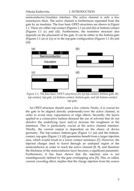
Nikolai Kaihovirta1. INTRODUCT<strong>ION</strong>semiconductor/insulator interface. The active channel is only a fewmonolayers thick. The active channel is furthermore separated from thegate by an insulator. The four basic OFET-structures are shown in Figure1.1. These are either top-contact (Figures 1.1 (a) and (b)) or bottom-contact(Figures 1.1 (c) and (d)). Furthermore, the transistor structure alsodepends on the placement of the gate. It can be either in the bottom-gate(Figures 1.1 (a) or (c)) or in the top-gate configuration (Figures 1.1 (b) and(d)).Figure 1.1. The four basic OFET-structures are (a) top-contact, bottom-gate, (b)top-contact, top-gate, (c) bottom-contact, bottom-gate, and (d) bottom-contacttop-gate.An OFET-structure should meet a few criteria. Firstly, it is crucial forthe gate to be aligned directly underneath/over the active channel, inorder to avoid stray capacitances or edge effects. Secondly, the layersapplied in a consecutive fashion demand the use of solvents that do notdissolve the underlying layer and/or increase the roughness at theinterfaces. This is particularly crucial at the active channel interface.Thirdly, the current output is dependent on the choice of devicegeometry. The top-contact, bottom-gate (Figure 1.1 (a)) and the bottomcontact,top-gate (Figure 1.1 (d)) geometries benefit from a larger injectionarea, which would result in a lower contact resistance [7]. However, theinjected charges need to travel through an undoped region of thesemiconductor in order to reach the active channel [8, 9], and thereforethe thickness of the semiconductor layer becomes a significant parameter.Furthermore, it has been shown that the injection area is notunambiguously defined by the gate overlapping area [9]. This, so called,current crowding effect, implies that the charge injection from the source3