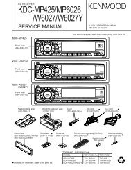
SV-210_211_213_215_2.. - Page de test
SV-210_211_213_215_2.. - Page de test
SV-210_211_213_215_2.. - Page de test

You also want an ePaper? Increase the reach of your titles
YUMPU automatically turns print PDFs into web optimized ePapers that Google loves.
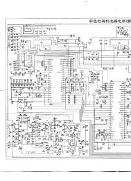
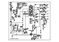
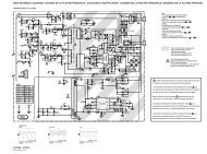
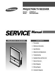
Schematic DiagramsFor schematic Diagram- Resistors are in ohms, 1/8W unless otherwise noted.- Circled numbers refer to waveforms.NoteSpecial note :Most semiconductor <strong>de</strong>vices are electrostatically sensitive and therefore require the special handling techniques<strong>de</strong>scribed un<strong>de</strong>r the “electrostatically sensitive (ES) <strong>de</strong>vices” section of this service manual.Note :Do not use the part number shown on this drawing for or<strong>de</strong>ring. The correct part number is shown in the partslist (may be slightly different or amen<strong>de</strong>d since this drawing was prepared).Important safety notices :Components i<strong>de</strong>ntified with the mark have the special characteristics for safety. When replacing any of thesecomponents. Use only the same type.3 Block I<strong>de</strong>ntification of Main PCB(OPTION)(OPTION)(Component Si<strong>de</strong>)(Conductor Si<strong>de</strong>)11-2 Samsung Electronics