Very Sharp Platinum Tips by Electrochemical Etching
Very Sharp Platinum Tips by Electrochemical Etching
Very Sharp Platinum Tips by Electrochemical Etching

Create successful ePaper yourself
Turn your PDF publications into a flip-book with our unique Google optimized e-Paper software.
Martin Kupper<strong>Very</strong> <strong>Sharp</strong> <strong>Platinum</strong> <strong>Tips</strong> <strong>by</strong><strong>Electrochemical</strong> <strong>Etching</strong>Bachelor ThesisFor obtaining the academic degreeBachelor of ScienceBachelor Program of Technical PhysicsGraz University of TechnologySupervisor:Univ.-Prof. Ph.D. Peter HadleyInstitute of Solid State PhysicsGraz, May 6, 2012
<strong>Very</strong> sharp platinum tips Martin Kupper 0830965Contents1 Introduction 32 State of the art 42.1 <strong>Electrochemical</strong> etching . . . . . . . . . . . . . . . . . . . . . . . . . . . 42.2 <strong>Tips</strong> for resistivity measurements. . . . . . . . . . . . . . . . . . . . . . 53 Experimental methods 73.1 Spot welding . . . . . . . . . . . . . . . . . . . . . . . . . . . . . . . . 73.2 <strong>Etching</strong> . . . . . . . . . . . . . . . . . . . . . . . . . . . . . . . . . . . 73.3 Annealing . . . . . . . . . . . . . . . . . . . . . . . . . . . . . . . . . . 93.4 Micropolishing . . . . . . . . . . . . . . . . . . . . . . . . . . . . . . . 113.5 Removing the oxide - ”reverse polishing” . . . . . . . . . . . . . . . . . 134 Tip properties 154.1 Elastic properties . . . . . . . . . . . . . . . . . . . . . . . . . . . . . . 154.2 Electrical properties . . . . . . . . . . . . . . . . . . . . . . . . . . . . 172
<strong>Very</strong> sharp platinum tips Martin Kupper 08309651 IntroductionThe tips used up to now to make electrical measurements in an SEM at the SEMlaboratory of the Institute of Solid State Physics [1], are industrially manufacturedtungsten tips (see Fig.1.1). To make electrical contact, the tip has to be pressed veryhard on the surface of the sample and because the tip is very sharp (about 500 nm)it bends. So the contact between the tip and the sample is not at the head of the tip,but somewhere behind. It is also not possible to say how big the contacting part ofthe tip is. So the aim of this project was to try and make very sharp Pt/Ir tips, testtheir elastic and electrical properties and test if these tips are more suitable for theelectrical measurements which are currently done at the SEM laboratory. The projectis based upon the paper <strong>Very</strong> sharp platinum tips for scanning tunneling microscopy[2].The produced tips have a sharp shape and are about 60 - 150 nm thick at theend. (See Figs.3.8 and 3.10) They also have good electrical properties, if the oxidelayer is being removed. It there is an oxide layer, however, there is then a problemin making contact with the sample. During the project it was not possible to makegood contact between a Pt/It tip and the silicon samples which were analyzed at thetime, but there was good contact between the tips. The resistivity was about 30 - 50 Ω.The elastic properties were not as bad as expected, but nor were they as good ashoped. After crashing on the surface the tip went back a bit, but it was bent (seeFig.3.7).Figure 1.1: An etched Pt/Ir tip (left picture), compared with an industrially manufacturedtungsten tip (right picture)3
<strong>Very</strong> sharp platinum tips Martin Kupper 08309652 State of the art2.1 <strong>Electrochemical</strong> etchingThe electrochemical etching of very sharp tips is an established procedure for scanningtunneling microscopy [5]. It is possible to make tips out of different metals, butbasically the process is the same every time. A wire is dipped in an electrolyte, anda voltage is applied between the wire and a counter electrode [11]. The voltage - andwhether it is AC or DC - depends on the metal and electrolyte used and has to bedetermined <strong>by</strong> experiment. Then the oxide layer, whitch appears during the etching,has to be removed <strong>by</strong> another electrochemical step. This is usually done with a small,negative DC voltage, where the tip is the ground. It is possible to do a further stepbetween the etching and the oxide removal, called micropolishing. This is actually asecond etching with an other electrolyte or an acid, and usually a lower voltage. Thisation of cobalt and nickel 2565reduces the diameter of the head of the tip again and produces a smooth surface [2].3560 I. H. Musselman and P. E. Russell: <strong>Platinum</strong>liridium tips(a) A nickel tip etched with a (b) A Pt/Ir tip etched with CaCl 2 /H 2 O/HCl.KCl solution. [6][12]FIG. 4. SEM images of Ni tips a lower tip; b upper tip; Magnifications:FIG. 5. SEM images of the same Ptllr tip shown in Fig. 3 after micropolishing.a Radius 11000, of curvature b < SOO 300, A. Cone b half angle 800, of 8". b 3000.a 200, a 2000,Figure 2.1: Different kinds of tips.The current I flowingtips, however,duringPt peaksthewereetchingnot observedprocesssuggesting thatis shown inthe surface C layer was in excess of the escape depth ofthe PtFig. 2.Auger electron.The relative thicknesses of the surface contamination layerscan for the becut identified versus the etched inPt/Ir thetips electrochemical were determined etch-Two regimes<strong>by</strong> monitoring the intensity of the C Auger signal as a functionof sputtering time (3 keY, 25 mA emission current,ing of Me: Point 1→2 and Point 2→3. This behavior is dueto a decreased 4 charge X 10 - 5 Pa Ar). carriers For the cut concentration, tip, the C signal reached backgroundafter 45 s of sputtering, whereas the sputtering timeas a consequenceof the precipitation varied from 30 s to 3 of min the for the Me three etched complexes. Pt/lr tips. Thislarge variation in C thickness among the etched tips wasWhen the electrochemical reflected in their STM imaging etching unpredictability. starts Out Point of 20 1, hydratedchemicaletched species4Pt/Ir tips,formsapproximatelyaround20% (thosethepresumablywire, spreadingwith minimal surface C) successfully imaged sputter-deposflame.Unfortunatelyat least 30 min per tiflame temperature, iC without altering thzation. The extent oprecautions were takthe etching setup. Calevel observed for thminated from the etcreadily dissolves in wvapor pressure than<strong>by</strong> boiling and subsethe tips and to prepaing step, the contactthe thin film of etchabox under a N2 atmAuger survey speCO 2was removed frfavorably with that awerc observed for allA special method for etching tips on the is tip reverse surface etching composition. [3]. Carbon Here the was wire observed is not in all dipped offor the cut and etchein the etch solution from above, the but survey instead spectra.Anode: Mes +4Cl − from For underneath.the cut→ MeCl 2 tip, Pt peaks This4 +2e − were is carried also observeddefining the upper thickness of the carbon . contaminoutof the Pt Auger electAr + ion beam to spwith a layer of high-density electrically insulating liquid under the electrolyte. Theation layer to be between 20 and 50 A. For two of the etchedwhereas a range of 2wire is in this liquid and protudes a little in the electrolyte. This way the tips get anextremely slim shape (see Fig.2.2) [4]. However, because of the setup, doing this kindc. Image acquisitiof etching is a lot more complex then the etching from above.Two sets of nine Petching procedure wwere tested <strong>by</strong> imagspikes or streaks weusing tips from eithacquired using 80%pearance with rounhigh ranging from 1unusual features obsremaining 20% of thdesirable tip shape rface chemistry.
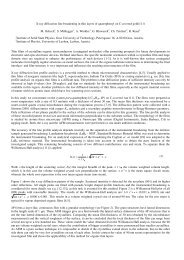
2 State of the art Martin Kupper 0830965rall profiles, <strong>by</strong> transmission electron microsification,of tungsten tips of decreasing conetwo-step etching. They display many minitipsat appears independent of their location alongwith water and alcohol for removregularlayer of electrolyte residue,ediately in an inert medium such asavoid oxidation or thin film depositsuntil actual use.true atomic or near-atomic sharpness,e were imaged with a high-resolutionmicroscope model Hitachi H-800NAand optimized for 0.26 nm point-to-ic profiles of tips sharpened <strong>by</strong> reprogressivelydecreasing cone anglesat low magnification. They illustratel ultrasharp minitips or spikes alongabsence of correlation between coned spike sharpness. The removal of therinsing in water and alcohol does notpness, as displayed <strong>by</strong> the very sharpic radius OS-l.0 nm and half-cone. To put in perspective the tip profilepness yielded <strong>by</strong> reverse etching andmbody in comparison with typical tipnormal etching, a clean minitip ofs (subnanometer radius) is shown inat the same magnification, on thesharp tungsten minitips of near-atomic radiushalf-cone (y-14’) unaltered <strong>by</strong> rinsing withFIG. 5. Tip of near-atomic sharpness of apex radius about 0.5-1.0 nm,formed Figure <strong>by</strong> reverse 2.2: ac Aetching reverse-etched (inside), contrasted tungsten at the same tip. magnitica- [3]tion with the outlined profile of a typically sharp apex of lOO-nm radiusformed <strong>by</strong> normal ac etching (outside).2.2 <strong>Tips</strong> for resistivity measurements.outlined profile of an optimal tip of about 100 nm radiusproduced <strong>by</strong> standard etching.In summary, a new procedure has been developed forthe production <strong>by</strong> electrochemical etching of ultrasharptungsten tips of nanometer and subnanometer apex dimensionsand its mechanism based on bubble dynamics brieflydiscussed. <strong>Tips</strong> are etched in NaOH under ac voltage intwo slow steps: In the first, a narrow cone with a fairlyblunt tip is produced, and in the second, the final sharpeningis accomplished in a modified configuration in whichthe wire is immersed pointing upward.The procedure can be extended to other metals withappropriate electrolytes.More broadly, beyond scanning probe microscopy, ultrasharptips also have applications in nanolithography,low-voltage cold-cathode field emitters, nanoelectronics,electrochemistry, field-ion and electron microscopy, andcell biology.The author is greatly indebted to Professor Noel A.Clark for use of the STM and etching setup in the CondensedMatter Laboratory and to Professor Arnold0 Majerfeldand Dr. Tamsin McCormick for use of the HitachiH-800NA transmission electron microscope in the AtomicResolution STEM Laboratory on the Boulder Campus.<strong>Sharp</strong> tips are also used for resistivity measurements in an SEM [1], where the currentdistribution of small devices is being measured. To do that, sharp tips are mountedin micromanipulators, are installed in an SEM. The tips are placed on the device, tomake electrical contact, a voltage is applied and the drop measured. In general, thereare two ways to make these measurements: first the normal resistivity measurementwith two tips, and secondly the four point resistivity measurement. For the four pointmeasurement the tips are placed in a row, a current applied between the two outer tipsand the voltage drop measured between the two inner tips (see Fig.2.3). In addition,the problem with this measurement is the tips. As mentioned in chapter 1 they bendwhen they are landed on a sample (see Fig.2.4). Because it can only be estimatedwhere the tips make contact, it is that way a relatively inaccurate measurement. Forfurther information concerning this method, visit the hompage of the Institute of SolidState Physics from the TU Graz [1].‘G. Binnig, H. Rohrer, Ch. Gerber, and E. Weibel, Phys. Rev. Lett. 49,57 (1982); 50, 120 (1983).‘G. Binnig, C. F. Quate, and Ch. Gerber, Phys. Rev. Lett. 56, 930(1986).‘J. Tersoff and D. R. Hamann, Phys. Rev. Lett. 50, 1998 (1983); Phys.Rev. B 31, 805 (1985).4T. E. Feuchtwang, P. H. Cutler, and N. M. Miskovsky, Phys. Lett. A99, 167 (1983).‘N. D. Lang, Phys. Rev. Lett. 55, 230 (1985); 56, 1164 (1986).bJ. K. Gimzewski, A. Humbert, J. G. Bednorz, and B. Reihl, Phys. Rev.Lett. 55, 951 (1985).‘Y. Kuk and P. J. Silverman, Appl. Phys. Lett. 48, 1597 (1986).‘R. Chicon, M. Ortuno, and J. Abellan, Surf. Sci. 181, 107 (1987).‘P. K. Hansma and J. Tersoff, J. Appl. Phys. 61, Rl (1987).“J. E. Demuth, U. Koehler, and R. J. Hamers, 5. Microsc. 152, 299(1988).*lY. Kuk and P. J. Silverman, Rev. Sci. Instrum. 60, 165 (1989).“L. L. Soethout, H. van Kempen, and G. F. A. van de Walle, Adv..Electron. El. Phys. 79, 155 (1990).13A. J. Mehned, J. Vat. Sci. Technol. B 9, 601 (1991).14M. Fotino, Proc. Annu. Meet. EMSA 49, 386 ( 1991).Figure 2.3: Diagram of a four point measurement [1].tt., Vol. 60, No. 23, 8 June 1992 M. Fotino 2937ded 12 Jan 2012 to 129.27.158.207. Redistribution subject to AIP license or copyright; see http://apl.aip.org/about/rights_and_permissions5
2 State of the art Martin Kupper 0830965Figure 2.4: Four point measurement with four Pt/Ir tips produced during the project.One kind of measurement avoiding the bending problem is the spreading resistanceprofiling, in short ”‘SRP”’. The sample is ground diagonally and two tips with aconstant distance are pressed rectangular to the surface on the sample with one millionpounds per sq inch [7], so that they mechanically deform the sample surface (seeFig.2.5). But the SRP is only good for making measurements of carrier concentrationin semiconductors like silicon or germanium, so for making measurements on withsharp tips, the resistivity measurement has to be used.Figure 2.5: Illustration of the spreading resistance profiling [7].6
<strong>Very</strong> sharp platinum tips Martin Kupper 08309653 Experimental methods3.1 Spot weldingA short piece of 100 µm thick Pt/Ir wire was spot welded at the end of a tungstenwire. The tungsten wires used were 0.5 mm in diameter and between 2 and 4 cm long.The welding was done at two spots (Fig. 3.1) to make sure that the Pt/Ir wire wasfixed on the tungsten and that there was good electrical contact. The wire was cut sothat a 2 to 3 mm long piece was left over for the etching step.Figure 3.1: A finished tip.3.2 <strong>Etching</strong>The electrochemical etching was done with a CaCl 2 /H 2 O/acetone solution [2], namely20 ml distilled water with 20 ml acetone and 7g calcium chloride dihydrate. The solutionwas over-saturated with acetone, in order to create a thin film of acetone swimmingon the top of the solution. Using a syringe to put the solution from the storage bottleinto the the box where the etching was done, ensures that there will not be an acetonefilm which could influence the process.For the etching, the Pt/Ir wire should be dipped in the solution about 1 mm deep.It is not important that the wire is dipped in perpendicular to the fluid surface. Agraphite rods was used as the counter electrode [8](Fig. 3.2). Experiments with copper7
3 Experimental methods Martin Kupper 0830965Figure 3.2: The graphite electrode (the big one) and the pencil lead (the small one).Figure 3.3: The setup for the etching. Bubbles can be seen appearing as a white shapearound the tip.and steel as the counter electrode did not yield the desired results. Using these metals,an oxide layer appeared and because of the change of the resistance these etchings werenot successful. <strong>Etching</strong> with the lead of an ordinary pencil as the counter electrodeproduced almost the same results as with the graphite rod, because pencil leads aremade of graphite mixed with clay [9] (see Fig. 3.2). Although the graphite does notreact with the CaCl 2 /H 2 O/acetone solution, the electrode has to be cleaned after 10 -20 etchings. Usually it is sufficient to flush it with distilled water. During the etchingprocess PtCl is formed. That is a black precipitate which adheres to the graphite.The influence of PtCl depostits on the resistivity of the graphite was not measured,but when the graphite electrode, after 20 etchings, was put in a fresh solution, a blackcloud appeared around the electrode.For the electrochemical etching a sinusoidal voltage was applied between -20 and 20V at 40 Hz [2]. The etching had to be stopped when the current intensity fell below20 mA. For our setup, a Keithley Source Meter 2636 A was used as the voltage source.The program used for the etching can be found in Appendix A4.2.During the etching bubbles can bee seen appearing around the Pt/It wire. Becauseof the acetone in the solution, they stay very small (around 0.1 mm) [2]. But afteretching a few tips the solution becomes more viscous and there<strong>by</strong> the bubbles biggerand more stable. It turned out that when the viscosity of the solution exceeds a certainvalue, the bubbles became so big and stable, that the contact between the tip and the8
3 Experimental methods Martin Kupper 0830965Figure 3.4: A well etched tip compared to a tip etched with an over-usedCaCl 2 /H 2 O/acetone solution.solution is no longer the surface of the solution, but rather the membrane of one ormore bubbles. That means that the contact is higher than the solution surface andthere<strong>by</strong> the sharp part of the tip is etched away. Such a tip is shown in Fig. 3.4. Howmany tips can be etched before changing the solution depends on how deep the Pt/Irwire is dipped into the solution, so on how much material is etched away. For etching4 tips which were dipped in the wire about 1 mm, a solution of 17 - 20 ml was used.It wasn’t possible to make more than 5 tips without changing the solution.After etching, the tips should be cleaned with distilled water. They should be dippedin a bowl filled with water, and moved left and right a little bit. If done carefully, theycan be flushed, if the water is allowed to flow too quickly while flushing, the tips caneasily be bent.After the etching step the tips are usually around 200 nm thick with a slim shape(seeFig. 3.5).3.3 AnnealingThe annealing is carried out for two reasons. Firstly, the surface of the tip after theetching is not very smooth (see Fig. 3.5). But more importantly, the heating of the tipreduces the amount of dislocations in the Pt/Ir, and there<strong>by</strong> the grains in the materialget bigger [2]. Thus the elastic properties of the tip are changing. An unannealed tipjust bends if it is pressed on a surface. This will be discussed in section 4.1.The annealing was done with a bunsen-burner, the wire was heated to red-heat for10 - 20 s. This step slightly enlarged the diameter of the tip (see Fig. 3.6).Test of the elastic properties were tested <strong>by</strong> bending one tip at the right edge of thesilicon sample which was in the SEM at this time (see Fig. 3.7). The elastic propertieswere not as bad as expected. The tip was deformed, but after taking the tip awayfrom the silicon it bent back to a certain value.9
3 Experimental methods Martin Kupper 0830965Figure 3.5: Two tips after the etching step. The right picture shows the same tip asthe left with higher magnification.Figure 3.6: Two tips before and after the annealing step. The pictures on the rightshow the same tips as on the left but with higher magnificationThe tips should be cleaned again after the annealing as with the etching (Section3.2).10
3 Experimental methods Martin Kupper 0830965Figure 3.7: Test of the elastic properties of an annealed tip. The upper left pictureshows the tip before the bending. The three pictures on the right show twocareful crashes, and the two lower on the left a brutal crash on the silicon.3.4 MicropolishingTo reduce the diameter of the tip after the annealing and keep the surface smooth,an electrochemical micropolishing was done [2]. See Fig. 3.8 for the result. The microwirewas etched with an H 2 SO 4 solution diluted to 1% with distilled water. A goldwire-loop, with 4 mm in diameter, was dipped into the solution so that a thin filmappeared. The gold wire was mounted in a micromanipulator and under a opticalmicroscope it was moved so that the microwire was in contact with the H 2 SO 4 film(see Fig. 3.9). Because of the capillary action [10] the film coated the whole microwire.For the micropolishing a 3 V square wave voltage at 1kHz was applied for 12 s. Theelectrodes were the tip and the gold wire. During the micropolishing it was possible tosee bubbles appearing around the microwire, sometimes even without the microscope.It turned out, that this is not an indicator of the quality of the reaction if the bubblesare big. Sometimes it is an indication for that the contact between the H 2 SO 4 film11
3 Experimental methods Martin Kupper 0830965Figure 3.8: Two tips before (left) and after (right) the micropolishing.and the tip is not at the microwire, but at the ”thicker” part, where more materialis etched away. That might mean that the microwire loses contact with the film andprotrudes on the other side. This can be seen using a microscope and focusing onthe tip. There is no problem when moving the gold-loop back and forth a bit duringthe micropolishing to make sure that the microwire is being polished completely, or topolish some of the ”thick” part to make grain boundary visible (Fig. 4.2) - this willbe discussed in section 4.1.There is a problem, however, with the lifespan of the H 2 SO 4 film. If there is only agold loop it does not last long enough to finish the polishing. To have a longer lifespan,the loop has to be at the end of a twisted part (ours was 1.5 cm long - see Fig. 3.9),and the wire has to be tilted, so that the loop is below. The wire has to be dippedinto the H 2 SO 4 solution completely, so that there is enough solution available at thetwisted part to keep the film existing. This way the lifespan is about 1 - 2 min.It is not necessary to clean the tips after the polishing if the next step is done immediatelyafterwords. If there is a break in between which is long enough for the tipsto dry, it’s better to clean them afterwords, as with the etching (Section 3.2) and theannealing (Section 3.3).12
3 Experimental methods Martin Kupper 0830965Figure 3.9: The setup for the micropolishing. The gold wire with the H 2 SO 4 film canbe seen; when the picture was taken there was no contact between the filmand the microwire.3.5 Removing the oxide - ”reverse polishing”The micropolishing causes oxidation of the platinum [2]. The oxide layer preventselectrical contact with the tip, so it has to be removed. To do that, the tip hast to beput in the same setup as in the micropolishing step, and a -1.1 DC voltage applied for2 min [2]. The ground has to be at the gold wire. During the process bubbles appearagain, but a lot smaller than during the micropolishing. Here they can be seen onlythrough the microscope and they slowly decrease with time. But when the oxide layeris removed, etching of the platinum should be continued slowly so that the occurrenceof bubbles does not stop after the oxide is gone. After 2 min reverse polishing therewas good electrical contact between all tips. The tips also became a little sharper afterremoving the oxide layer (Fig. 3.10).Because this is the last step, the tips had to be cleaned afterwords with distilledwater, as with the annealing and the etcing (see section 3.2).13
3 Experimental methods Martin Kupper 0830965Figure 3.10: Two tips before (left) and after (right) the removal of the oxide layer.14
<strong>Very</strong> sharp platinum tips Martin Kupper 08309654 Tip properties4.1 Elastic propertiesOne of the main intentions of the project was to produce flexible tips, so that afterpressing them on the sample surface they return back to their former shape. Thecrucial step for this property is the annealing. Before that the tips have very littleflexibility, they just bend (see Fig.4.1). After the annealing, the tips get some flexibility(Fig.3.7), but for making electrical measurements they have to be pressed so hardon the surface that they still get bent. So in this respect the same problem occured aswith the tungsten tips.Figure 4.1: Test of the elastic properties of an unannealed tip.The reason for the change of the properties is that the amount of dislocations in thePt/Ir is reduced during the annealing, so the micro-crystals (grains) get bigger. Thelonger the annealing is done the bigger the grains should be; however, this was not observedin great detail, so a relation between grain size and endurance of the annealingcannot be given. After the micropolishing of an annealed tip the grain boundaries arevisible (see Fig.4.2). They can be seen on one hand because of their different color,and on the other because they are separated <strong>by</strong> thin lines, as clearly shown on theright, upper picture in Fig.4.2. In the best case the micro-wire should be a singlemicro-crystal, it wasn’t possible for us to prove that, because the resolution of our15
4 Tip properties Martin Kupper 0830965Figure 4.2: Grain boundaries after the micropolishing. The upper right picture wastaken with the back scattering detector, the others with 5kV accelerationvoltage. On the lower pictures the same tip is shown; the picture on theright shows that there is a grain boundary at the point the micro-wirebegins.SEM was insufficient. In the right, lower picture a grain boundary can be seen at thepoint where the micro-wire begins. We expected to see smaller grains on micropolishedunannealed tips, but we did not (Fig.4.3).16
4 Tip properties Martin Kupper 0830965Figure 4.3: The surface of two micropolished, unannealed tips. It is not possible tolocate any grain boundaries on the surface.4.2 Electrical propertiesBecause the tips are to be used for electrical measurements, the electrical propertiesof the tips have been studied. The resistivity between two tips is about 30 - 50 Ω, ifthe oxide layer has been removed. If there is an oxide layer, there is a bigger chanceof melting the tip than breaking through the oxide. More important though is thecontact to the sample. It was impossible to create such a contact. Fig.4.4 showns twoEBIC measurements of two PT/It tips in contact with a silicon sample. It can be seenthat the contact between the tip and the sample is not at the head of the tip. ThreeIV curves are shown in Fig.4.5.Figure 4.4: EBIC measurement of two Pt/Ir tips on a silicon sample. A separateEBIC measurement was made for each tip. For an unknown reason bothtips could not be measured at the particular time. For the correspondingIV curves see Fig.4.5.17
4 Tip properties Martin Kupper 0830965We also tried to electroform the tips, in order to melt them onto the silicon sample.But the voltage source used was unable to produce a high-enough voltage. The highestvoltage applied was 200 V.Compared with the industrially manufactured tungsten tips, the electrical propertiesbetween two tips are more or less the same, but with tungsten tips better contactwith a sample can be made. That is because on the one hand tungsten is a a muchharder material than platinum, and on the other hand, the industrially manufacturedtungsten tips are thicker than our home-made Pt/It tips, so they are more stable. Wecould have tried to make contact with a comparable thick Pt/Ir tip, but that wouldnot have been reasonable, because we wanted to have sharper tips so that we wouldknow more precisely where the contact with the sample was made. With Pt/It tipsthe same size as the tungsten tips, there would also be the same problem. Probably itwould be even greater because Pt/It is not as hard as tungsten, and moreover, platinumis more expensive than tungsten. So one could try to make very sharp tungstenor even silicon tips [5].18
4 Tip properties Martin Kupper 08309650.50I/mA−0.5−1−1.5−2−20 −15 −10 −5 0 5 10 15 201 x 10−6 U/mV(a) 1 st IV0.50I/mA−0.5−1−1.5−2−30 −20 −10 0 10 20 301 x 10−4 U/mV(b) 2 nd IV42I/mA0−2−4−6−50 −40 −30 −20 −10 0 10 20 30 40 506 x 10−4 U/mV(c) 3 rd IVFigure 4.5: Three IV curves of two Pt/Ir tips. They were always at the same position.For the corresponding EBIC see Fig.4.419
<strong>Very</strong> sharp platinum tips Martin Kupper 0830965Bibliography[1] Institute of Solid State Physics, Graz University of Technology[Electrical Measurements in a SEM] [http://www.if.tugraz.at/][2] <strong>Very</strong> sharp platinum tips for scanning tunneling microscopy, L. Libioulle,Y.Houbion, J.-M. Gilles, Rev. Sci. Instr. vol.66 p.97 (1995)[3] Nanotips <strong>by</strong> reverse electrochemical etching, Mircea Fotino, Appl. Phys. Lett. 60 ,p. 2935 (1992)[4] Preparation of platinum/iridium scanning probe microscopy tips, A. H. Sørensen,U. Hvid, M. W. Mortensen, K. A. Mørch, Rev. Sci. Instrum., Vol. 70, No. 7, p.3059 (1999)[5] On the electrochemical etching of tips for scanning tunneling microscopy, J. P. Ibe,P. P. Bey, Jr., S. L. Brandow, R. A. Brizzolara, N. A. Burnham, D. P. Dilella, K.P. Lee, C. R. K. Marrian, R. J. Colton, J. Vac. Sci. Technol. A 8 p.3570 (1990)[6] <strong>Electrochemical</strong> fabrication of cobalt and nickel tips for scanning tunneling microscopy,C. Albonetti, M. Cavallini, M. Massi, J. F. Moulin, F. Biscarini, J. Vac.Sci. Technol. B 23(6), p. 2564 (2005)[7] Spreading Resistance Profiling, Wikipedia, the free encyclopedia [en.wikipedia.org- SRP][8] Technologie und Vertriebs GmbH Bayern [www.graphit-edm.de][9] Pencil, Wikipedia, the free encyclopedia [en.wikipedia.org - Pencil][10] Capillary action, Wikipedia, the free encyclopedia[en.wikipedia.org - Capillary action][11] The art and science and other aspects of making sharp tips, Allan J. Melmed, J.Vac. Sci. Technol. B 9 (2), Mar/Apr 1991[12] <strong>Platinum</strong>/iridium tips with controlled geometry for scanning tunneling microscopy,I. Holl Musselman, P. E. Russell, J. Vac. Sci. Technol. A 8 (4), p. 3558(1990)20
<strong>Very</strong> sharp platinum tips Martin Kupper 0830965Sine loop program for the etchingamp_v = 1000m_delay = 0.001list_v = {0.309, 0.588, 0.809, 0.951, 1, 0.951, 0.809, 0.588, 0.309,-0.309, -0.588, -0.809, -0.951, -1, -0.951, -0.809, -0.588, -0.309}-------------------config SMU A-------------------------smua.reset()smua.measure.autorangei = smua.AUTORANGE_ONsmua.source.func = smua.OUTPUT_DCVOLTSsmua.source.levelv = 0smua.source.limiti = 50e-3smua.measure.nplc = 0.001smua.nvbuffer1.clear()smua.nvbuffer1.appendmode = 1smua.nvbuffer1.collectsourcevalues = 1smua.nvbuffer2.clear()smua.nvbuffer2.appendmode = 1smua.nvbuffer2.collectsourcevalues = 1smua.measure.count = 1display.smua.measure.func = display.MEASURE_DCAMPS------------------measurement-----------------------smua.source.output = smua.OUTPUT_ONsmua.measure.delay = m_delayi = 1reading = 1repeatsmua.source.levelv = math.sin(i)*20delay(0.0008)i = i + 0.25if i > 360 theni = 1endif i == 90 thenreading = smua.measure.i()print(reading)enduntil reading < 0.02021