Differential Open Resonator Method for Permittivity Measurements ...
Differential Open Resonator Method for Permittivity Measurements ...
Differential Open Resonator Method for Permittivity Measurements ...

Create successful ePaper yourself
Turn your PDF publications into a flip-book with our unique Google optimized e-Paper software.
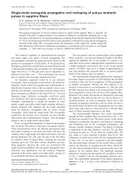
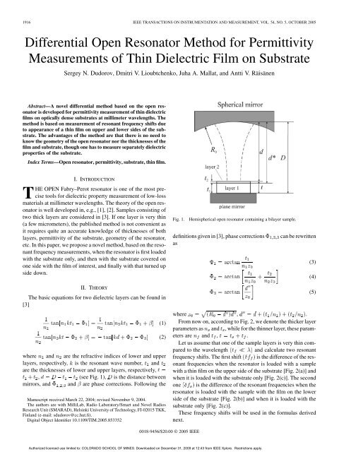
1916 IEEE TRANSACTIONS ON INSTRUMENTATION AND MEASUREMENT, VOL. 54, NO. 5, OCTOBER 2005<strong>Differential</strong> <strong>Open</strong> <strong>Resonator</strong> <strong>Method</strong> <strong>for</strong> <strong>Permittivity</strong><strong>Measurements</strong> of Thin Dielectric Film on SubstrateSergey N. Dudorov, Dmitri V. Lioubtchenko, Juha A. Mallat, and Antti V. RäisänenAbstract—A novel differential method based on the open resonatoris developed <strong>for</strong> permittivity measurement of thin dielectricfilms on optically dense substrates at millimeter wavelengths. Themethod is based on measurement of resonant frequency shifts dueto appearance of a thin film on upper and lower sides of the substrate.The advantages of the method are that there is no need toknow the geometry of the open resonator nor the thicknesses of thefilm and substrate, though one has to measure separately dielectricproperties of the substrate.Index Terms—<strong>Open</strong> resonator, permittivity, substrate, thin film.I. INTRODUCTIONTHE OPEN Fabry–Perot resonator is one of the most precisetools <strong>for</strong> dielectric property measurement of low-lossmaterials at millimeter wavelengths. The theory of the open resonatoris well developed in, e.g., [1], [2]. Samples consisting oftwo thick layers are considered in [3]. If one layer is very thin(a few micrometers), the published method is not convenient asit requires quite an accurate knowledge of thicknesses of bothlayers, permittivity of the substrate, geometry of the resonator,etc. In this paper, we propose a novel method, based on the resonantfrequency measurements, when the resonator is first loadedwith the substrate only, and then with the substrate covered onone side with the film of interest, and finally with that turned upside down.II. THEORYThe basic equations <strong>for</strong> two dielectric layers can be found in[3]where and are the refractive indices of lower and upperlayers, respectively, is the resonant wave number, andare the thicknesses of lower and upper layers, respectively,, (see Fig. 1), is the distance betweenmirrors, and and are phase corrections. Following theManuscript received March 22, 2004; revised November 9, 2004.The authors are with MilliLab, Radio Laboratory/Smart and Novel RadiosResearch Unit (SMARAD), Helsinki University of Technology, FI-02015 TKK,Finland (e-mail: sdudorov@cc.hut.fi).Digital Object Identifier 10.1109/TIM.2005.853352(1)(2)Fig. 1.Hemispherical open resonator containing a bilayer sample.definitions given in [3], phase correctionsascan be rewrittenwhere , .From now on, according to Fig. 2, we denote the thicker layerparameters as and , while <strong>for</strong> the thinner layer, these parametersare and , .Let us assume that one of the sample layers is very thin comparedto the wavelength and calculate two resonantfrequency shifts. The first shift is the difference of the resonantfrequencies when the resonator is loaded with a samplewith a thin film on the upper side of the substrate [Fig. 2(a)] andwhen it is loaded with the substrate only [Fig. 2(c)]. The secondone is the difference of the resonant frequencies when theresonator is loaded with the sample with the film on the lowerside of the substrate [Fig. 2(b)] and when it is loaded with thesubstrate only [Fig. 2(c)].These frequency shifts will be used in the <strong>for</strong>mulas derivednext.(3)(4)(5)0018-9456/$20.00 © 2005 IEEEAuthorized licensed use limited to: COLORADO SCHOOL OF MINES. Downloaded on December 31, 2009 at 12:43 from IEEE Xplore. Restrictions apply.
DUDOROV et al.: DIFFERENTIAL OPEN RESONATOR METHOD FOR PERMITTIVITY MEASUREMENTS 1917Fig. 2.Samples to be introduced into the resonator. (a) Film is introduced on the upper side. (b) Film is introduced on the lower side. (c) Substrate only.A. Lower Layer Is Thin ( , )In this case, (1) and (2) can be trans<strong>for</strong>med toor by introducing a function and perturbation andusing (13)(6)where, assuming that terms proportional to are small, we canrewrite relations (3), (4), and (5), using the first two terms of aTaylor expansion(7)(8)(9)(10)(15)where the left side equalized to zero corresponds to the case of0 (substrate only), while the right-hand side of (15) is aperturbation due to presence of a thin film.Let us assume that the relative resonant frequency shift due topresence of a thin film is very small (in order of 10 ), and perturbationdoes not vary considerably due to this. It meansthat the slope is very small compared to that of in theintersection point. Using the method of small perturbations, wecan find the change of the wave number needed to makeequal towhere , . From (6), we can findthatWe can rewrite (7) as(11)from which we can find(16)(17)(12)Phase corrections , and changes of due to presenceof a thin film [in order of , see (9) and (10)]can be neglected (error 2.5%) compared to the terms proportionalto. At the next step, we will utilize the Taylorexpansion, the fact that the derivative of the tangent function is, and also the equation <strong>for</strong> the resonatorcontaining a substrate only(13)However, if, care must be taken whenusing the Taylor expansion, but we can simplify the equationsas follows. With 1% accuracy,,if0.17 rad (corresponding to 37, which is 0.025mm <strong>for</strong> sapphire at 100 GHz). There<strong>for</strong>e, we can rewrite (12) aswhere is calculated from (11).As be<strong>for</strong>e, we introduce a function(18)and perturbationAfter manipulations, we obtain(14)(19)(20)Authorized licensed use limited to: COLORADO SCHOOL OF MINES. Downloaded on December 31, 2009 at 12:43 from IEEE Xplore. Restrictions apply.
1918 IEEE TRANSACTIONS ON INSTRUMENTATION AND MEASUREMENT, VOL. 54, NO. 5, OCTOBER 2005Thusmakes (19) valid. Alternatively(21)(22)The resonant wave number shift due to a film on the upperside can be estimated(29)Dividing one frequency difference derived from (29) by theother one given by (17), we obtain(30)B. Upper Layer Is Thin ( , )In this case, , , , , .Now we can writeSimilarly to (18), we can simplify (23) and (24)(23)(31)where , and .Thus, (24) becomes(24)Furthermore(32)where .The Taylor expansion and perturbation method give(25)Thus(33)(34)(35)or(36)(26)(37)This can be simplified(27)Here, we have neglected the influence of changes in phasecorrections, as they are small compared to the terms proportionalto .Subtracting (22) from (37), and using the measured differencein the resonant frequencies of the resonator containing thesample with the film on the lower side and on the upper side, wecan calculate the difference in permittivities from the equationIntroducing a function and perturbation , we write(28)(38)where. Note, that if the permittivity of the filmis higher thanthat of thesubstrate, the resonantfrequency is lowerwhen the film is on the upper side of the substrate. Thus, we canmeasure the difference between permittivities of the film and thesubstrate. However, these measurements are difficult to carry outAuthorized licensed use limited to: COLORADO SCHOOL OF MINES. Downloaded on December 31, 2009 at 12:43 from IEEE Xplore. Restrictions apply.
DUDOROV et al.: DIFFERENTIAL OPEN RESONATOR METHOD FOR PERMITTIVITY MEASUREMENTS 1919TABLE IRESONANT FREQUENCY SHIFTS FOR 0.5-mm GaAs SUBSTRATE (0.63) WITHSAPPHIRE THIN LAYERS AND DIFFERENCE FROM (n 01)=(n 01) = 0.6940TABLE IIIEXPERIMENTAL RESULTS OF 6-m PHOTORESIST FILM ON 0.33-mmSAPPHIRE SUBSTRATETABLE IIRESONANT FREQUENCY SHIFTS FOR 0.6-mm GaAs SUBSTRATES (VERY CLOSETO 3=4) WITH THIN SAPPHIRE LAYERS AND DIFFERENCE FROM(n 0 1)=(n 0 1) = 0.6940TABLE IVEXPERIMENTAL RESULTS OF 6-m PHOTORESIST FILM ON0.50-mm GaAs SUBSTRATEaccurately,becauseofdecreasingofqualityfactoroftheresonatorcontaining such samples, even if the sample is lossless [5].Alternatively, we can divide (22) to (37), and using the measureddifference in the resonant frequencies of the resonatorcontaining the sample with the film on the lower side and onthe upper side, we can calculate the difference in permittivitiesfrom the equation(39)Equation (39) is more preferable, as the knowledge of the filmthickness is unnecessary.III. SIMULATIONDeveloped differential method was compared with themethod reported in [3] [(1) and (2)]. The behavior of the resonantfrequency of a hemispherical open resonator containing asample was simulated numerically. The 143.1651-mm distancebetween mirrors and the 149.4548-mm curvature radiuswere obtained using the calibration procedure describedin [5]. The refractive indices of GaAs and sapphire are takento be 3.59 and 3.06, respectively, giving a predefined value0.6940. We compared this value with thecalculated value of .The simulation results of the thin sapphire layers onthe 0.5-mm and 0.6-mm GaAs substrates at frequencies of105 GHz are presented in Tables I and II, respectively.Much larger frequency shifts are obtained <strong>for</strong> a thicker(0.6-mm) GaAs substrates (see Table II). It can be explainedby the fact that the upper surface of the sample comes closer toa maximum of the electric field, and there<strong>for</strong>e, the sensitivityto the thin layer becomes higher. It is possible to detect andmeasure even a micrometer-thick film in that case. However,it becomes more difficult to find the resonant peaks due to theincrease of the plane mirror absorption [5].IV. EXPERIMENTTwo 6- m AZ4562 photoresist films were deposited onto0.33-mm sapphire and 0.50-mm GaAs substrates. <strong>Measurements</strong>were per<strong>for</strong>med at different frequencies with the openresonator (Fig. 1) and an AB Millimetre 5–350-GHz VectorNetwork Analyzer connected to it.Prior to the measurement, the resonant frequencies of six0.53-mm sapphire substrates were compared at frequenciesclose to 80.3 GHz in the resonator in order to find two ofthem with the closest resonant frequencies. On one of them, a6- m photoresist film was deposited, while the second waferwas a “reference sample.” Three resonant frequencies of theresonator, loaded with the “reference sample,” the substratewith the film on the upper side, and the substrate with the filmon the lower side were measured.The preliminarily measured difference of the resonant frequencies<strong>for</strong> the “reference sample” and the substrate only wastaken into account. After that the resonant frequency shifts andthe relations between them were calculated. The permittivity ofthe film was calculated using (39). The procedure of the resonantfrequency measurement was repeated 5–7 times, and theresults were averaged. Tables III presents the measurement resultsand the calculated permittivities of the photoresist film onthe sapphire substrate.<strong>Measurements</strong> were repeated <strong>for</strong> the GaAs substrate with thesame photoresist film (Table IV).V. DISCUSSIONThe developed differential method allows to estimate the permittivityof the film on the substrate with accuracy within 5%and 2% <strong>for</strong> 0.6-mm and 0.5-mm substrate thickness, respectively,with film thickness up to 15 m. The above uncertainty iscaused at least by the following applied approximations: Taylorexpansion, were assumed to be constant, perturbationapproach, etc. In the case of thicker films, the accuracy becomesworse due to approximations used in the derivation of(39). Meanwhile, (39) gives a better accuracy <strong>for</strong> substrates withthicknesses approaching ,due to larger frequency shifts to be measured.The theory cannot be used if the substrate thickness is aboutbecause of tangential function used in the approximationbecomes zero. On the other hand, if, the quality factor of the resonant peak dramatically decreases.There<strong>for</strong>e, the desired discrete substrate thicknesses areabout , .The main contribution to errors comes from the experiment.This is because of the nonideality of the open resonator (roughnessand nonideal flatness of the plane mirror), environmentalAuthorized licensed use limited to: COLORADO SCHOOL OF MINES. Downloaded on December 31, 2009 at 12:43 from IEEE Xplore. Restrictions apply.
1920 IEEE TRANSACTIONS ON INSTRUMENTATION AND MEASUREMENT, VOL. 54, NO. 5, OCTOBER 2005instabilities (temperature, humidity), nonideal flatness of the investigatedsamples, etc. These result in about 10%–15% uncertaintyin obtained film permittivities.VI. CONCLUSIONHemispherical open resonator technique is developed <strong>for</strong>measurements of permittivity of thin films on optically densesubstrates. The method is based on measurement of resonantfrequency shifts due to appearance of the thin film on the upperand lower side of the substrate. The main advantage of thisdifferential method is that if the permittivity of the substrateis known, it is unnecessary to know the dimensions of theresonator and thicknesses of the substrate and film.<strong>Measurements</strong> of photoresist films on the 0.5-mm GaAs and0.33-mm sapphire substrates were carried out. Obtained resultsshow the method can be successfully employed <strong>for</strong> measurementof dielectric constant of thin films on a substrate.ACKNOWLEDGMENTThe authors would like to thank Prof. V. Lyubchenko fromthe Institute of Radioengineering and Electronics, RussianAcademy of Science, <strong>for</strong> fruitful discussions and providingsamples. They would also like to thank Dr. V. Ovchinnikovfrom the Microelectronics Center of TKK <strong>for</strong> the help in thefilm deposition.REFERENCES[1] A. L. Cullen and P. K. Yu, “The accurate measurement of permittivityby means of an open resonator,” in Proc. Royal Soc. London, vol. A325,1971, pp. 493–509.[2] , “<strong>Measurements</strong> of permittivity by means of an open resonator. I.Theoretical,” in Proc. Royal Soc. London, vol. A380, 1982, pp. 49–71.[3] S. Wang, L. Hu, and D. Xu, “<strong>Open</strong> resonator technique <strong>for</strong> measuringmultilayer dielectrics,” Microw. Opt. Technol. Lett., vol. 16, no. 6, pp.368–371, 1997.[4] B. Komiyama, M. Kiyokawa, and T. Matsui, “<strong>Open</strong> resonator <strong>for</strong> precisiondielectric measurements in the 100 GHz band,” IEEE Trans. Microw.Theory Tech., vol. 39, no. 10, pp. 1792–1796, 1991.[5] T. Hirvonen, P. Vainikainen, A. Lozowski, and A. V. Räisänen, “Measurementof dielectrics at 100 GHz with an open resonator connectedto a network analyzer,” IEEE Trans. Instrum. Meas., vol. 45, no. 4, pp.780–786, Aug. 1996.Sergey N. Dudorov was born in the Kirov region,Russia, in May 1975. He received the M.Sc. degreein applied physics and mathematics from theDepartment of Radio Engineering and Cybernetics,Moscow Institute of Physics and Technology,Moscow, Russia, in June 1998. The topic was“Investigation of dielectric waveguides and devicesbased on them.” He received the Licentiate degreein June 2001 and the degree of Doctor of Science inTechnology in June 2002 at the Radio EngineeringLaboratory, Helsinki University of Technology(TKK), Espoo, Finland, in June 2001 and June 2002, respectively. He receivedthe Candidate of Science degree from the Moscow Institute of Physics andTechnology. The thesis title is “Rectangular dielectric waveguide and itsoptimal transition to a metal waveguide.”In November 1998, he joined the Radio Engineering Laboratory of TKK,where he is currently a Postdoctoral Researcher. His research activities are focusedon the dielectric property measurements in application to development ofnew devices <strong>for</strong> millimeter and microwave applications based on the dielectricwaveguides.Dmitri V. Lioubtchenko was born in Gorky, Russia,in May 1971. He received the B.Sc., M.Sc., andPh.D. degrees in applied physics and mathematicsfrom the Department of Physical and QuantumElectronics, Moscow Institute of Physics and Technology,Moscow, Russia, in 1993, 1994, and 1998,respectively.From 1994 to 1997, he was a Researcher in theInstitute of Radio Engineering and Electronics, RussianAcademy of Sciences, Moscow. From 1997 to1998, he was a Visiting Researcher at The Universityof Liverpool, Liverpool, U.K. In 1998, he joined the Radio Laboratory ofHelsinki University of Technology, Espoo, Finland, where he is currently a PostdoctoralResearcher. His research interests and experience cover various topicsincluding investigations of new materials <strong>for</strong> millimeter, microwave, and optoelectronicapplications, particularly on the development of active and passivedielectric waveguides <strong>for</strong> the frequency above 100 GHz.Juha A. Mallat was born in Lahti, Finland, in1962. He received the Diploma Engineer (M.Sc.)with honors, Lic.Tech., and Dr.Tech. degrees inelectrical engineering from the Helsinki Universityof Technology (TKK), Espoo, Finland, in 1986,1988, and 1995, respectively.He has been with the TKK Radio EngineeringLaboratory (and its Millimeter Wave Group) since1985, working as a Research Assistant, SeniorTeaching Assistant, and Research Associate until1994. From 1995 to 1996, he was a Project Managerand Coordinator in an education project between TKK and the Turku Instituteof Technology. Since 1997, he has been a Senior Scientist with MilliLab(Millimetre Wave Laboratory of Finland—ESA External Laboratory), withthe exception of a period of one year during 2001–2002, when he served as aProfessor (pro tem) in Radio Engineering at TKK. His research interests andexperience cover various topics in radio engineering applications and measurements,especially in millimeter wave frequencies. He has also been involved inbuilding and testing millimeter wave receivers <strong>for</strong> space applications.Antti V. Räisänen received the Doctor of Science(Tech.) degree in electrical engineering from theHelsinki University of Technology (TKK), Espoo,Finland, in 1981.In the past, he has held Visiting Scientist positionsat the Five College Radio Astronomy Observatory(FCRAO) and the University of Massachusetts,Amherst, at Chalmers University of Technology,Gothenburg, Sweden, at the Department of Physics,University of Cali<strong>for</strong>nia, Berkeley, at the Jet PropulsionLaboratory and the Cali<strong>for</strong>nia Institute ofTechnology, Pasadena, and at the Paris Observatory and the University ofParis VI. Currently, he is a Chair Professor of Radio Engineering at TKK andis supervising research in millimeter wave components, antennas, receivers,microwave measurements, etc. at TKK Radio Laboratory, and leads theSmart and Novel Radios Research Unit (SMARAD). He serves also as theChairman of the Board of Directors of MilliLab (Millimeter Wave Laboratoryof Finland—ESA External Laboratory). He has authored and coauthored morethan 350 scientific or technical papers and six books, most recently RadioEngineering <strong>for</strong> Wireless Communication and Sensor Applications, MA:Artech House, 2003.Dr. Räisänen was the Chairman of the IEEE MTT/AP Chapter in Finlandfrom 1987 to 1992. He was the Secretary General of the 12th European MicrowaveConference in 1982, and served as the Conference Chair <strong>for</strong> the 22ndEuropean Microwave Conference in 1992, and <strong>for</strong> the 2nd ESA Workshop onMillimeter Wave Technology and Applications: Antennas, Circuits and Systemsin 1998, and as the Co-Chair <strong>for</strong> the 3rd ESA Workshop on Millimeter WaveTechnology and Applications: Circuits, Systems, and Measurement Techniquesin 2003. From 1995 to 97 he served in the Research Council <strong>for</strong> Natural Sciencesand Engineering, the Academy of Finland. In 1997, he was elected theVice-Rector of TKK <strong>for</strong> the period of 1997–2000. From 2002 to 2005, he servedas an Associate Editor of the IEEE TRANSACTIONS ON MICROWAVE THEORYAND TECHNIQUES.Authorized licensed use limited to: COLORADO SCHOOL OF MINES. Downloaded on December 31, 2009 at 12:43 from IEEE Xplore. Restrictions apply.