News Break - ULVAC Technologies
News Break - ULVAC Technologies
News Break - ULVAC Technologies

You also want an ePaper? Increase the reach of your titles
YUMPU automatically turns print PDFs into web optimized ePapers that Google loves.
JULY / AUGUST 2012<br />
Focus Topic...<br />
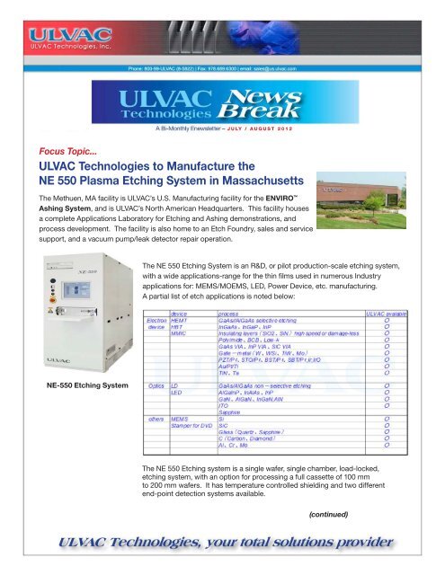
<strong>ULVAC</strong> <strong>Technologies</strong> to Manufacture the<br />
NE 550 Plasma Etching System in Massachusetts<br />
The Methuen, MA facility is <strong>ULVAC</strong>’s U.S. Manufacturing facility for the ENVIRO <br />
Ashing System, and is <strong>ULVAC</strong>’s North American Headquarters. This facility houses<br />
a complete Applications Laboratory for Etching and Ashing demonstrations, and<br />
process development. The facility is also home to an Etch Foundry, sales and service<br />
support, and a vacuum pump/leak detector repair operation.<br />
NE-550 Etching System<br />
The NE 550 Etching System is an R&D, or pilot production-scale etching system,<br />
with a wide applications-range for the thin films used in numerous Industry<br />
applications for: MEMS/MOEMS, LED, Power Device, etc. manufacturing.<br />
A partial list of etch applications is noted below:<br />
The NE 550 Etching system is a single wafer, single chamber, load-locked,<br />
etching system, with an option for processing a full cassette of 100 mm<br />
to 200 mm wafers. It has temperature controlled shielding and two different<br />
end-point detection systems available.<br />
(continued)
It corresponds to the substrate size to<br />
1100mm x 1400mm. The substrate can<br />
be Load /Unload by MGV.<br />
<strong>News</strong> <strong>News</strong><br />
<strong>Break</strong><br />
a-Si/µc-Si Tandem Solar Cell Manufacturing Process<br />
The NE 550 features the <strong>ULVAC</strong> proprietary Inductively Super Magnetron (ISM) plasma source, and the <strong>ULVAC</strong><br />
patented STAR Electrode (both depicted below). The ISM plasma source is a high density source that uses<br />
Substrate Substrate ID TCO Laser Insulation Substrate PE-CVD PE-CVD a-Si/µc-Si Laser PVD Metal Laser<br />
permanent Loading magnets. Cleaning The Marking STAR electrode Patterning enhances Tester process Cleaning repeatability System 1 System by 2keeping<br />
Patterning the quartz System(ICP)<br />
Patterning window<br />
clean and free from build-up of etch by-products.<br />
Laser Patterning Laser Patterning<br />
Laser Patterning<br />
TCO Glass Substrate TCO Laser Scribe a-Si Deposition µc-Si Deposition a-Si/µc-Si<br />
Laser Scribe<br />
Backside<br />
Electrode<br />
• 3D Profiler<br />
• 3D Profiler<br />
• Stylus Profiler<br />
• Ellipsometer<br />
• Resistance<br />
• Crystallization Rate<br />
• 3D Profiler<br />
• Stylus Profiler<br />
• Resistance<br />
a function that can evaluate optical characteristics in addition to the conventional measurement of deposition<br />
thickness, surface shapes, and resistance.<br />
The MPEC-1300 Multi-Probe Evaluation of Thin-Film Characterization System for tandem type solar cell<br />
has the following conventional measuring functions: (1) a “Surface Profiler,” which measures the deposition<br />
thickness and in-plane distributions of electrode-use thin films; (2) a “Low-resistance measurement,” which<br />
evaluates the resistance distributions of electrode-use metal thin films. In addition, four additional measuring<br />
functions have been intergraded including;<br />
(3) a “Raman Spectroscopy,” which maps in-plane distributions by<br />
obtaining µc-Si Crystallinity; (4) a “Three-dimensional (3D) measurement,” which three-dimensionally evaluates<br />
the shapes both of film surfaces after laser scribing and of TCO (Transparent Conductive Oxide) film surfaces;<br />
(5) a “Spectroscopic Ellipsometer,” which evaluates the optical constants of a-Si thin films; and (6) a “Highresistance<br />
measurement,” which evaluates the high-resistance distributions of a-Si thin films. By including a<br />
total of six types of measuring functions, the MPEC-1300 Multi-Probe Evaluation of Thin-Film Characterization<br />
System for tandem type solar cell has enabled the thin-film characteristics evaluation of tandem type thin-film<br />
solar cells to be performed in one system. In addition, since all surface areas of a glass substrate up to the<br />
5.5th-generation size can be measured with the system, there is no need to destroy substrates for evaluation.<br />
These excellent features can greatly reduce initial introduction costs and running costs by about 1/2 compared<br />
to when introducing two or more individual dedicated-use measuring instruments.<br />
This evaluation system is designed such that the user can select the measuring functions to be included<br />
according to the user’s purpose. <strong>ULVAC</strong> is also developing a system for evaluating the distributions of TCO<br />
Haze and solar cell local conversion efficiency.<br />
The newly released MPEC-1300 tandem type thin-film solar cell hybrid thin-film characteristics evaluation<br />
The system NE 550 will Plasma be available Etching starting System from is now June a 24, domestically 2009. For further (USA) manufactured information, please product. contact us.<br />
For Further Information, Please Contact Us…<br />
Contact Us<br />
Metal Scribe<br />
• 3D Profiler<br />
• Stylus Profiler<br />
<strong>ULVAC</strong> <strong>Technologies</strong>, your total solutions provider