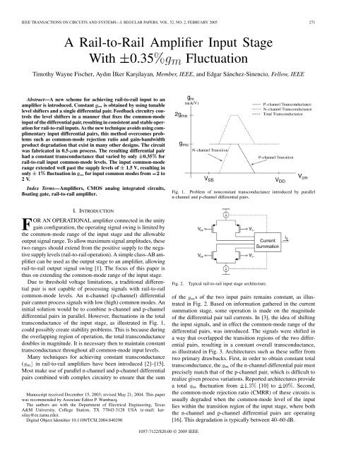
A Rail-to-Rail Amplifier Input Stage - Analog and Mixed Signal ...
A Rail-to-Rail Amplifier Input Stage - Analog and Mixed Signal ...
A Rail-to-Rail Amplifier Input Stage - Analog and Mixed Signal ...

Create successful ePaper yourself
Turn your PDF publications into a flip-book with our unique Google optimized e-Paper software.
272 IEEE TRANSACTIONS ON CIRCUITS AND SYSTEMS—I: REGULAR PAPERS, VOL. 52, NO. 2, FEBRUARY 2005Fig. 4.Programmable level shifting (PLS) circuitry.introduced by gate leakage via tunneling effects are sufficientlylarge, <strong>and</strong> are thus neglected in this analysis.Fig. 3. Obtaining constant transconductance by shifting the common-moderange of the input pairs <strong>to</strong> overlap transition regions.To overcome these problems, a technique that uses parallelsame channel differential pairs was introduced [15]. This techniqueis similar <strong>to</strong> [3] in that it shifts the common-mode rangeof one of the differential pairs. The primary difference is thatrather than overlapping transition regions <strong>to</strong> obtain constanttransconductance, the authors use feedforward cancellation <strong>to</strong>maintain constant when both of the input pairs are operating.Since only one type of differential pair is used, the matchingof the the two input transconduc<strong>to</strong>rs is much less sensitive <strong>to</strong>process variations. Still, the overall fluctuation in transconductanceof this circuit was nearly . Also, including thefeedforward transconduc<strong>to</strong>r, three differential pairs are used, aswell as some additional biasing circuitry, which increases thepower consumption of the amplifier.For simplicity <strong>and</strong> accuracy, it is best <strong>to</strong> use a single differentialpair at the input. In this case, the common-mode range of theinput pair must somehow be extended <strong>to</strong> accept rail-<strong>to</strong>-rail signals.In the past, this has been done using multiple input floatinggate transis<strong>to</strong>rs (MIFGs). The signal is attenuated using capacitivevoltage division before it is processed by the amplifier [1],[4]. The ratio of the MIFG capaci<strong>to</strong>rs is set so the input signalis attenuated enough <strong>to</strong> always reside within the common-moderange of the actual differential pair. To ensure the signal is sufficientlyattenuated, the capaci<strong>to</strong>r ratio in these architectures isusually set <strong>to</strong> around five, resulting in an attenuation of six [4].This adversely affects the gain-b<strong>and</strong>width product (GBW) aswell as the noise response of the amplifier. Furthermore, eventhese architectures that use a single input differential pair exhibitsome variance in the due <strong>to</strong> lambda effect on the tailcurrent. As the common mode rises or falls, so does of thetransis<strong>to</strong>r supplying the tail current, <strong>and</strong> accordingly, the current’smagnitude. Circuit simulations result in almost 3% deviationin across rail-<strong>to</strong>-rail common-mode inputs of a circuitimplemented in this way.In this paper, a new input stage for rail-<strong>to</strong>-rail operationis introduced, which makes use of a single input differentialpair. MIFG transis<strong>to</strong>rs are used, but feedback circuitryallows for a much lower attenuation than those previouslyreported. <strong>Rail</strong>-<strong>to</strong>-rail operation is achieved by shifting the inputcommon-mode level <strong>to</strong> a fixed dc level before the signal is input<strong>to</strong> the differential pair. It is assumed that any time constantsII. PROGRAMMABLE LEVEL SHIFTERSNear zero variance in can be achieved by shifting thecommon-mode component of the input signal <strong>to</strong> a fixed levelthat resides within the common-mode range of the input differentialpair. Since the amount of shift required is dependent on thecommon-mode level of the input, programmable level shifting(PLS) circuitry is needed. A simple, highly programmable levelshifter can be created with a MIFG transis<strong>to</strong>r in a source followerconfiguration, as displayed in Fig. 4. One terminal <strong>to</strong>the MIFG transis<strong>to</strong>r, , serves as the input <strong>to</strong> the circuit. Theother terminal, , determines the amount of shift by programmingthe effective threshold voltage of as seen from . Theamount of shift obtained from a transis<strong>to</strong>r in the source followerconfiguration is governed by the gate-<strong>to</strong>-source voltageFor, the resulting gate voltagein Fig. 4 of the MIFG transis<strong>to</strong>r with two inputs isCombining (1) <strong>and</strong> (2), the amount of shift from the point ofview of the input terminal is a recursive function of , determined<strong>to</strong> beDefining as the effective threshold voltage as seen from ,the amount of shift from <strong>to</strong> is nowwhere(1)(2)(3)(4)(5)(6)Since can be either a positive or negative value, canalso be programmed in either direction, with the amount of shif<strong>to</strong>btainable depending on the ratio of <strong>to</strong> .Nextwe
FISCHER et al.: RAIL-TO-RAIL AMPLIFIER INPUT STAGE 273Fig. 5.<strong>Rail</strong>-<strong>to</strong>-rail input stage.explore how <strong>to</strong> find a suitable value of <strong>to</strong> shift the commonmodelevel of differential signals <strong>to</strong> a constant value.III. FEEDBACK CIRCUITRYTwo programmable level shifters from the above sectionare now used as a pre-stage <strong>to</strong> a typical differential pair. Thecommon-mode level of the input signals is shifted <strong>to</strong> a constantvalue, yielding consistent operation independent of thecommon mode. In order <strong>to</strong> correctly program the level shifters,the common-mode information must be extracted from thecircuit, <strong>and</strong> fed back <strong>to</strong> the programming input, of Fig. 4.This is done using the architecture displayed in Fig. 5. Thesource voltage of the differential pair, labeled in Fig. 5 as ,behaves as an ac ground for differential inputs, <strong>and</strong> nearlyas a buffer for common-mode inputs. If this voltage remainsconstant, so will the magnitude of the tail current, resultingin near zero variation in of the differential pair. Any dcvalue that keeps the differential pair operating in the desiredsaturation region can be used as a reference. For convenience,the gate/drain voltage of , , is used for comparing .This difference is magnified <strong>and</strong> returned <strong>to</strong> the PLSs as .The resulting feedback voltage becomes:(7)stability analysis of the feedback loop is performed <strong>to</strong> ensureproper operation of the circuit.A. GBW <strong>and</strong> BiasingSince this design first attenuates the input signal before it isprocessed by the amplifier, the gain b<strong>and</strong>width product will bereduced. It is thus desirable <strong>to</strong> make this reduction as small aspossible. To achieve consistent rail-<strong>to</strong>-rail operation, the minimumattenuation can be obtained by setting in Fig. 5.There are two necessary conditions for using this attenuation.First, the feedback amplifier, , should have rail-<strong>to</strong>-rail outputsignal swing. Second, the conditionshould be met,where is the common-mode level of the input. This impliesthat the circuit should be designed such that when , is zero,should equal .The first requirement, that the feedback amplifier, has arail-<strong>to</strong>-rail output swing, is easily met by using an operationaltransconductance amplifier (OTA) based on three current mirrors[17]. The second requirement, thatcan be accomplishedthrough careful design of the circuit in Fig. 5, usingthe following relationships:(8)(9)Due <strong>to</strong> the negative feedback, if the gain of the amplifier is largeenough, is forced <strong>to</strong> be approximately equal <strong>to</strong> , <strong>and</strong> aconstant current is supplied <strong>to</strong> the differential pair regardless ofthe common mode. Also, since is equal <strong>to</strong> , the magnitudeof the tail current becomes precisely (neglecting devicemismatch) equal <strong>to</strong> the reference current.IV. DESIGN CONSIDERATIONSSeveral considerations need <strong>to</strong> be made in the design of thisamplifier. Two primary concerns in MIFG design are area <strong>and</strong>b<strong>and</strong>width. The addition of capaci<strong>to</strong>rs will increase the areaof the circuit compared <strong>to</strong> traditional amplifier design. Also,the attenuative effect of these capaci<strong>to</strong>rs reduces the effectivetransconductance of the input stage, degrading the GBW of theamplifier. One goal of this design should thus be <strong>to</strong> make theseeffects as small as possible. Proper biasing can help improve thecircuit performance, <strong>and</strong> minimize the required area. Finally, aSolving (2) <strong>and</strong> (8) yieldsCombining (7)–(12)(10)(11)(12)(13)
274 IEEE TRANSACTIONS ON CIRCUITS AND SYSTEMS—I: REGULAR PAPERS, VOL. 52, NO. 2, FEBRUARY 2005Fig. 6. Reference generation for the rail-<strong>to</strong>-rail input stage <strong>to</strong> ensure that V 0V.where . Solving for , for sufficientlylarge(14)Since , , <strong>and</strong> are design variables for thedifferential pair, is solved for in terms of the other parameters.Setting<strong>and</strong> solving (14) foryields (15) shown at the bot<strong>to</strong>m of the page. As can be seenfrom (15), using an aspect ratio design method for obtainingis susceptible <strong>to</strong> process variations in , ,, <strong>and</strong> . Also, depending on the design of the rest ofthe amplifier, may need <strong>to</strong> be large <strong>to</strong> satisfy (15).This implies that the size of the capaci<strong>to</strong>rs <strong>and</strong> will need<strong>to</strong> be larger as well, producing concerns about the area of theamplifier. To overcome these problems, we can achieve the desiredresult by generating a new reference for comparing .This can be accomplished using the circuit in Fig. 6. For this circuit,, ,, <strong>and</strong> . An important considerationin the design of this reference genera<strong>to</strong>r is <strong>to</strong> keep transis<strong>to</strong>rin the saturation region. At the cost of added power consumption,this technique is more robust in the presence of fabrication<strong>to</strong>lerances because the desired reference is created basedon transis<strong>to</strong>r matching rather than single transis<strong>to</strong>r characteristics.Furthermore, we gain a degree of freedom in the designof the PLS transis<strong>to</strong>rs. Smaller transis<strong>to</strong>rs can be used, yieldingsmaller floating gate capaci<strong>to</strong>rs, <strong>and</strong> less area.To illustrate the more robust nature of the circuit in Fig. 6 ascompared <strong>to</strong> that of Fig. 5 in regards <strong>to</strong> fluctuation, MonteCarlo simulations were run on each circuit. MOSFET thresholdvoltage <strong>and</strong> mobility were each varied using a normal distributionwhere 5% variation corresponds <strong>to</strong> . The POLY-POLY2sheet capacitance was also varied with a normal distributionwith 10% . The circuits were simulated 100 times each, <strong>and</strong>the variations of fluctuation over rail-<strong>to</strong>-rail common-modeinput are plotted as Figs. 7 <strong>and</strong> 8. As expected, the fluctuationfor the circuit in Fig. 5 is more sensitive <strong>to</strong> process variationscompared <strong>to</strong> the circuit in Fig. 6. The st<strong>and</strong>ard deviationswere simulated as 0.645% <strong>and</strong> 0.017% for Figs. 5 <strong>and</strong> 6,respectively.B. AreaTo minimize the area of the amplifier, the capaci<strong>to</strong>rs should bedesigned as small as possible. A traditional MIFG design ruleis <strong>to</strong> make the floating gate capaci<strong>to</strong>r 5–10 times the sum ofthe parasitic capacitance connected <strong>to</strong> the floating node. UsingMIFG transis<strong>to</strong>rs thus usually comes with the cost of drasticallyincreasing the necessary silicon area. In the case of this amplifier,the negative feedback partially compensates for the effectsof the parasitics. The effects of the capacitance associated withfrom Fig. 5 on transconductance magnitude <strong>and</strong> transconductancefluctuation are now analyzed in order <strong>to</strong> minimize thearea associated with this input stage.Considering the small-signal equivalent <strong>to</strong> the circuit inFigs. 5 <strong>and</strong> 6, the differential output current of the transconduc<strong>to</strong>rwill be(16)Transis<strong>to</strong>rs <strong>and</strong> are matched, thus ,<strong>and</strong>(17)Considering the source follower configurations of <strong>and</strong> ,<strong>and</strong> assuming(18)(19)(15)
FISCHER et al.: RAIL-TO-RAIL AMPLIFIER INPUT STAGE 275Using the common-mode representation of differential signals(24)(25)where<strong>and</strong>is the common-mode component <strong>to</strong> the input signal,is the differential input. Solving (17)–(25), we obtain:(26)Thus, yielding a <strong>to</strong>tal effective transconductance ofFig. 7. Simulated statistical distribution of g fluctuation in the presence ofprocess variation for the circuit in Fig. 5.(27)Some attenuation in transconductance, <strong>and</strong> in turn the GBW,can not be avoided due <strong>to</strong> the nature of floating gate transis<strong>to</strong>rs.In order <strong>to</strong> minimize the effects of , , <strong>and</strong> on thisattenuation, it should be ensured that(28)However, this is perhaps not the best option. If <strong>and</strong> arereduced in size, the die area will become smaller at the cost ofreducing the effective transconductance of the input stage.This degradation can be compensated for by widening thedifferential pair driver transis<strong>to</strong>rs, <strong>and</strong> . Given a certainfloating gate capaci<strong>to</strong>r size, the aspect ratios of the driver transis<strong>to</strong>rscan be calculated by substitutingin<strong>to</strong> (27) <strong>and</strong> solving for . Doing so yieldsFig. 8. Simulated statistical distribution of g fluctuation in the presence ofprocess variation for the circuit in Fig. 6.Assuming the parasitic capacitance ,, <strong>and</strong>where(20)(21)(22)The voltage, , behaves as an ac ground for the differentialvoltages of <strong>and</strong> , <strong>and</strong> as a source follower for commonmodesignals. Assuming(23)(29)The effects of capaci<strong>to</strong>r sizes on transconductance fluctuationis now analyzed. Note that the transconductance of the inputstage will deviate from its nominal value as a result of changesin the voltage due <strong>to</strong> effects on transis<strong>to</strong>r . Using(18)–(25), <strong>and</strong> solving for yields (30) shown at the bot<strong>to</strong>mof the page. For sufficiently large , can be approximatedwith(31)As long as the product is large, variations in willbe small, resulting in near zero fluctuations in the input stagetransconductance across all common-mode input levels withinthe supply range.To save silicon area, we recommend setting<strong>and</strong> compensating for the additional attenuation by sizingthe driver transis<strong>to</strong>rs <strong>and</strong> according <strong>to</strong> (29). Designingthe floating gate transis<strong>to</strong>rs in this way offers large savings incapaci<strong>to</strong>r area when compared <strong>to</strong> traditional designs that set the(30)
276 IEEE TRANSACTIONS ON CIRCUITS AND SYSTEMS—I: REGULAR PAPERS, VOL. 52, NO. 2, FEBRUARY 2005Fig. 9. Simulated <strong>and</strong> derived ac magnitude response of V =V .Fig. 10. Simulated <strong>and</strong> derived ac phase response of V =V .floating capaci<strong>to</strong>rs equal <strong>to</strong> 5–10 times the size of the parasitics[1], [4].C. Feedback Loop StabilityAs with any negative feedback system, it is important <strong>to</strong> considerthe circuit stability. In the entire loop, there are four poles<strong>and</strong> two zeroes. If the feedback amplifier in Fig. 5, is implementedwith an OTA having transconductance , it will contributetwo poles <strong>to</strong> the system. The dominant pole of the systemwill be associated with the output of the OTA, <strong>and</strong> a nondominantpole will be associated with its internal node. A third pole<strong>and</strong> one zero is due <strong>to</strong> the MIFG level shifters, <strong>and</strong> the final pole<strong>and</strong> zero is due <strong>to</strong> the differential pair, which for common-modevoltages behaves as a source follower. For this analysis, onlythe three most dominant poles <strong>and</strong> none of the zeros are considered.The capacitive load of the source followers consistsof parasitic source <strong>to</strong> bulk <strong>and</strong> gate-<strong>to</strong>-source capaci<strong>to</strong>rs. Theseare assumed <strong>to</strong> be sufficiently small such that the zero <strong>and</strong> thepossibility of complex conjugate poles in the source followersis neglected. The first nondominant pole, is from theOTA, <strong>and</strong> the second, , is the smaller of the remaining two.Since for differential inputs, the voltage in Fig. 5 behavesas an ac ground, only changes in the common-mode level ofthe input, , are considered. Assuming low-frequency unitygain for the source followers <strong>and</strong> solving the feedback circuit foryields the third-order transfer function shown in (32)at the bot<strong>to</strong>m of the page, where is the <strong>to</strong>tal parasitic capacitanceassociated with the gate of transis<strong>to</strong>r from Fig. 5.Using the Routh stability criteria, the circuit will be stable whenthe following condition is met:(33)Fig. 11. Simulated <strong>and</strong> derived step response of V =V .For simplicity, assume thatso that for stabilityit is sufficient <strong>to</strong> ensure that. Thiscondition is easily met considering the fact that is due <strong>to</strong> asource follower circuit, <strong>and</strong> will typically be located at very highfrequencies. Assuming that of the feedback OTA is comparablein magnitude <strong>to</strong> the source follower transis<strong>to</strong>r’s transconductance,for stability, it should be ensured that in Fig. 5is greater than the parasitic capacitances located at the nodes<strong>and</strong> . Note that since behaves nearly as a buffer forcommon-mode changes of <strong>and</strong> , the effects of the parasiticgate-<strong>to</strong>-source capaci<strong>to</strong>rs <strong>and</strong> , can be neglected.To verify (32), the ac magnitude, ac phase <strong>and</strong> step responseswere obtained via transis<strong>to</strong>r level simulations, <strong>and</strong> compared <strong>to</strong>(32)
FISCHER et al.: RAIL-TO-RAIL AMPLIFIER INPUT STAGE 277Fig. 12.<strong>Amplifier</strong> Schematic.its equivalent mathematical response. These are plotted, respectively,in Figs. 9–11. As seen by these figures, (32) is a sufficientapproximation <strong>to</strong> the simulated behavior of the feedback.The parameters extracted from the simulation <strong>and</strong> used in evaluating(32) are 8pF, 4pF, 0.35 pF,30 Mrad/s, 100 Mrad/s, 378 A/V.D. Noise <strong>and</strong> LinearityThe noise introduced by the feedback in this circuit willappear as a voltage at the node in Fig. 5, which is a commonvoltage <strong>to</strong> both input transis<strong>to</strong>rs. Thus, the feedback noise willbe cancelled by the subtraction operation of the differentialpair. However, while the feedback itself does not introduceadditional noise, the input referred noise of this <strong>to</strong>pology willslightly suffer due <strong>to</strong> the first stage attenuating effect of MIFGtransis<strong>to</strong>rs. If this attenuation is not excessive, the overall noiseshould be comparable <strong>to</strong> other rail-<strong>to</strong>-rail amplifier architecturesthat employ multiple differential pairs. For instance,assume, resulting in an attenuation of two. Theinput referred noise will thus be increased by a fac<strong>to</strong>r of twoas compared <strong>to</strong> a traditional single channel differential pair.Now consider a rail-<strong>to</strong>-rail <strong>to</strong>pology that uses complimentarydifferential pairs [3]. The transconductance of the n-channel<strong>and</strong> p-channel differential pairs are designed <strong>to</strong> be equal, <strong>and</strong>thus their noise contributions will also be the same. The inputreferred noise of these architectures are also twice as large as atraditional single channel differential pair.This <strong>to</strong>pology inherently possesses two linearization techniquesfor the differential – characteristics of the differentialpairs. The first linearity enhancement results from the attenuationof the input. Assume the – characteristics of a traditionaldifferential pair can be sufficiently expressed as a third-orderTaylor series where(34)where is the differential output current <strong>and</strong> is the differentialinput of the transconduc<strong>to</strong>r, resulting inFig. 13. Micrograph of the amplifier.<strong>and</strong>[18]. Including the input attenuationof the proposed amplifier, the – characteristics will be(35)resulting in(36)(37)
278 IEEE TRANSACTIONS ON CIRCUITS AND SYSTEMS—I: REGULAR PAPERS, VOL. 52, NO. 2, FEBRUARY 2005Fig. 15.<strong>Input</strong> stage transconductance versus input common mode.The second linearization technique inherent <strong>to</strong> this <strong>to</strong>pologylies in the fact that the feedback fixes the operating point of thedifferential pair. Much of the third-order nonlinearity in traditionaldifferential pairs is a result of -effects on the tail currentsource transis<strong>to</strong>r modulating the second-order effects ofthe differential pair [19]. These second-order effects appear asa common-mode signal at the coupled source of the driver transis<strong>to</strong>rs.The feedback used in this paper successfully tracks <strong>and</strong>compensates for this error via the feedback voltage, .V. EXPERIMENTAL RESULTSThe output current of the input stage went <strong>to</strong> a folded cascodecircuit for gain enhancement, followed by the rail-<strong>to</strong>-railclass-AB output stage from [3]. The complete amplifierschematic is shown in Fig. 12. The suggested biasing improvementsdiscussed in Section IV-A <strong>and</strong> displayed in Fig. 6were developed after fabrication <strong>and</strong> verification, thus theexperimental results provided here are only for the input stagedisplayed in Fig. 5. The circuit was fabricated through, <strong>and</strong>thanks <strong>to</strong>, MOSIS using AMIs 0.5- m process. A micrographis displayed in Fig. 13. Symmetric supply voltages of 1.5 Vwere used. Since the focus of this paper is on a rail-<strong>to</strong>-railinput stage, the measurement results have been divided in<strong>to</strong>two subsections. Because the class-AB output stage limits theamplitudes of signals <strong>to</strong> the supply levels, the input transconduc<strong>to</strong>rwas first characterized. The second section contains dataon the entire amplifier, which includes the class-AB outputstage. Five chips were received from MOSIS, <strong>and</strong> no significantdifferences were observed between them.Fig. 14.Experimental results. (a) Common-mode input. (b) Differential input.(c) Output voltage, where V = 1000I in response <strong>to</strong> an input equal <strong>to</strong> thecommon-mode signal of (a) added <strong>to</strong> the differential signal of (b).If this technique offers a 6 dB improvement in<strong>and</strong> 12 dB improvement in in the differential – conversionas compared <strong>to</strong> a traditional differential pair.A. <strong>Input</strong> Transconduc<strong>to</strong>rThe output current of the input transconduc<strong>to</strong>r was taken fromthe output of the folded cascode stage, of Fig. 12. To measurethe common-mode range of the input, a common-mode50-Hz triangular signal with 4.4- amplitude [shown inFig. 14(a)] was added <strong>to</strong> a differentially applied sinusoid
FISCHER et al.: RAIL-TO-RAIL AMPLIFIER INPUT STAGE 279Fig. 16.AC gain of the amplifier versus frequency.Fig. 17.<strong>Rail</strong>-<strong>to</strong>-rail unity gain step response.[shown in Fig. 14(b)]. The output current of the transconduc<strong>to</strong>rwas loaded with a 1-k resis<strong>to</strong>r, creating the outputvoltage shown in Fig. 14(c). The output of the transconductanceamplifier remained virtually unchanged, regardless of thecommon-mode level, which ranged from 2.2 <strong>to</strong> 2.2.A plot of the input stage transconductance against the inputcommon-mode level is given in Fig. 15. The transconductancevaried by only 0.35 for rail-<strong>to</strong>-rail common-mode levelsof 1.5 V <strong>to</strong> 1.5 V. The previous best reported results were1.5 . Beyond the rails, from 2 <strong>to</strong> 2 V, the change intransconductance was just 1 .B. Entire <strong>Amplifier</strong> With <strong>Rail</strong>-<strong>to</strong>-<strong>Rail</strong> <strong>Input</strong> <strong>Stage</strong> <strong>and</strong> Class-ABOutput <strong>Stage</strong>The following experimental results are for the complete operationalamplifier. The ac open loop gain characteristics of theamplifier are displayed in Fig. 16. The GBW of the amplifierwas 1.17 MHz, with a phase margin of 54 Since one of the
280 IEEE TRANSACTIONS ON CIRCUITS AND SYSTEMS—I: REGULAR PAPERS, VOL. 52, NO. 2, FEBRUARY 2005Fig. 18. A 2.3-V , 100-kHz unity gain step response.TABLE ITHIS WORK TO PREVIOUS WORKprimary applications of a rail-<strong>to</strong>-rail amplifier is a buffer, theamplifier was placed in the unity-gain feedback configuration.Fig. 17 shows the response <strong>to</strong> a rail-<strong>to</strong>-rail step input. Fig. 18shows the response <strong>to</strong> a 2.3-V step input. The overshoot was10% <strong>and</strong> the 2% settling time was 1 . Since linearity is a concernin buffer design, the <strong>to</strong>tal harmonic dis<strong>to</strong>rtion was measured,<strong>and</strong> plotted against different amplitudes <strong>and</strong> frequenciesin Fig. 19. The spectrum of one such measurement is given inFig. 20. This spectrum corresponds <strong>to</strong> the time-domain outputsignal provided in Fig. 21. Table I provides a comparison ofthis work <strong>to</strong> previous work on this <strong>to</strong>pic. Please note that thearea could have been reduced <strong>to</strong> 21 mm at the cost of 300 Wof power using the techniques described in Sections IV-A <strong>and</strong>B. Circuit simulations display comparable performance parameters<strong>to</strong> those experimentally verified in this paper.VI. CONCLUSIONFig. 19.THD versus input amplitude <strong>and</strong> frequency.A new method for achieving constant in a rail-<strong>to</strong>-rail amplifierwas introduced. It uses only one input differential pair bymaking use of programmable level shifters via MIFG transis<strong>to</strong>rsin the source follower configuration. The common mode is
FISCHER et al.: RAIL-TO-RAIL AMPLIFIER INPUT STAGE 281Fig. 20. Output spectrum of the amplifier in the voltage follower configuration for V =1:4sin21000t. SFDR = 70 dB.Fig. 21. Time-domain waveform corresponding <strong>to</strong> the spectrum in Fig. 20.shifted <strong>to</strong> a constant value before the signal is input <strong>to</strong> the differentialpair. Since the common-mode level of the differentialpair is fixed, consistent operation for rail-<strong>to</strong>-rail common-modeinputs is achieved. Furthermore, since only one differential pairwas used, there is no degradation in the CMRR for any inputcommon-mode levels, which is a problem for rail-<strong>to</strong>-rail architecturesthat use complimentary input differential pairs. Experimentalmeasurements of this amplifier showed only 0.35deviation in the input stage transconductance, whereas the bestpreviously reported was .REFERENCES[1] F. You, S. H. K. Embabi, <strong>and</strong> E. Sánchez-Sinencio, “Low-voltage classAB buffers with quiescent current control,” IEEE J. Solid-State Circuits,vol. 33, no. 6, pp. 915–920, Jun. 1998.[2] T. W. Fischer <strong>and</strong> A. I. Karsilayan, “<strong>Rail</strong>-<strong>to</strong>-rail amplifier input stagewith constant g <strong>and</strong> common-mode elimination,” Electron. Lett., vol.38, no. 24, pp. 1491–1492, Nov. 2002.[3] M. Wang, T. L. Mayhugh, S. H. K. Embabi, <strong>and</strong> E. Sánchez-Sinencio,“Constant- g rail-<strong>to</strong>-rail CMOS Op-amp input stage with overlappedtransition regions,” IEEE J. Solid-State Circuits, vol. 34, no. 2, pp.148–156, Feb. 1999.
282 IEEE TRANSACTIONS ON CIRCUITS AND SYSTEMS—I: REGULAR PAPERS, VOL. 52, NO. 2, FEBRUARY 2005[4] J. Ramirez-Angulo, R. G. Carvajal, J. Tombs, <strong>and</strong> A. Torralba, “LowvoltageCMOS op-amp with rail-<strong>to</strong>-rail input <strong>and</strong> output signal swingfor continuous-time signal processing using multiple-input floating-gatetransis<strong>to</strong>rs,” IEEE Trans. Circuits Syst. II, Anal. Digit. <strong>Signal</strong> Process.,vol. 48, no. 1, pp. 111–116, Jan. 2001.[5] W. Redman-White, “A high b<strong>and</strong>width constant g <strong>and</strong> slew-raterail-<strong>to</strong>-rail CMOS input circuit <strong>and</strong> its application <strong>to</strong> analog cell for lowvoltage VLSI systems,” IEEE J. Solid-State Circuits, vol. 32, no. 5, pp.701–712, May 1997.[6] R. Hogervorst, R. J. Wiegerink, P. A. L. de Jong, J. Fonderie, R. F.Wassenaar, <strong>and</strong> J. H. Huijsing, “CMOS low-voltage operational amplifierswith constant-g rail-<strong>to</strong>-rail input stage,” in Proc. IEEE Int. Symp.Circuits Syst. (ISCAS’92), 1992, pp. 2876–2879.[7] R. Hogervorst, J. P. Tero, <strong>and</strong> J. H. Huijsing, “Compact CMOS constantgrail-<strong>to</strong>-rail input stage with g -control by an electronic zener diode,”IEEE J. Solid-State Circuits, vol. 31, no. 7, pp. 1034–1040, Jul. 1996.[8] K. Nagaraj, “Constant transconductance CMOS amplifier input stagewith rail-<strong>to</strong>-rail input common-mode voltage range,” IEEE Trans. CircuitsSyst. II, <strong>Analog</strong> Digit. <strong>Signal</strong> Process., vol. 42, no. 5, pp. 366–368,May 1995.[9] G. Ferri <strong>and</strong> W. Sansen, “A rail-<strong>to</strong>-rail constant- g low-voltage CMOSoperational transconductance amplifier,” IEEE J. Solid-State Circuits,vol. 32, no. 10, pp. 1563–1567, Oct. 1997.[10] J. F. Duque-Carrillo, J. M. Carrillo, J. L. Ausin, <strong>and</strong> E. Sánchez-Sinencio, “Robust <strong>and</strong> universal constant-g circuit technique,” Electron.Lett., vol. 38, no. 9, pp. 396–397, Apr. 2002.[11] J. M. Carrillo, J. F. Duque-Carrillo, G. Torelli, <strong>and</strong> J. L. Ausin, “Generalpurpose rail-<strong>to</strong>-rail input circuit with constant behavior for VLSI celllibraries,” in Proc. IEEE Int. Symp. Circuits Syst. (ISCAS’02), vol. 3,May 2002, pp. 607–610.[12] J. M. Carrillo, J. F. Duque-Carrillo, J. L. Ausin, J. M. Valverde, <strong>and</strong> G.Torelli, “Common-mode response shaping in rail-<strong>to</strong>-rail op-amp inputstages,” Electron. Lett., vol. 38, no. 25, pp. 1615–1616, 2002.[13] S. Sakurai <strong>and</strong> M. Ismail, “Robust design of rail-<strong>to</strong>-rail CMOS operationalamplifiers for a low power supply voltage,” IEEE J. Solid-StateCircuits, vol. 31, no. 2, pp. 146–156, Feb. 1996.[14] C. Hwang, A. Motamed, <strong>and</strong> M. Ismail, “Universal constant-ginput-stage architectures for low-voltage Op Amps,” IEEE Trans.Circuits Syst. I, Fundam. Theory Appl., vol. 42, no. 11, pp. 886–895,Nov. 1995.[15] J. M. Carrillo, J. F. Duque-Carrillo, G. Torelli, <strong>and</strong> J. L. Ausin, “Constant-g constant-slew-rate high-b<strong>and</strong>width low-voltage rail-<strong>to</strong>-railCMOS input stage for VLSI cell libraries,” IEEE J. Solid-State Circuits,vol. 38, no. 8, pp. 1364–1372, Aug. 2003.[16] F. You, S. H. K. Embabi, <strong>and</strong> E. Sánchez-Sinencio, “On the commonmoderejection ratio in low voltage operational amplifiers with complementaryn-P input pairs,” IEEE Trans. Circuits Syst. II, <strong>Analog</strong> Digit.<strong>Signal</strong> Process., vol. 44, no. 8, pp. 678–683, Aug. 1997.[17] E. Sánchez-Sinencio <strong>and</strong> J. Silva-Martinez, “CMOS transconductanceamplifiers, architectures <strong>and</strong> active filters: A tu<strong>to</strong>rial,” Proc. IEE., Circuits,Devices Syst., vol. 147, no. 1, pp. 3–12, 2000.[18] E. A. Klumperink <strong>and</strong> B. Nauta, “Systematic comparison of HF CMOStransconduc<strong>to</strong>rs,” IEEE Trans. Circuits Syst. II, <strong>Analog</strong> Digit. <strong>Signal</strong>Process., vol. 50, no. 10, pp. 728–741, Oct. 2003.[19] A. Nedungadi <strong>and</strong> T. R. Viswanathan, “Design of linear CMOStransconductance elements,” IEEE Trans. Circuits Syst., vol. CAS-31,no. 10, pp. 891–894, Oct. 1984.Timothy Wayne Fischer received the Bachelor’sdegree in computer engineering from Texas A&MUniversity, College Station, in 2001. He is currentlyworking <strong>to</strong>ward the Ph.D. degree in the area ofanalog <strong>and</strong> mixed-signal electronics in the ElectricalEngineering Department of the same University.Since 2002, he has been employed as a Lecturer<strong>and</strong> Research Assistant at Texas A&M University.His research interests include adaptive circuits, continuous-timefilters, low-voltage low-power CMOScircuits, <strong>and</strong> CMOS computer-aided design.Aydın İlker Karşilayan received the B.S. <strong>and</strong>M.S. degrees in electrical engineering from BilkentUniversity, Ankara, Turkey, <strong>and</strong> the Ph.D. degreefrom Portl<strong>and</strong> State University, Portl<strong>and</strong>, OR, in1993, 1995, <strong>and</strong> 2000, respectively.In 2000, he joined the faculty of Texas A&MUniversity, College Station, where he is currently anAssistant Professor of Electrical Engineering. Hisresearch interests are in the area of high-frequencyanalog filters, au<strong>to</strong>matic tuning, mixed-mode integratedciruit design, <strong>and</strong> RF communication circuits.Dr. Karşilayan served as an Associate Edi<strong>to</strong>r of the IEEE TRANSACTIONS ONCIRCUITS AND SYSTEMS— I: REGULAR PAPERS from 2002 <strong>to</strong> 2004, in the areaof <strong>Analog</strong> Circuits <strong>and</strong> Filters.Edgar Sánchez-Sinencio (F’92) received the professionaldegree in communications <strong>and</strong> electronic engineeringfrom the National Polytechnic Institute ofMexico, Mexico City, Mexico, the M.S.E.E. degreefrom Stanford University, CA, <strong>and</strong> the Ph.D. degreefrom the University of Illinois at Champaign-Urbana,in 1966, 1970, <strong>and</strong> 1973, respectively.He is currently the TI J. Kilby Chair Professor<strong>and</strong> Direc<strong>to</strong>r of the <strong>Analog</strong> <strong>and</strong> <strong>Mixed</strong> <strong>Signal</strong> Centerat Texas A&M University, College Station. Hispresent interests are in the area of active filter design,RF-communication circuits <strong>and</strong> analog <strong>and</strong> mixed-mode circuit design.Prof. Sánchez-Sinencio was the Edi<strong>to</strong>r-in-Chief of the IEEE TRANSACTIONSON CIRCUITS AND SYSTEMS—II for 1997–1999. He is co-recipient of the 1995Guillemin–Cauer award <strong>and</strong> the 1997 Darling<strong>to</strong>n Award.