Continuous-Time Common-Mode Feedback for ... - ResearchGate
Continuous-Time Common-Mode Feedback for ... - ResearchGate
Continuous-Time Common-Mode Feedback for ... - ResearchGate

Create successful ePaper yourself
Turn your PDF publications into a flip-book with our unique Google optimized e-Paper software.
1612 IEEE JOURNAL OF SOLID-STATE CIRCUITS, VOL. 40, NO. 8, AUGUST 2005Fig. 2.(a) Folded-cascode amplifier. (b) <strong>Continuous</strong>-time CMFB circuit. (c) DC bias generator.TABLE ITRANSISTOR DIMENSIONS FOR THE FD AMPLIFIER AND CMFBfactor of (these are values required <strong>for</strong> one of the integratorsin the filter). A phase margin of 63 in the differentialloop gain and 82 in the CMFB loop gain show that proper stabilityconditions are satisfied in both modes of operation. Sincethe CMFB loop gain has its nondominant poles at higher frequenciesthan its GBW product , its closed-loop 1%settling time is approximately given by .This is shown in Fig. 3(c) where a 40 A common-mode currentpulse has been injected at each output of the amplifier andthe settling of its output common-mode voltage is verified tobe MHz ns. There<strong>for</strong>e, the CMFBcan handle clock frequencies up to 100 MHz (clock periods of10 ns).IV. NONLINEAR AND MISMATCH EFFECTSTaking into account the square-law behavior of the MOS transistorworking in the saturation region, the ac currents flowingthrough transistors M7a–M7d of the pseudodifferential CMFBcan be expressed as(5a)where(5b)
HERNANDEZ-GARDUNO AND SILVA-MARTINEZ: CONTINUOUS-TIME CMFB FOR HIGH-SPEED SWITCHED-CAPACITOR NETWORKS 1613Fig. 4.<strong>Common</strong>-mode second-order harmonic versus differential output.The third term of (6) shows a differential mode tocommon-mode conversion mechanism due to the nonlinearityof the CMFB. The common-mode voltage generated bythe differential signal at the output of the amplifier due to thenonlinearity of the CMFB is given by(7)Fig. 3. (a) Differential-mode open-loop frequency response. (b) CMFBopen-loop frequency response. (c) <strong>Time</strong> response of the common-mode output.andThe feedback currentsandare given by(6)whereis the common-mode loadimpedance, determined by the output resistance of the amplifierand the load capacitance mainly due to the switchedcapacitors of the filter’s network. was defined in (4b).The second-order common-mode component as defined in(7) provides a figure of merit to measure the linearity of theCMFB. The magnitude of this second-order component versusthe magnitude of the differential output obtained throughcircuit simulations is shown in Fig. 4 <strong>for</strong> the designed CMFBusing different values of and compared with the theoreticalresults predicted by (7). The minimum value of can thenbe determined from the maximum common-mode distortionand dc offset that can be tolerated. A value of(ormV) was chosen to achieve asecond-order common-mode harmonic<strong>for</strong>a differential output of 600 mV .A mismatch between and will also causea common-mode-to-differential-mode conversion given by, whereand is the load impedance <strong>for</strong> differential-mode signals;usually these components are very small due to the smalldifferential impedance used <strong>for</strong> the signal processing. On theother hand, transistor mismatches in the main amplifier willcause a differential-mode-to-common-mode conversion [12].The common-mode output will be attenuated by the CMFByielding , where represents themismatch of the transconductance in the amplifier’s differentialpair andis the small-signalCMFB’s loop transconductance.
1614 IEEE JOURNAL OF SOLID-STATE CIRCUITS, VOL. 40, NO. 8, AUGUST 2005Fig. 7. Equivalent circuit <strong>for</strong> PSRR analysis of the proposed CMFB.Fig. 5.Folded-cascode amplifier controlled by the SC-CMFB.Fig. 6. (a) Half-circuit <strong>for</strong> PSRR analysis of the SC-CMFB. (b) Simplifiedcontinuous-time equivalent circuit.V. POWER SUPPLY REJECTION RATIOIn this section, the rejection of the noise coming from thenegative power supply denoted by is considered. To analyzethe PSRR when using the SC-CMFB, let us consider thefolded-cascode amplifier shown in Fig. 5. The voltage iscontrolled by the circuit in Fig. 1. Since we are interested in thecommon-mode output, it is sufficient to analyze the half-circuitrepresentation shown in Fig. 6(a), which has been further simplifiedin Fig. 6(b). is the load impedance, is the parasiticgate-source capacitance at the gate of M5,and is the clock frequency. By using circuit analysis, (8),shown at the bottom of the page, can be found with the zero andpoles located at(9a)(9b)(9c)Fig. 8. Comparison between the common-mode output due to V noise whenthe SC-CMFB and proposed CMFB are used (f =10MHz).Since , we have that , creating a mediumfrequencypole-zero pair that has no significant impact on thefrequency response of the PSRR . Meanwhile, is a highfrequencypole ( MHz). As a result the PSRR is approximatelyconstant and close to 0 dB up to . This resultwas verified through circuit simulation of a stand-alone amplifierusing the SC-CMFB (with fF, pF,and fF) and shown in Fig. 8. A clock frequency of65 MHz has been used.On the other hand, the PSRR of the amplifier with theproposed CMFB shown in Fig. 2 is dominated by the parasiticdrain–substrate capacitances of transistors M5, M6,and M9, the source–substrate capacitances of transistors M1and M4, and the finite output resistances of transistors M5,M6, and M9. An equivalent circuit is shown in Fig. 7, wherestands <strong>for</strong> the transconductanceof the CMFB. The current injected by the noise comingfrom the negative power supply is given by (10), shownat the bottom of the next page. The voltage gain from thenegative power supply noise to the common-mode output of(8)
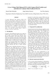
HERNANDEZ-GARDUNO AND SILVA-MARTINEZ: CONTINUOUS-TIME CMFB FOR HIGH-SPEED SWITCHED-CAPACITOR NETWORKS 1615Fig. 9.Second-order bandpass filter.the amplifier is then determined by (11), shown at the bottomof the page, which is well below 0 dB <strong>for</strong>TABLE IICAPACITOR VALUES FOR THE BANDPASS FILTERThe PSRR is inversely proportional to , and, <strong>for</strong> fixeddimensions of transistors M7a–M7d, it is inversely proportionalto the square root of the power dissipated by the CMFB. Thesimulated power supply rejection of the fully differential amplifierof Fig. 2 is also shown in Fig. 8. A 26-dB rejection was obtainedat the output along with the second-order harmonic previouslydiscussed in Section IV.VI. MEASUREMENT RESULTSTo compare the CMFB schemes, a second-order bandpassswitched-capacitor filter was designed with a center frequencyMHz, quality factor , and a master clockfrequency of 65 MHz. The filter’s schematic is shown in Fig. 9(where MHz, MHz, and denotes earlyphases). The capacitor values are included in Table II. Nonuni<strong>for</strong>msampling as described in [3] and [13] was used to reducethe capacitance spread. The same filter was implementedusing a conventional switched-capacitor CMFB and the proposedCMFB to compare their per<strong>for</strong>mance, keeping the restof the circuit the same. Both circuits were fabricated in TMSC0.35- m technology through the MOSIS Educational Program.The chip microphotograph is shown in Fig. 10.The measured frequency response of the bandpass filter designedwith the proposed CMFB is shown in Fig. 11. The relativeerror in the center frequency due to finite GBW and slew rate(i.e., dynamic error) versus different clock frequencies rangingfrom 40 to 80 MHz is shown in Fig. 12. For this test, the staticerrors ( and ) due to fringe capacitances and capacitormismatches were removed by measuring the error when the(10)(11)
1616 IEEE JOURNAL OF SOLID-STATE CIRCUITS, VOL. 40, NO. 8, AUGUST 2005Fig. 10. Chip microphotograph. (a) Filter A uses SC-CMFB. (b) Filter B usesproposed CMFB.Fig. 12. Filter’s experimental results: error in center frequency versus clockfrequency.Fig. 11.Frequency response of bandpass filter with the proposed CMFB.filter operates at low clock frequencies. The same tests were per<strong>for</strong>med<strong>for</strong> the bandpass filter using the conventional SC-CMFB(with pF and fF). The error starts to increasedrastically when using the SC-CMFB, while kept relativelysmall (below 1%) <strong>for</strong> faster clock frequencies (up to 72MHz) when using the proposed CMFB, proving the proposedCMFB to be more suitable <strong>for</strong> high-speed applications. The IM3(with two tones of dBm each) versus different clock frequencieswas measured <strong>for</strong> both filters, and the results are shownin Fig. 13. The filter with the continuous-time CMFB shows aslightly superior per<strong>for</strong>mance by approximately 1.5 dB at thenominal clock frequency of 65 MHz. As the clock frequencygoes beyond 80 MHz, both filters exhibit similar IM3 per<strong>for</strong>mancebecause the distortion is dominated by the on-resistanceof the switches rather than by the amplifier or the CMFB.The PSRR of the filter with the SC-CMFB is 1.5 dB whilethat with the proposed CMFB is 22 dB, which is a significant improvement.The filter with the continuous-time CMFB showeda worse CMRR by 5.5 dB than that with the SC-CMFB, butits CMRR and PSRR can be further improved by increasingFig. 13.Filter’s experimental results: IM3 versus clock frequency.(provided that is connected to a clean ground reference).A comparison of the experimental results of the two filtersis summarized in Table III. It is worth mentioning that, whilethe proposed CMFB increases the power consumption, the sameper<strong>for</strong>mance cannot be achieved if this additional power is usedin the amplifier while keeping the SC-CMFB. Besides havinga poor PSRR , increasing the bias current reduces the amplifier’sdc gain (increasing errors in and ), and thelarger output devices needed to keep the output swing reducethe frequency of the nondominant poles, degrading the differential-modeGBW and phase margin.VII. CONCLUSIONA continuous-time common-mode feedback circuit has beenproposed. Its reduced input capacitance loading the output ofthe amplifier improves the achievable gain–bandwidth product,
HERNANDEZ-GARDUNO AND SILVA-MARTINEZ: CONTINUOUS-TIME CMFB FOR HIGH-SPEED SWITCHED-CAPACITOR NETWORKS 1617TABLE IIICOMPARISON OF THE FILTER PERFORMANCE FOR THE TWO CMFB CIRCUITS[9] S. Azuma, S. Kawama, K. Iizuka, M. Miyamoto, and D. Senderowicz,“Embedded anti-aliasing in switched-capacitor ladder filters with variablegain and offset compensation,” IEEE J. Solid-State Circuits, vol.370, no. 3, pp. 349–356, Mar. 2002.[10] R. Castello and P. R. Gray, “A high-per<strong>for</strong>mance micropower switchedcapacitorfilter,” IEEE J. Solid-State Circuits, vol. SSC-20, no. 6, pp.1122–1132, Dec. 1985.[11] O. Choksi and L. R. Carley, “Analysis of switched-capacitor commonmodefeedback circuit,” IEEE Trans. Circuits Syst. II: Analog Digit.Signal Process., vol. 50, no. 12, pp. 906–917, Dec. 2003.[12] J. Silva-Martinez, “Effect of the transistor mismatches on the per<strong>for</strong>manceof fully-differential OTAs,” in Proc. IEEE Int. Symp. Circuits andSystems, vol. 5, Jun. 2003, pp. 253–256.[13] J. L. Ausin et al., “Switched-capacitor circuits with periodical nonuni<strong>for</strong>mindividual sampling,” IEEE Trans. Circuits Syst. II: Analog Digit.Signal Process., vol. 50, no. 8, pp. 404–414, Aug. 2003.making it more suitable <strong>for</strong> high-speed applications whencompared with the conventional switched-capacitor-basedCMFB and extending the limit on the clock frequenciesthat can be used <strong>for</strong> a particular technology. A second-order10.7-MHz bandpass filter was designed to compare the twoCMFB circuits. The settling-time error introduced by the finiteGBW of the amplifiers is significantly reduced when using theproposed CMFB. The third-order intermodulation distortionof both circuits is comparable, showing that the linearity ofthe proposed continuous-time CMFB is sufficient <strong>for</strong> typicalswitched-capacitor applications. Additionally, it provides aPSRR better than 22 dB, compared to 1.5 dB obtained whenusing the conventional SC-CMFB.REFERENCES[1] L. Yao, M. S. J. Steyaert, and W. Sansen, “A 1-V 140-W 88-dB audiosigma-delta modulator in 90-nm CMOS,” IEEE J. Solid-State Circuits,vol. 39, no. 11, pp. 1809–1818, Nov. 2004.[2] L. Wang and S. H. K. Embabi, “Low-voltage high-speed switched-capacitorcircuits without voltage bootstrapper,” IEEE J. Solid-State Circuits,vol. 38, no. 8, pp. 1411–1415, Aug. 2003.[3] J. Silva-Martinez et al., “A 58 dB SNR 6th order broadband 10.7 MHzSC ladder filter,” in Proc. IEEE Custom Integrated Circuits Conf., Sep.2003, pp. 13–16.[4] R. Gaggl, A. Wiesbauer, G. Fritz, C. Schranz, and P. Pessl, “A 85-dBdynamic range multibit Delta—Sigma ADC <strong>for</strong> ADSL-CO applicationsin 0.18-m CMOS,” IEEE J. Solid-State Circuits, vol. 38, no. 7, pp.1105–1114, Jul. 2003.[5] J. F. Duque-Carrillo, “<strong>Continuous</strong>-time common-mode feedback networks<strong>for</strong> fully-differential amplifiers: A comparative study,” in Proc.IEEE Int. Symp. Circuits and Systems, vol. 2, May 1993, pp. 1267–1270.[6] T. Pasch, U. Kleine, and R. Klinke, “A low voltage differential opampwith novel common mode feedback,” in Proc. IEEE Int. Conf. Electronics,Circuits and Systems, vol. 2, Sep. 1998, pp. 345–348.[7] M. Banu, J. M. Khoury, and Y. Tsividis, “Fully differential operationalamplifiers with accurate output balancing,” IEEE J. Solid-State Circuits,vol. SSC-23, no. 6, pp. 1410–1414, Dec. 1988.[8] D. Johns and K. Martin, Analog Integrated Circuit Design. New York:Wiley, 1997, pp. 287–291.David Hernandez-Garduno (S’00) was born inMexico City, Mexico. He received the B.S. degree inelectronics and communications (with honors) fromthe Universidad Iberoamericana, México, in 1998.He is currently working toward the Ph.D. degree atTexas A&M University, College Station.From 1998 to 2000, he was an RF Designer withKbTel Telecommunications, Mexico. In 2000, he wasawarded with the Fulbright-Conacyt scholarship topursue graduate studies in the U.S. In 2003, he wasan intern IC Designer working on RF oscillators <strong>for</strong>GPS systems with the RF/Wireless Group, Texas Instruments, Dallas, TX. Hisresearch interests include the design of analog/RF and broadband integrated circuits.Jose Silva-Martinez (SM’98) was born in Tecamachalco,Puebla, México. He received theB.S. degree in electronics from the UniversidadAutónoma de Puebla, México, in 1979, the M.Sc.degree from the Instituto Nacional de AstrofísicaOptica y Electrónica (INAOE), Puebla, México, in1981, and the Ph.D. degree from the KatholiekeUnivesiteit Leuven, Leuven, Belgium, in 1992.From 1981 to 1983, he was with the ElectricalEngineering Department, INAOE, where he wasinvolved with switched-capacitor circuit design.In 1983, he joined the Department of Electrical Engineering, UniversidadAutónoma de Puebla, where he remained until 1993; he was a co-founderof the graduate program on Opto-Electronics in 1992. From 1985 to 1986,he was a Visiting Scholar with the Electrical Engineering Department, TexasA&M University, College Station. In 1993, he rejoined the Electronics Department,INAOE, and, from May 1995 to December 1998, was the Head ofthe Electronics Department, and he was a cofounder of the Ph.D. program inelectronics in 1993. He is currently with the Analog and Mixed Signal Center,Department of Electrical Engineering, Texas A&M University, where he holdsthe position of Associate Professor. His current field of research is in the designand fabrication of integrated circuits <strong>for</strong> communications and biomedicalapplications.Dr. Silva-Martínez has served as IEEE Circuits and Systems SocietyVice President Region 9 (1997–1998) and as Associate Editor <strong>for</strong> the IEEETRANSACTIONS ON CIRCUITS AND SYSTEMS II from 1997 to 1998 and May2002 to December 2003. Since January 2004, he has been serving as AssociateEditor of the IEEE TRANSACTIONS ON CIRCUITS AND SYSTEMS I. He was themain organizer of the 1998 and 1999 International IEEE-CAS Tours in Region9 and Chairman of the International Workshop on Mixed-<strong>Mode</strong> IC Design andApplications (1997–1999). He is the inaugural holder of the TI Professorship-Iin Analog Engineering, Texas A&M University. He was a corecipient of the1990 European Solid-State Circuits Conference Best Paper Award.