74AHC573; 74AHCT573 Octal D-type transparant latch; 3-state
74AHC573; 74AHCT573 Octal D-type transparant latch; 3-state
74AHC573; 74AHCT573 Octal D-type transparant latch; 3-state
Create successful ePaper yourself
Turn your PDF publications into a flip-book with our unique Google optimized e-Paper software.
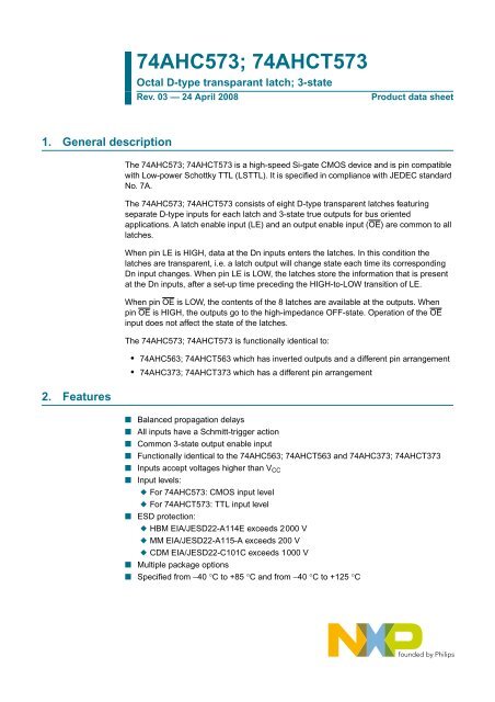
<strong>74AHC573</strong>; <strong>74AHCT573</strong><strong>Octal</strong> D-<strong>type</strong> <strong>transparant</strong> <strong>latch</strong>; 3-<strong>state</strong>Rev. 03 — 24 April 2008Product data sheet1. General description2. FeaturesThe <strong>74AHC573</strong>; <strong>74AHCT573</strong> is a high-speed Si-gate CMOS device and is pin compatiblewith Low-power Schottky TTL (LSTTL). It is specified in compliance with JEDEC standardNo. 7A.The <strong>74AHC573</strong>; <strong>74AHCT573</strong> consists of eight D-<strong>type</strong> transparent <strong>latch</strong>es featuringseparate D-<strong>type</strong> inputs for each <strong>latch</strong> and 3-<strong>state</strong> true outputs for bus orientedapplications. A <strong>latch</strong> enable input (LE) and an output enable input (OE) are common to all<strong>latch</strong>es.When pin LE is HIGH, data at the Dn inputs enters the <strong>latch</strong>es. In this condition the<strong>latch</strong>es are transparent, i.e. a <strong>latch</strong> output will change <strong>state</strong> each time its correspondingDn input changes. When pin LE is LOW, the <strong>latch</strong>es store the information that is presentat the Dn inputs, after a set-up time preceding the HIGH-to-LOW transition of LE.When pin OE is LOW, the contents of the 8 <strong>latch</strong>es are available at the outputs. Whenpin OE is HIGH, the outputs go to the high-impedance OFF-<strong>state</strong>. Operation of the OEinput does not affect the <strong>state</strong> of the <strong>latch</strong>es.The <strong>74AHC573</strong>; <strong>74AHCT573</strong> is functionally identical to:• 74AHC563; 74AHCT563 which has inverted outputs and a different pin arrangement• 74AHC373; 74AHCT373 which has a different pin arrangement■ Balanced propagation delays■ All inputs have a Schmitt-trigger action■ Common 3-<strong>state</strong> output enable input■ Functionally identical to the 74AHC563; 74AHCT563 and 74AHC373; 74AHCT373■ Inputs accept voltages higher than V CC■ Input levels:◆ For <strong>74AHC573</strong>: CMOS input level◆ For <strong>74AHCT573</strong>: TTL input level■ ESD protection:◆ HBM EIA/JESD22-A114E exceeds 2000 V◆ MM EIA/JESD22-A115-A exceeds 200 V◆ CDM EIA/JESD22-C101C exceeds 1000 V■ Multiple package options■ Specified from −40 °C to +85 °C and from −40 °C to +125 °C
NXP Semiconductors<strong>74AHC573</strong>; <strong>74AHCT573</strong><strong>Octal</strong> D-<strong>type</strong> <strong>transparant</strong> <strong>latch</strong>; 3-<strong>state</strong>5. Pinning information5.1 PinningOE120V CCD0219Q0D1318Q1D2417Q2D3D4565731615Q3Q4D5714Q5D6813Q6D7912Q7GND1011LE001aad099Fig 5.Pin configuration SO20 and TSSOP205.2 Pin descriptionTable 2. Pin descriptionSymbol Pin DescriptionOE 1 3-<strong>state</strong> output enable input (active LOW)D0 2 data input 0D1 3 data input 1D2 4 data input 2D3 5 data input 3D4 6 data input 4D5 7 data input 5D6 8 data input 6D7 9 data input 7GND 10 ground (0 V)LE 11 <strong>latch</strong> enable input (active HIGH)Q7 12 3-<strong>state</strong> <strong>latch</strong> output 7Q6 13 3-<strong>state</strong> <strong>latch</strong> output 6Q5 14 3-<strong>state</strong> <strong>latch</strong> output 5Q4 15 3-<strong>state</strong> <strong>latch</strong> output 4Q3 16 3-<strong>state</strong> <strong>latch</strong> output 3Q2 17 3-<strong>state</strong> <strong>latch</strong> output 2Q1 18 3-<strong>state</strong> <strong>latch</strong> output 1Q0 19 3-<strong>state</strong> <strong>latch</strong> output 0V CC 20 supply voltage74AHC_AHCT573_3© NXP B.V. 2008. All rights reserved.Product data sheet Rev. 03 — 24 April 2008 4 of 17
NXP Semiconductors<strong>74AHC573</strong>; <strong>74AHCT573</strong><strong>Octal</strong> D-<strong>type</strong> <strong>transparant</strong> <strong>latch</strong>; 3-<strong>state</strong>6. Functional descriptionTable 3. Function table [1]Operating mode Input Internal <strong>latch</strong> Output[1] H = HIGH voltage level;h = HIGH voltage level one set-up time prior to the HIGH-to-LOW LE transition;L = LOW voltage level;l = LOW voltage level one set-up time prior to the HIGH-to-LOW LE transition;Z = high-impedance OFF-<strong>state</strong>.7. Limiting valuesOE LE Dn Q0 to Q7Enable and read register (transparent L H L L Lmode)H H HLatch and read register L L l L Lh H HLatch register and disable outputs H L l L Zh H ZTable 4. Limiting valuesIn accordance with the Absolute Maximum Rating System (IEC 60134). Voltages are referenced to GND (ground = 0 V).Symbol Parameter Conditions Min Max UnitV CC supply voltage −0.5 +7.0 VV I input voltage −0.5 +7.0 VI IK input clamping current V I < −0.5 V[1]−20 - mAI OK output clamping current V O < −0.5 V or V O >V CC + 0.5 V[1]−20 +20 mAI O output current V O = −0.5 V to (V CC + 0.5 V) −25 +25 mAI CC supply current - +75 mAI GND ground current −75 - mAT stg storage temperature −65 +150 °CP tot total power dissipation T amb = −40 °C to +125 °C[2]- 500 mW[1] The input and output voltage ratings may be exceeded if the input and output current ratings are observed.[2] For SO20 packages: above 70 °C the value of P tot derates linearly at 8 mW/K.For TSSOP20 packages: above 60 °C the value of P tot derates linearly at 5.5 mW/K.74AHC_AHCT573_3© NXP B.V. 2008. All rights reserved.Product data sheet Rev. 03 — 24 April 2008 5 of 17
NXP Semiconductors<strong>74AHC573</strong>; <strong>74AHCT573</strong><strong>Octal</strong> D-<strong>type</strong> <strong>transparant</strong> <strong>latch</strong>; 3-<strong>state</strong>8. Recommended operating conditionsTable 5. Operating conditionsSymbol Parameter Conditions Min Typ Max Unit<strong>74AHC573</strong>V CC supply voltage 2.0 5.0 5.5 VV I input voltage 0 - 5.5 VV O output voltage 0 - V CC VT amb ambient temperature −40 +25 +125 °C∆t/∆V input transition rise and fall rate V CC = 3.0 V to 3.6 V - - 100 ns/VV CC = 4.5 V to 5.5 V - - 20 ns/V<strong>74AHCT573</strong>V CC supply voltage 4.5 5.0 5.5 VV I input voltage 0 - 5.5 VV O output voltage 0 - V CC VT amb ambient temperature −40 +25 +125 °C∆t/∆V input transition rise and fall rate V CC = 4.5 V to 5.5 V - - 20 ns/V9. Static characteristicsTable 6. Static characteristicsAt recommended operating conditions; voltages are referenced to GND (ground = 0 V).Symbol Parameter Conditions 25 °C −40 °C to +85 °C −40 °C to +125 °C Unit<strong>74AHC573</strong>V IH HIGH-levelinput voltageV ILV OHV OLLOW-levelinput voltageHIGH-leveloutput voltageLOW-leveloutput voltageMin Typ Max Min Max Min Typ MaxV CC = 2.0 V 1.5 - - 1.5 - 1.5 - - VV CC = 3.0 V 2.1 - - 2.1 - 2.1 - - VV CC = 5.5 V 3.85 - - 3.85 - 3.85 - - VV CC = 2.0 V - - 0.5 - 0.5 - - 0.5 VV CC = 3.0 V - - 0.9 - 0.9 - - 0.9 VV CC = 5.5 V - - 1.65 - 1.65 - - 1.65 VV I = V IH or V ILI O = −50 µA; V CC = 2.0 V 1.9 2.0 - 1.9 - 1.9 - - VI O = −50 µA; V CC = 3.0 V 2.9 3.0 - 2.9 - 2.9 - - VI O = −50 µA; V CC = 4.5 V 4.4 4.5 - 4.4 - 4.4 - - VI O = −4.0 mA; V CC = 3.0 V 2.58 - - 2.48 - 2.40 - - VI O = −8.0 mA; V CC = 4.5 V 3.94 - - 3.80 - 3.70 - - VV I = V IH or V ILI O = 50 µA; V CC = 2.0 V - 0 0.1 - 0.1 - - 0.1 VI O = 50 µA; V CC = 3.0 V - 0 0.1 - 0.1 - - 0.1 VI O = 50 µA; V CC = 4.5 V - 0 0.1 - 0.1 - - 0.1 VI O = 4.0 mA; V CC = 3.0 V - - 0.36 - 0.44 - - 0.55 VI O = 8.0 mA; V CC = 4.5 V - - 0.36 - 0.44 - - 0.55 V74AHC_AHCT573_3© NXP B.V. 2008. All rights reserved.Product data sheet Rev. 03 — 24 April 2008 6 of 17
NXP Semiconductors<strong>74AHC573</strong>; <strong>74AHCT573</strong><strong>Octal</strong> D-<strong>type</strong> <strong>transparant</strong> <strong>latch</strong>; 3-<strong>state</strong>Table 6. Static characteristics …continuedAt recommended operating conditions; voltages are referenced to GND (ground = 0 V).Symbol Parameter Conditions 25 °C −40 °C to +85 °C −40 °C to +125 °C UnitI OZI IOFF-<strong>state</strong>output currentinput leakagecurrentV I =V IH or V IL ;V O =V CC or GND;V CC = 5.5 VV I =V CC or GND;V CC = 0 V to 5.5 V- - ±0.25 - ±2.5 - - ±10.0 µA- - 0.1 - 1.0 - - 2.0 µAI CC supply current V I =V CC or GND; I O =0A; - - 4.0 - 40 - - 80 µAV CC = 5.5 VC I input V I =V CC or GND - 3 10 - 10 - - 10 pFcapacitanceC O output- 4 - - - - - 10 pFcapacitance<strong>74AHCT573</strong>V IH HIGH-level V CC = 4.5 V to 5.5 V 2.0 - - 2.0 - 2.0 - - Vinput voltageV IL LOW-level V CC = 4.5 V to 5.5 V - - 0.8 - 0.8 - - 0.8 Vinput voltageV OH HIGH-leveloutput voltageV I = V IH or V IL ; V CC = 4.5 VI O = −50 µA 4.4 4.5 - 4.4 - 4.4 - - VI O = −8.0 mA 3.94 - - 3.80 - 3.70 - - VV OL LOW-leveloutput voltageV I = V IH or V IL ; V CC = 4.5 VI O = 50 µA - 0 0.1 - 0.1 - - 0.1 VI O = 8.0 mA - - 0.36 - 0.44 - - 0.55 VI OZI IOFF-<strong>state</strong>output currentinput leakagecurrentV I =V IH or V IL ;V O =V CC or GND per inputpin; other inputs at V CC orGND; I O =0 AV I = 5.5 V or GND;V CC = 0 V to 5.5 VI CC supply current V I =V CC or GND; I O = 0 A;V CC = 5.5 V∆I CCC IC Oadditionalsupply currentinputcapacitanceoutputcapacitanceper input pin;V I =V CC − 2.1 V; I O = 0 A;other pins at V CC or GND;V CC = 4.5 V to 5.5 VMin Typ Max Min Max Min Typ Max- - ±0.25 - ±2.5 - - ±10.0 µA- - 0.1 - 1.0 - - 2.0 µA- - 4.0 - 40 - - 80 µA- - 1.35 - 1.5 - - 1.5 mAV I =V CC or GND - 3 10 - 10 - - 10 pF- 4 - - - - - 10 pF74AHC_AHCT573_3© NXP B.V. 2008. All rights reserved.Product data sheet Rev. 03 — 24 April 2008 7 of 17
NXP Semiconductors<strong>74AHC573</strong>; <strong>74AHCT573</strong><strong>Octal</strong> D-<strong>type</strong> <strong>transparant</strong> <strong>latch</strong>; 3-<strong>state</strong>10. Dynamic characteristicsTable 7. Dynamic characteristicsVoltages are referenced to GND (ground = 0 V); for test circuit see Figure 10.Symbol Parameter Conditions 25 °C −40 °C to +85 °C −40 °C to +125 °C UnitMin Typ [1] Max Min Max Min Max<strong>74AHC573</strong>t pd propagation Dn to Qn; see Figure 6[2]delayV CC = 3.0 V to 3.6 VC L = 15 pF - 5.5 11.0 1.0 13.0 1.0 14.0 nsC L = 50 pF - 7.8 14.5 1.0 16.5 1.0 18.5 nsV CC = 4.5 V to 5.5 VC L = 15 pF - 3.9 6.8 1.0 8.0 1.0 8.5 nsC L = 50 pF - 5.5 8.8 1.0 10.0 1.0 11.0 nsLE to Qn; see Figure 7 [2]V CC = 3.0 V to 3.6 VC L = 15 pF - 5.8 11.9 1.0 14.0 1.0 15.0 nsC L = 50 pF - 8.3 15.4 1.0 17.5 1.0 19.5 nsV CC = 4.5 V to 5.5 VC L = 15 pF - 4.2 7.7 1.0 9.0 1.0 10.0 nsC L = 50 pF - 5.9 9.7 1.0 11.0 1.0 12.5 nst en enable time OE to Qn; see Figure 8[3]V CC = 3.0 V to 3.6 VC L = 15 pF - 5.8 11.5 1.0 13.5 1.0 14.5 nsC L = 50 pF - 8.3 15.0 1.0 17.0 1.0 19.0 nsV CC = 4.5 V to 5.5 VC L = 15 pF - 4.4 7.7 1.0 9.0 1.0 10.0 nsC L = 50 pF - 6.3 9.7 1.0 11.0 1.0 12.5 nst dis disable time OE to Qn; see Figure 8[4]V CC = 3.0 V to 3.6 VC L = 15 pF - 6.8 11.0 1.0 13.0 1.0 14.0 nsC L = 50 pF - 9.7 14.5 1.0 16.5 1.0 18.5 nsV CC = 4.5 V to 5.5 VC L = 15 pF - 4.6 7.7 1.0 9.0 1.0 10.0 nsC L = 50 pF - 7.4 9.7 1.0 11.0 1.0 12.5 nst W pulse width LE HIGH; see Figure 7V CC = 3.0 V to 3.6 V 5.0 - - 5.0 - 5.0 - nsV CC = 4.5 V to 5.5 V 5.0 - - 5.0 - 5.0 - nst su set-up time Dn to LE; see Figure 9V CC = 3.0 V to 3.6 V 3.5 - - 3.5 - 3.5 - nsV CC = 4.5 V to 5.5 V 3.5 - - 3.5 - 3.5 - ns74AHC_AHCT573_3© NXP B.V. 2008. All rights reserved.Product data sheet Rev. 03 — 24 April 2008 8 of 17
NXP Semiconductors<strong>74AHC573</strong>; <strong>74AHCT573</strong><strong>Octal</strong> D-<strong>type</strong> <strong>transparant</strong> <strong>latch</strong>; 3-<strong>state</strong>Table 7. Dynamic characteristics …continuedVoltages are referenced to GND (ground = 0 V); for test circuit see Figure 10.Symbol Parameter Conditions 25 °C −40 °C to +85 °C −40 °C to +125 °C Unitt h hold time Dn to LE; see Figure 9V CC = 3.0 V to 3.6 V 1.5 - - 1.5 - 1.5 - nsV CC = 4.5 V to 5.5 V 1.5 - - 1.5 - 1.5 - nsC PDpowerdissipationcapacitancef i = 1 MHz;[5]- 12 - - - - - pFV I = GND to V CC<strong>74AHCT573</strong>; V CC = 4.5 V to 5.5 Vt pd propagation Dn to Qn; see Figure 6[2]delayC L = 15 pF - 3.5 5.5 1 6.5 1 7.0 nsC L = 50 pF - 4.9 7.5 1 8.5 1 9.5 nsLE to Qn; see Figure 7[2]C L = 15 pF - 3.9 6.0 1 7.0 1 7.5 nsC L = 50 pF - 5.5 8.5 1 9.5 1 11.0 nst en enable time OE to Qn; see Figure 8[3]C L = 15 pF - 4.1 6.5 1 7.5 1 8.5 nsC L = 50 pF - 5.9 8.5 1 10.0 1 11.0 nst dis disable time OE to Qn; see Figure 8[4]C L = 15 pF - 4.5 6.5 1 7.5 1 8.5 nsC L = 50 pF - 6.4 9.0 1 10.0 1 11.5 nst W pulse width LE HIGH; see Figure 7 5.0 - - 5.0 - 5.0 - nst su set-up time Dn to LE; see Figure 9 3.5 - - 3.5 - 3.5 - nst h hold time Dn to LE; see Figure 9 1.5 - - 1.5 - 1.5 - nsC PDpowerdissipationcapacitancef i = 1 MHz;[5]- 18 - - - - - pFV I = GND to V CC[1] Typical values are measured at nominal supply voltage (V CC = 3.3 V and V CC = 5.0 V).[2] t pd is the same as t PHL and t PLH .[3] t en is the same as t PZH and t PZL .[4] t dis is the same as t PHZ and t PLZ .[5] C PD is used to determine the dynamic power dissipation (P D in µW).P D =C PD × V 2 CC × f i × N+Σ(C L × V 2 CC × f o ) where:f i = input frequency in MHz;f o = output frequency in MHz;C L = output load capacitance in pF;V CC = supply voltage in V;N = number of inputs switching;Σ(C L × V 2 CC × f o ) = sum of the outputs.Min Typ [1] Max Min Max Min Max74AHC_AHCT573_3© NXP B.V. 2008. All rights reserved.Product data sheet Rev. 03 — 24 April 2008 9 of 17
NXP Semiconductors<strong>74AHC573</strong>; <strong>74AHCT573</strong><strong>Octal</strong> D-<strong>type</strong> <strong>transparant</strong> <strong>latch</strong>; 3-<strong>state</strong>11. WaveformsV IDn inputV MGNDt PHLt PLHV OHQn outputV MV OLmna811Fig 6.Measurement points are given in Table 8.V OL and V OH are typical voltage output levels that occur with the output load.Data input to output propagation delays1/f maxV ILE inputV MGNDt Wt PHL t PLHV OHQn output V MV OLmna812Fig 7.V OL and V OH are typical voltage output levels that occur with the output load.Latch enable input to output propagation delays74AHC_AHCT573_3© NXP B.V. 2008. All rights reserved.Product data sheet Rev. 03 — 24 April 2008 10 of 17
NXP Semiconductors<strong>74AHC573</strong>; <strong>74AHCT573</strong><strong>Octal</strong> D-<strong>type</strong> <strong>transparant</strong> <strong>latch</strong>; 3-<strong>state</strong>OE inputQn outputLOW-to-OFFOFF-to-LOWGNDV CCV IV OLV Mt PLZV Xt PZLt PHZt PZHV OHQn outputHIGH-to-OFFOFF-to-HIGHGNDoutputsenabledV YoutputsdisabledV MV Moutputsenabledmna813Fig 8.Measurement points are given in Table 8.V OL and V OH are typical voltage output levels that occur with the output load.Enable and disable timesV IDn inputV MGNDt ht ht sut suV ILE inputV MGNDmna814Fig 9.Measurement points are given in Table 8.V OL and V OH are typical voltage output levels that occur with the output load.The shaded areas indicate when the input is permitted to change for predicable output performance.Data set-up and hold timesTable 8. Measurement pointsType Input OutputV M V M V X V Y<strong>74AHC573</strong> 0.5 × V CC 0.5 × V CC V OL + 0.3 V V OH − 0.3 V<strong>74AHCT573</strong> 1.5 V 0.5 × V CC V OL + 0.3 V V OH − 0.3 V74AHC_AHCT573_3© NXP B.V. 2008. All rights reserved.Product data sheet Rev. 03 — 24 April 2008 11 of 17
NXP Semiconductors<strong>74AHC573</strong>; <strong>74AHCT573</strong><strong>Octal</strong> D-<strong>type</strong> <strong>transparant</strong> <strong>latch</strong>; 3-<strong>state</strong>V Inegativepulse0 V90 %V M10 %t WV Mt ft rt rt fV Ipositivepulse0 V10 %90 %V Mt WV MV CCV CCGVIDUTVORLS1openRTCL001aad983Fig 10.Test data is given in Table 9.Definitions test circuit:R T = termination resistance should be equal to output impedance Z o of the pulse generator.C L = load capacitance including jig and probe capacitance.R L = load resistance.S1 = test selection switch.Test circuitry for switching timesTable 9. Test dataType Input Load S1 positionV I t r , t f C L R L t PHL , t PLH t PZH , t PHZ t PZL , t PLZ<strong>74AHC573</strong> V CC ≤ 3.0 ns 15 pF, 50 pF 1 kΩ open GND V CC<strong>74AHCT573</strong> 3.0 V ≤ 3.0 ns 15 pF, 50 pF 1 kΩ open GND V CC74AHC_AHCT573_3© NXP B.V. 2008. All rights reserved.Product data sheet Rev. 03 — 24 April 2008 12 of 17
NXP Semiconductors<strong>74AHC573</strong>; <strong>74AHCT573</strong><strong>Octal</strong> D-<strong>type</strong> <strong>transparant</strong> <strong>latch</strong>; 3-<strong>state</strong>12. Package outlineSO20: plastic small outline package; 20 leads; body width 7.5 mmSOT163-1DEAXcyv MAZ2011H EQA 2A 1L p(A ) 3Apin 1 indexθL1eb p10w Mdetail X0 5 10 mmscaleDIMENSIONS (inch dimensions are derived from the original mm dimensions)UNITmminchesAmax.2.650.1A 1 A 2 A 3 b p c D (1) E (1) e H (1)E L L p Q v w y Z0.30.10.0120.0042.452.250.0960.0890.250.010.490.360.0190.0140.320.230.0130.00913.012.60.510.497.67.40.300.291.2710.6510.00Note1. Plastic or metal protrusions of 0.15 mm (0.006 inch) maximum per side are not included.0.050.4190.3941.40.0551.10.40.0430.0161.11.00.0430.0390.250.25 0.10.01 0.01 0.004θ0.90.4 o8o0.035 00.016OUTLINEVERSIONREFERENCESIEC JEDEC JEITAEUROPEANPROJECTIONISSUE DATESOT163-1075E04 MS-01399-12-2703-02-19Fig 11.Package outline SOT163-1 (SO20)74AHC_AHCT573_3© NXP B.V. 2008. All rights reserved.Product data sheet Rev. 03 — 24 April 2008 13 of 17
NXP Semiconductors<strong>74AHC573</strong>; <strong>74AHCT573</strong><strong>Octal</strong> D-<strong>type</strong> <strong>transparant</strong> <strong>latch</strong>; 3-<strong>state</strong>TSSOP20: plastic thin shrink small outline package; 20 leads; body width 4.4 mmSOT360-1yDcH EEAXv MAZ20 11pin 1 indexQA 2A 1L p(A ) 3Aθ1 10w Meb pLdetail X0 2.5 5 mmscaleDIMENSIONS (mm are the original dimensions)AUNIT A 1 A 2 A 3 b p c D (1) E (2) e H (1)E L L p Q v w y Zmax.mm1.10.150.050.950.800.250.300.190.20.16.66.44.54.30.656.66.210.750.500.40.30.20.13 0.10.50.2θo8o0Notes1. Plastic or metal protrusions of 0.15 mm maximum per side are not included.2. Plastic interlead protrusions of 0.25 mm maximum per side are not included.OUTLINEVERSIONREFERENCESIEC JEDEC JEITASOT360-1 MO-153EUROPEANPROJECTIONISSUE DATE99-12-2703-02-19Fig 12.Package outline SOT360-1 (TSSOP20)74AHC_AHCT573_3© NXP B.V. 2008. All rights reserved.Product data sheet Rev. 03 — 24 April 2008 14 of 17
NXP Semiconductors<strong>74AHC573</strong>; <strong>74AHCT573</strong><strong>Octal</strong> D-<strong>type</strong> <strong>transparant</strong> <strong>latch</strong>; 3-<strong>state</strong>13. AbbreviationsTable 10.AcronymCDMCMOSESDHBMMMTTLAbbreviationsDescriptionCharged Device ModelComplementary Metal-Oxide SemiconductorElectroStatic DischargeHuman Body ModelMachine ModelTransistor-Transistor Logic14. Revision historyTable 11.Revision historyDocument ID Release date Data sheet status Change notice Supersedes74AHC_AHCT573_3 20080424 Product data sheet - 74AHC_AHCT573_2Modifications:• The format of this data sheet has been redesigned to comply with the new identityguidelines of NXP Semiconductors.• Legal texts have been adapted to the new company name where appropriate.• Table 6: conditions for the input leakage current have been changed.74AHC_AHCT573_2 20031208 Product specification - 74AHC_AHCT573_174AHC_AHCT573_1 19990927 Product specification - -74AHC_AHCT573_3© NXP B.V. 2008. All rights reserved.Product data sheet Rev. 03 — 24 April 2008 15 of 17
NXP Semiconductors<strong>74AHC573</strong>; <strong>74AHCT573</strong><strong>Octal</strong> D-<strong>type</strong> <strong>transparant</strong> <strong>latch</strong>; 3-<strong>state</strong>15. Legal information15.1 Data sheet statusDocument status [1][2] Product status [3] DefinitionObjective [short] data sheet Development This document contains data from the objective specification for product development.Preliminary [short] data sheet Qualification This document contains data from the preliminary specification.Product [short] data sheet Production This document contains the product specification.[1] Please consult the most recently issued document before initiating or completing a design.[2] The term ‘short data sheet’ is explained in section “Definitions”.[3] The product status of device(s) described in this document may have changed since this document was published and may differ in case of multiple devices. The latest product statusinformation is available on the Internet at URL http://www.nxp.com.15.2 DefinitionsDraft — The document is a draft version only. The content is still underinternal review and subject to formal approval, which may result inmodifications or additions. NXP Semiconductors does not give anyrepresentations or warranties as to the accuracy or completeness ofinformation included herein and shall have no liability for the consequences ofuse of such information.Short data sheet — A short data sheet is an extract from a full data sheetwith the same product <strong>type</strong> number(s) and title. A short data sheet is intendedfor quick reference only and should not be relied upon to contain detailed andfull information. For detailed and full information see the relevant full datasheet, which is available on request via the local NXP Semiconductors salesoffice. In case of any inconsistency or conflict with the short data sheet, thefull data sheet shall prevail.15.3 DisclaimersGeneral — Information in this document is believed to be accurate andreliable. However, NXP Semiconductors does not give any representations orwarranties, expressed or implied, as to the accuracy or completeness of suchinformation and shall have no liability for the consequences of use of suchinformation.Right to make changes — NXP Semiconductors reserves the right to makechanges to information published in this document, including withoutlimitation specifications and product descriptions, at any time and withoutnotice. This document supersedes and replaces all information supplied priorto the publication hereof.Suitability for use — NXP Semiconductors products are not designed,authorized or warranted to be suitable for use in medical, military, aircraft,space or life support equipment, nor in applications where failure ormalfunction of an NXP Semiconductors product can reasonably be expectedto result in personal injury, death or severe property or environmentaldamage. NXP Semiconductors accepts no liability for inclusion and/or use ofNXP Semiconductors products in such equipment or applications andtherefore such inclusion and/or use is at the customer’s own risk.Applications — Applications that are described herein for any of theseproducts are for illustrative purposes only. NXP Semiconductors makes norepresentation or warranty that such applications will be suitable for thespecified use without further testing or modification.Limiting values — Stress above one or more limiting values (as defined inthe Absolute Maximum Ratings System of IEC 60134) may cause permanentdamage to the device. Limiting values are stress ratings only and operation ofthe device at these or any other conditions above those given in theCharacteristics sections of this document is not implied. Exposure to limitingvalues for extended periods may affect device reliability.Terms and conditions of sale — NXP Semiconductors products are soldsubject to the general terms and conditions of commercial sale, as publishedat http://www.nxp.com/profile/terms, including those pertaining to warranty,intellectual property rights infringement and limitation of liability, unlessexplicitly otherwise agreed to in writing by NXP Semiconductors. In case ofany inconsistency or conflict between information in this document and suchterms and conditions, the latter will prevail.No offer to sell or license — Nothing in this document may be interpretedor construed as an offer to sell products that is open for acceptance or thegrant, conveyance or implication of any license under any copyrights, patentsor other industrial or intellectual property rights.15.4 TrademarksNotice: All referenced brands, product names, service names and trademarksare the property of their respective owners.16. Contact informationFor more information, please visit: http://www.nxp.comFor sales office addresses, please send an email to: salesaddresses@nxp.com74AHC_AHCT573_3© NXP B.V. 2008. All rights reserved.Product data sheet Rev. 03 — 24 April 2008 16 of 17
NXP Semiconductors<strong>74AHC573</strong>; <strong>74AHCT573</strong><strong>Octal</strong> D-<strong>type</strong> <strong>transparant</strong> <strong>latch</strong>; 3-<strong>state</strong>17. Contents1 General description . . . . . . . . . . . . . . . . . . . . . . 12 Features . . . . . . . . . . . . . . . . . . . . . . . . . . . . . . . 13 Ordering information . . . . . . . . . . . . . . . . . . . . . 24 Functional diagram . . . . . . . . . . . . . . . . . . . . . . 25 Pinning information . . . . . . . . . . . . . . . . . . . . . . 45.1 Pinning . . . . . . . . . . . . . . . . . . . . . . . . . . . . . . . 45.2 Pin description . . . . . . . . . . . . . . . . . . . . . . . . . 46 Functional description . . . . . . . . . . . . . . . . . . . 57 Limiting values. . . . . . . . . . . . . . . . . . . . . . . . . . 58 Recommended operating conditions. . . . . . . . 69 Static characteristics. . . . . . . . . . . . . . . . . . . . . 610 Dynamic characteristics . . . . . . . . . . . . . . . . . . 811 Waveforms . . . . . . . . . . . . . . . . . . . . . . . . . . . . 1012 Package outline . . . . . . . . . . . . . . . . . . . . . . . . 1313 Abbreviations . . . . . . . . . . . . . . . . . . . . . . . . . . 1514 Revision history . . . . . . . . . . . . . . . . . . . . . . . . 1515 Legal information. . . . . . . . . . . . . . . . . . . . . . . 1615.1 Data sheet status . . . . . . . . . . . . . . . . . . . . . . 1615.2 Definitions. . . . . . . . . . . . . . . . . . . . . . . . . . . . 1615.3 Disclaimers . . . . . . . . . . . . . . . . . . . . . . . . . . . 1615.4 Trademarks . . . . . . . . . . . . . . . . . . . . . . . . . . . 1616 Contact information. . . . . . . . . . . . . . . . . . . . . 1617 Contents . . . . . . . . . . . . . . . . . . . . . . . . . . . . . . 17Please be aware that important notices concerning this document and the product(s)described herein, have been included in section ‘Legal information’.© NXP B.V. 2008. All rights reserved.For more information, please visit: http://www.nxp.comFor sales office addresses, please send an email to: salesaddresses@nxp.comDate of release: 24 April 2008Document identifier: 74AHC_AHCT573_3


