DAC0830/DAC0831/DAC0832 8-Bit MuP Compatible, Double ...
DAC0830/DAC0831/DAC0832 8-Bit MuP Compatible, Double ...
DAC0830/DAC0831/DAC0832 8-Bit MuP Compatible, Double ...

You also want an ePaper? Increase the reach of your titles
YUMPU automatically turns print PDFs into web optimized ePapers that Google loves.
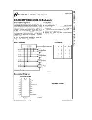
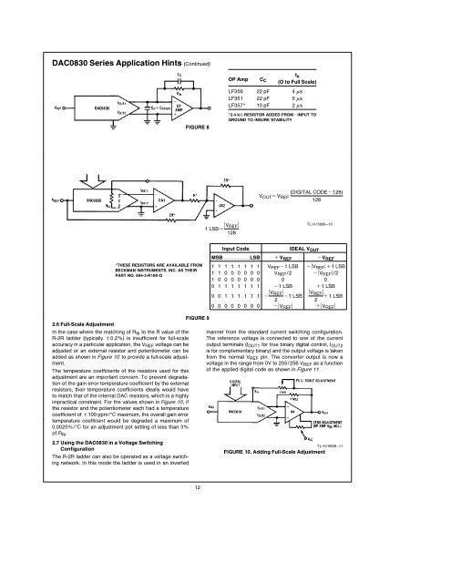
<strong>DAC0830</strong> Series Application Hints (Continued)t sOP Amp C C (O to Full Scale)LF356 22 pF 4 msLF351 22 pF 5 msLF357 10 pF 2 msFIGURE 824 kX RESISTOR ADDED FROMbINPUT TOGROUND TO INSURE STABILITYV OUT eV REF(DIGITAL CODEb128)1281 LSBe l V REFl128TLH5608–10Input CodeIDEAL V OUTMSB LSB aV REF bV REFTHESE RESISTORS ARE AVAILABLE FROM 1 1 1 1 1 1 1 1 V REF b1 LSB blV REFla1 LSBBECKMAN INSTRUMENTS INC AS THEIR1 1 0 0 0 0 0 0 V REF 2 blVPART NO 694-3-R10K-DREFl21 0 0 0 0 0 0 0 0 00 1 1 1 1 1 1 1 l b1 LSB a1 LSBV0 0 1 1 1 1 1 1 b REFlb1 l VLSB REFla1 LSB220 0 0 0 0 0 0 0 blV REFl alV REFlFIGURE 926 Full-Scale AdjustmentIn the case where the matching of R fb to the R value of theR-2R ladder (typically g02%) is insufficient for full-scaleaccuracy in a particular application the V REF voltage can beadjusted or an external resistor and potentiometer can beadded as shown in Figure 10 to provide a full-scale adjustmentThe temperature coefficients of the resistors used for thisadjustment are an important concern To prevent degradationof the gain error temperature coefficient by the externalresistors their temperature coefficients ideally would haveto match that of the internal DAC resistors which is a highlyimpractical constraint For the values shown in Figure 10 ifthe resistor and the potentiometer each had a temperaturecoefficient of g100 ppmC maximum the overall gain errortemperature coefficent would be degraded a maximum of00025%C for an adjustment pot setting of less than 3%of R fb 27 Using the <strong>DAC0830</strong> in a Voltage SwitchingConfigurationThe R-2R ladder can also be operated as a voltage switchingnetwork In this mode the ladder is used in an invertedmanner from the standard current switching configurationThe reference voltage is connected to one of the currentoutput terminals (I OUT1 for true binary digital control I OUT2is for complementary binary) and the output voltage is takenfrom the normal V REF pin The converter output is now avoltage in the range from 0V to 255256 V REF as a functionof the applied digital code as shown in Figure 11TLH5608–11FIGURE 10 Adding Full-Scale Adjustment12