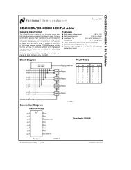
DAC0830/DAC0831/DAC0832 8-Bit MuP Compatible, Double ...
DAC0830/DAC0831/DAC0832 8-Bit MuP Compatible, Double ...
DAC0830/DAC0831/DAC0832 8-Bit MuP Compatible, Double ...

Create successful ePaper yourself
Turn your PDF publications into a flip-book with our unique Google optimized e-Paper software.
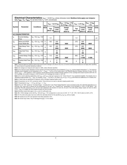
Electrical Characteristics V REF e10000 V DC unless otherwise noted Boldface limits apply over temperatureT MIN sT A sT MAX For all other limits T A e25C (Continued)Symbol Parameter ConditionsVV CC e1575 V CC e12 V DC g5% VDC VCC e475 V CC e5V DCto 15 V DCSeeDC g5% g5% LimitNoteTested DesignTested Design UnitsTypTypLimit LimitLimit Limit(Note 12)(Note 12)(Note 5) (Note 6) (Note 5) (Note 6)AC CHARACTERISTICSt s Current SettingTimeV IL e0V V IH e5V10 10 mst W Write and XFER V IL e0V V IH e5V 11 100 250 375 600Pulse Width Min 9 320 320 900 900t DS Data Setup Time V IL e0V V IH e5V 9100 250 375 600Min 320 320 900 900t DH Data Hold Time V IL e0V V IH e5V 30 509Min 30 50t CS Control Setup Time V IL e0V V IH e5V 9110 250 600 900Min 320 320 1100 1100t CH Control Hold Time V IL e0V V IH e5V 009 0 10 0Min 0 0Note 1 Absolute Maximum Ratings indicate limits beyond which damage to the device may occur DC and AC electrical specifications do not apply when operatingthe device beyond its specified operating conditionsNote 2 All voltages are measured with respect to GND unless otherwise specifiedNote 3 The maximum power dissipation must be derated at elevated temperatures and is dictated by T JMAX i JA and the ambient temperature T A The maximumallowable power dissipation at any temperature is P D e (T JMAX b T A )i JA or the number given in the Absolute Maximum Ratings whichever is lower For thisdevice T JMAX e 125C (plastic) or 150C (ceramic) and the typical junction-to-ambient thermal resistance of the J package when board mounted is 80CW Forthe N package this number increases to 100CW and for the V package this number is 120CWNote 4 For current switching applications both I OUT1 and I OUT2 must go to ground or the ‘‘Virtual Ground’’ of an operational amplifier The linearity error isdegraded by approximately V OS d V REF For example if V REF e 10Vthena1mVoffset V OS onI OUT1 or I OUT2 will introduce an additional 001% linearity errorNote 5 Tested limits are guaranteed to National’s AOQL (Average Outgoing Quality Level)Note 6 Guaranteed but not 100% production tested These limits are not used to calculate outgoing quality levelsNote 7 Guaranteed at V REF e g10 V DC and V REF e g1 V DC Note 8 The unit ‘‘FSR’’ stands for ‘‘Full Scale Range’’ ‘‘Linearity Error’’ and ‘‘Power Supply Rejection’’ specs are based on this unit to eliminate dependence on aparticular V REF value and to indicate the true performance of the part The ‘‘Linearity Error’’ specification of the <strong>DAC0830</strong> is ‘‘005% of FSR (MAX)’’ Thisguarantees that after performing a zero and full scale adjustment (see Sections 25 and 26) the plot of the 256 analog voltage outputs will each be within005%cV REF of a straight line which passes through zero and full scaleNote 9 Boldface tested limits apply to the LJ and LCJ suffix parts onlyNote 10 A 100nA leakage current with R fb e20k and V REF e10V corresponds to a zero error of (100c10 b9c20c103 )c10010 which is 002% of FSNote 11 The entire write pulse must occur within the valid data interval for the specified t W t DS t DH and t S to applyNote 12 Typicals are at 25C and represent most likely parametric normNote 13 Human body model 100 pF discharged through a 15 kX resistorns4