Effect of Polyimide Variation and its Curing Temperature on CMOS ...
Effect of Polyimide Variation and its Curing Temperature on CMOS ...
Effect of Polyimide Variation and its Curing Temperature on CMOS ...

Create successful ePaper yourself
Turn your PDF publications into a flip-book with our unique Google optimized e-Paper software.
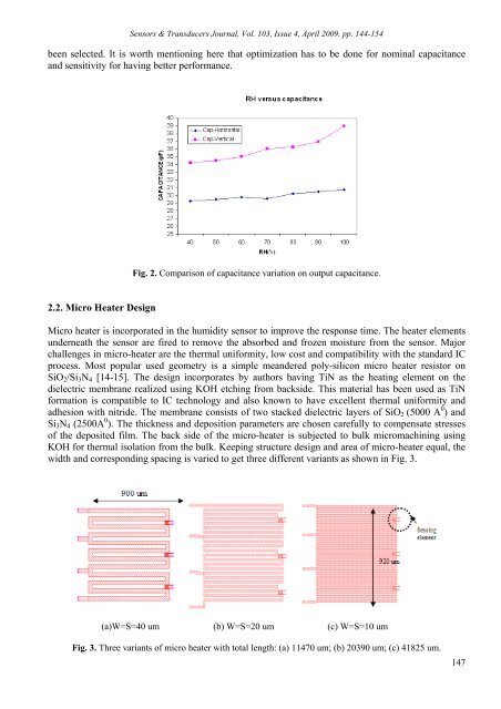
Sensors & Transducers Journal, Vol. 103, Issue 4, April 2009, pp. 144-154been selected. It is worth menti<strong>on</strong>ing here that optimizati<strong>on</strong> has to be d<strong>on</strong>e for nominal capacitance<str<strong>on</strong>g>and</str<strong>on</strong>g> sensitivity for having better performance.Fig. 2. Comparis<strong>on</strong> <str<strong>on</strong>g>of</str<strong>on</strong>g> capacitance variati<strong>on</strong> <strong>on</strong> output capacitance.2.2. Micro Heater DesignMicro heater is incorporated in the humidity sensor to improve the resp<strong>on</strong>se time. The heater elementsunderneath the sensor are fired to remove the absorbed <str<strong>on</strong>g>and</str<strong>on</strong>g> frozen moisture from the sensor. Majorchallenges in micro-heater are the thermal uniformity, low cost <str<strong>on</strong>g>and</str<strong>on</strong>g> compatibility with the st<str<strong>on</strong>g>and</str<strong>on</strong>g>ard ICprocess. Most popular used geometry is a simple me<str<strong>on</strong>g>and</str<strong>on</strong>g>ered poly-silic<strong>on</strong> micro heater resistor <strong>on</strong>SiO 2 /Si 3 N 4 [14-15]. The design incorporates by authors having TiN as the heating element <strong>on</strong> thedielectric membrane realized using KOH etching from backside. This material has been used as TiNformati<strong>on</strong> is compatible to IC technology <str<strong>on</strong>g>and</str<strong>on</strong>g> also known to have excellent thermal uniformity <str<strong>on</strong>g>and</str<strong>on</strong>g>adhesi<strong>on</strong> with nitride. The membrane c<strong>on</strong>sists <str<strong>on</strong>g>of</str<strong>on</strong>g> two stacked dielectric layers <str<strong>on</strong>g>of</str<strong>on</strong>g> SiO 2 (5000 A 0 ) <str<strong>on</strong>g>and</str<strong>on</strong>g>Si 3 N 4 (2500A 0 ). The thickness <str<strong>on</strong>g>and</str<strong>on</strong>g> depositi<strong>on</strong> parameters are chosen carefully to compensate stresses<str<strong>on</strong>g>of</str<strong>on</strong>g> the deposited film. The back side <str<strong>on</strong>g>of</str<strong>on</strong>g> the micro-heater is subjected to bulk micromachining usingKOH for thermal isolati<strong>on</strong> from the bulk. Keeping structure design <str<strong>on</strong>g>and</str<strong>on</strong>g> area <str<strong>on</strong>g>of</str<strong>on</strong>g> micro-heater equal, thewidth <str<strong>on</strong>g>and</str<strong>on</strong>g> corresp<strong>on</strong>ding spacing is varied to get three different variants as shown in Fig. 3.(a)W=S=40 um (b) W=S=20 um (c) W=S=10 umFig. 3. Three variants <str<strong>on</strong>g>of</str<strong>on</strong>g> micro heater with total length: (a) 11470 um; (b) 20390 um; (c) 41825 um.147