- Page 1 and 2: Hitachi Single-Chip MicrocomputerH8
- Page 3 and 4: ContentsPreface...................
- Page 5 and 6: Section 7 I/O Ports ...............
- Page 10 and 11: viii
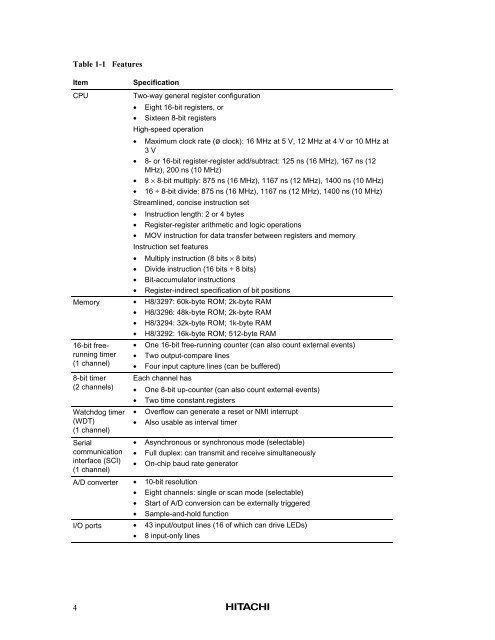
- Page 13: Section 1 Overview1.1 OverviewThe H
- Page 17 and 18: 1.2 Block DiagramFigure 1-1 shows a
- Page 19 and 20: 1.3.2 Pin Functions(1) Pin Assignme
- Page 21 and 22: Table 1-2 Pin Assignments in Each O
- Page 23 and 24: Table 1-3 Pin Functions (cont)TypeS
- Page 25 and 26: Table 1-3 Pin Functions (cont)TypeS
- Page 27: 17605958575655545352515049484746454
- Page 30 and 31: 2.1.2 Address SpaceThe H8/300 CPU s
- Page 32 and 33: 2.2.2 Control RegistersThe CPU cont
- Page 34 and 35: 2.3.1 Data Formats in General Regis
- Page 36 and 37: 2.4 Addressing Modes2.4.1 Addressin
- Page 38 and 39: 2.4.2 Calculation of Effective Addr
- Page 40 and 41: Table 2-2 Effective Address Calcula
- Page 42 and 43: 2.5 Instruction SetThe H8/300 CPU h
- Page 44 and 45: 2.5.1 Data Transfer InstructionsTab
- Page 46 and 47: 2.5.3 Logic OperationsTable 2-6 des
- Page 48 and 49: 2.5.5 Bit ManipulationsTable 2-8 de
- Page 50 and 51: Before Execution of BCLR Instructio
- Page 52 and 53: 2.5.6 Branching InstructionsTable 2
- Page 54 and 55: 2.5.7 System Control InstructionsTa
- Page 56 and 57: Notes on EEPMOV Instruction1. The E
- Page 58 and 59: 2.6.2 Program Execution StateIn thi
- Page 60 and 61: Bus cycleT 1 stateT 2 stateøAddres
- Page 62 and 63: Write cycleT 1 state T 2 state T 3
- Page 64 and 65:
3.2 System Control Register (SYSCR)
- Page 66 and 67:
3.4 Address Space Map in Each Opera
- Page 68 and 69:
58Figure 3-3 H8/3294 Address Space
- Page 71 and 72:
Section 4 Exception Handling4.1 Ove
- Page 73 and 74:
Vector fetchInternalprocessingInstr
- Page 75 and 76:
Table 4-2 InterruptsInterrupt sourc
- Page 77 and 78:
IRQ Enable Register (IER)BitInitial
- Page 79 and 80:
NMI interruptInterrupt controllerCP
- Page 81 and 82:
SP - 4SP - 3SP - 2SP(R7)SP + 1SP +
- Page 83:
CPU writecycle to TIEROCIA interrup
- Page 86 and 87:
5.1.4 Register ConfigurationTable 5
- Page 88 and 89:
Inserted bywait countInserted byWAI
- Page 90 and 91:
Bits 7 and 6—ReservedBit 5—Cloc
- Page 92 and 93:
(2) Input of External Clock Signal1
- Page 94 and 95:
6.3 Duty Adjustment CircuitWhen the
- Page 96 and 97:
Table 7-1 Port FunctionsExpanded Mo
- Page 98 and 99:
7.2.2 Register Configuration and De
- Page 100 and 101:
Mode 2: In mode 2 (expanded mode wi
- Page 102 and 103:
Port 2 pinsPin configurationin mode
- Page 104 and 105:
7.3.3 Pin Functions in Each ModePor
- Page 106 and 107:
Port 4Port 4 pinsP4 7 /WAITP4 6 /ø
- Page 108 and 109:
7.4.3 Pin Functions in Each ModePor
- Page 110 and 111:
7.5 Port 47.5.1 OverviewPort 4 is a
- Page 112 and 113:
7.5.3 Pin FunctionsPort 4 has one s
- Page 114 and 115:
7.6 Port 57.6.1 OverviewPort 5 is a
- Page 116 and 117:
7.7 Port 67.7.1 OverviewPort 6 is a
- Page 118 and 119:
7.7.3 Pin FunctionsPort 6 has the s
- Page 120 and 121:
7.8 Port 77.8.1 OverviewPort 7 is a
- Page 122 and 123:
8.1.2 Block DiagramFigure 8-1 shows
- Page 124 and 125:
Table 8-2 Register Configuration (c
- Page 126 and 127:
Table 8-3 Buffered Input Capture Ed
- Page 128 and 129:
8.2.5 Timer Control/Status Register
- Page 130 and 131:
Bit 1—Timer Overflow Flag (OVF):
- Page 132 and 133:
8.2.7 Timer Output Compare Control
- Page 134 and 135:
(1) Upper byte writeCPU writesdata
- Page 136 and 137:
8.4.2 Output Compare TimingWhen a c
- Page 138 and 139:
(2) Buffered Input Capture Timing:
- Page 140 and 141:
8.4.7 Setting of FRC Overflow Flag
- Page 142 and 143:
(2) Contention between FRC Write an
- Page 144 and 145:
Table 8-5 Effect of Changing Intern
- Page 146 and 147:
Externalclock sourceTMCIInternalclo
- Page 148 and 149:
9.2.2 Time Constant Registers A and
- Page 150 and 151:
Bits 2, 1, and 0—Clock Select (CK
- Page 152 and 153:
Bits 3 to 0—Output Select 3 to 0
- Page 154 and 155:
9.3.2 Compare Match Timing(1) Setti
- Page 156 and 157:
9.4 InterruptsEach channel in the 8
- Page 158 and 159:
9.6.2 Contention between TCNT Write
- Page 160 and 161:
9.6.5 Incrementation Caused by Chan
- Page 162 and 163:
152
- Page 164 and 165:
10.1.3 Register ConfigurationTable
- Page 166 and 167:
Bits 2—0: Clock Select (CKS2-CKS0
- Page 168 and 169:
10.3.2 Interval Timer ModeInterval
- Page 170 and 171:
160
- Page 172 and 173:
11.1.2 Block DiagramFigure 11-1 sho
- Page 174 and 175:
11.2.3 Transmit Shift Register (TSR
- Page 176 and 177:
Bit 2—Multiprocessor Mode (MP): T
- Page 178 and 179:
Bit 3MPIE Description0 The multipro
- Page 180 and 181:
Bit 4—Framing Error (FER): This b
- Page 182 and 183:
Tables 11-3 and 11-4 show examples
- Page 184 and 185:
Table 11-3 Examples of BRR Settings
- Page 186 and 187:
11.2.9 Serial/Timer Control Registe
- Page 188 and 189:
Table 11-6 SCI Clock Source Selecti
- Page 190 and 191:
(2) Clock: In asynchronous mode it
- Page 192 and 193:
• Transmitting Serial Data: Follo
- Page 194 and 195:
• Receiving Serial Data: Follow t
- Page 196 and 197:
(4) Multiprocessor CommunicationThe
- Page 198 and 199:
1StartbitData (ID1)MPBStopbitStartb
- Page 200 and 201:
• Transmitting Serial Data: Follo
- Page 202 and 203:
• Receiving Serial Data: Follow t
- Page 204 and 205:
• Transmitting and Receiving Seri
- Page 206 and 207:
(3) Line Break Detection: When the
- Page 208 and 209:
12.1.2 Block DiagramFigure 12-1 sho
- Page 210 and 211:
12.2 Register Descriptions12.2.1 A/
- Page 212 and 213:
Bits 2 to 0—Channel Select 2 to 0
- Page 214 and 215:
1. Single mode is selected (SCAN =
- Page 216 and 217:
In scan mode, the values given in t
- Page 218 and 219:
208
- Page 220 and 221:
13.1.2 RAM Enable Bit (RAME) in Sys
- Page 222 and 223:
14.2 PROM Mode (H8/3297, H8/3294)14
- Page 224 and 225:
Address in MCU modeH'0000Address in
- Page 226 and 227:
Table 14-6 AC Characteristics(when
- Page 228 and 229:
14.3.3 Reliability of Programmed Da
- Page 230 and 231:
220
- Page 232 and 233:
BitInitial valueRead/Write7SSBY0R/W
- Page 234 and 235:
15.3.3 Clock Settling Time for Exit
- Page 236 and 237:
15.4.3 Timing RelationshipsFigure 1
- Page 238 and 239:
Table 16-2 DC Characteristics (5-V
- Page 240 and 241:
Table 16-3 DC Characteristics (4-V
- Page 242 and 243:
Table 16-4 DC Characteristics (3-V
- Page 244 and 245:
Table 16-5 Allowable Output Current
- Page 246 and 247:
Table 16-7 Bus TimingCondition A:VC
- Page 248 and 249:
Table 16-9 Timing Conditions of On-
- Page 250 and 251:
16.3 MCU Operational TimingThis sec
- Page 252 and 253:
(3) Clock Settling TimingøV CCSTBY
- Page 254 and 255:
(2) SCI Input Clock Timingt SCKWSCK
- Page 256 and 257:
Table A-1 Instruction SetAddressing
- Page 258 and 259:
Table A-1 Instruction Set (cont)Add
- Page 260 and 261:
Table A-1 Instruction Set (cont)Add
- Page 262 and 263:
Table A-1 Instruction Set (cont)Add
- Page 264 and 265:
Table A-2 Operation Code MapLowHigh
- Page 266 and 267:
Table A-4 Number of Cycles in Each
- Page 268 and 269:
Table A-4 Number of Cycles in Each
- Page 270 and 271:
Table A-4 Number of Cycles in Each
- Page 272 and 273:
(Continued from previous page)Bit N
- Page 274 and 275:
(Continued from preceding page)Bit
- Page 276 and 277:
B.2 Function DescriptionsRegister n
- Page 278 and 279:
TCSR—Timer Control/Status Registe
- Page 280 and 281:
TCR—Timer Control RegisterH'FF96
- Page 282 and 283:
ICRA (H and L)—Input Capture Regi
- Page 284 and 285:
TCNT—Timer Counter H’FFA9 (read
- Page 286 and 287:
P4DR—Port 4 Data Register H'FFB7P
- Page 288 and 289:
STCR—Serial/Timer Control Registe
- Page 290 and 291:
MDCR—Mode Control Register H'FFC5
- Page 292 and 293:
TCSR—Timer Control/Status Registe
- Page 294 and 295:
TCR—Timer Control RegisterH'FFD0T
- Page 296 and 297:
SMR—Serial Mode RegisterH'FFD8SCI
- Page 298 and 299:
SCR—Serial Control Register H'FFD
- Page 300 and 301:
SSR—Serial Status Register H'FFDC
- Page 302 and 303:
ADCSR—A/D Control/Status Register
- Page 304 and 305:
294
- Page 306 and 307:
C.2 Port 2 Block DiagramResetHardwa
- Page 308 and 309:
C.4 Port 4 Block DiagramResetRQ DP4
- Page 310 and 311:
Hardware standbyMode 1 or 2ResetRQ
- Page 312 and 313:
WAIT input enableMode 1 or 2ResetRQ
- Page 314 and 315:
P5 2ResetRQ DP5 2 DDRCWP5DResetRQ D
- Page 316 and 317:
ResetRQ DP61 DDRCWP6DResetInternal
- Page 318 and 319:
ResetRQ DP64 DDRCWP6DResetInternal
- Page 320 and 321:
310
- Page 322 and 323:
Table D-1 Port States (cont)Pin Nam
- Page 324 and 325:
314
- Page 326 and 327:
Table F-1 H8/3297 Series Product Co
- Page 328:
Unit: mm17.2 ± 0.31448 33Unit: mm4