Electronic Devices and Amplifier Circuits
Electronic Devices and Amplifier Circuits - Orchard Publications
Electronic Devices and Amplifier Circuits - Orchard Publications

Create successful ePaper yourself
Turn your PDF publications into a flip-book with our unique Google optimized e-Paper software.
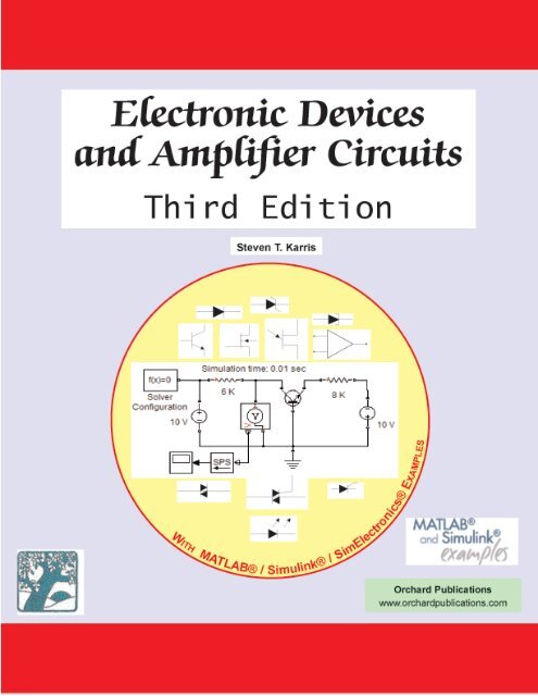
<strong>Electronic</strong> <strong>Devices</strong><strong>and</strong> <strong>Amplifier</strong> <strong>Circuits</strong>with MATLAB® / Simulink® / Sim<strong>Electronic</strong>s® ExamplesThird EditionSteven T. KarrisOrchard Publicationswww.orchardpublications.com
<strong>Electronic</strong> <strong>Devices</strong> <strong>and</strong> <strong>Amplifier</strong> <strong>Circuits</strong> with MATLAB® / Simulink® / Sim<strong>Electronic</strong>s® Examples, Third EditionCopyright ” 2012 Orchard Publications. All rights reserved. Printed in the United States of America. No part of thispublication may be reproduced or distributed in any form or by any means, or stored in a data base or retrieval system,without the prior written permission of the publisher.Direct all inquiries to Orchard Publications, info@orchardpublications.comProduct <strong>and</strong> corporate names are trademarks or registered trademarks of The MathWorks, Inc. They are used only foridentification <strong>and</strong> explanation, without intent to infringe.Library of Congress Cataloging−in−Publication DataLibrary of Congress Control Number (LCCN) : 2012943157TXu1−254-969ISBN-13: 978−1−934404−25−6ISBN-10: 1−934404−25−XDisclaimerThe author has made every effort to make this text as complete <strong>and</strong> accurate as possible, but no warranty is implied.The author <strong>and</strong> publisher shall have neither liability nor responsibility to any person or entity with respect to any loss ordamages arising from the information contained in this text.
PrefaceThis text is an undergraduate level textbook presenting a thorough discussion of state−of−the artelectronic devices. It is self−contained; it begins with an introduction to solid state semiconductordevices. The prerequisites for this text are first year calculus <strong>and</strong> physics, <strong>and</strong> a two−semester coursein circuit analysis including the fundamental theorems <strong>and</strong> the Laplace transformation. Noprevious knowledge of MATLAB® is required; the material in Appendix A <strong>and</strong> the inexpensiveMATLAB Student Version is all the reader needs to get going. The discussions are based on a PCwith the Windows 7 platform but if you have another platform such as Macintosh, please refer tothe appropriate sections of the MATLAB’s User Guide which also contains instructions forinstallation. Additional information including purchasing may be obtained from The MathWorks,Inc., 3 Apple Hill Drive, Natick, MA 01760-2098. Phone: 508 647−7000, Fax: 508 647−7001, e−mail: info@mathwork.com <strong>and</strong> web site http://www.mathworks.com. Even though this text canalso be used without MATLAB, it is highly recommended to be used with the inexpensiveMATLAB Student Version. The MATLAB scripts in this text are available free of charge uponrequest. Contact us at info@orchardpublications.com.This is our fourth electrical <strong>and</strong> computer engineering-based text with MATLAB applications. Myassociates, contributors, <strong>and</strong> I have a mission to produce substance <strong>and</strong> yet inexpensive texts for theaverage reader. Our first three texts * are very popular with students <strong>and</strong> working professionalsseeking to enhance their knowledge <strong>and</strong> prepare for the professional engineering examination.The author <strong>and</strong> contributors make no claim to originality of content or of treatment, but havetaken care to present definitions, statements of physical laws, theorems, <strong>and</strong> problems.Chapter 1 is an introduction to the nature of small signals used in electronic devices, amplifiers,definitions of decibels, b<strong>and</strong>width, poles <strong>and</strong> zeros, stability, transfer functions, <strong>and</strong> Bode plots.Chapter 2 is an introduction to solid state electronics beginning with simple explanations ofelectron <strong>and</strong> hole movement. This chapter provides a thorough discussion on the junction diode<strong>and</strong> its volt-ampere characteristics. In most cases, the non−linear characteristics are plotted withsimple MATLAB scripts. The discussion concludes with diode applications, the Zener, Schottky,tunnel, <strong>and</strong> varactor diodes, <strong>and</strong> optoelectronics devices. Chapters 3 <strong>and</strong> 4 are devoted to bipolarjunction transistors <strong>and</strong> FETs respectively, <strong>and</strong> many examples with detailed solutions are provided.Chapter 5 is a long chapter on op amps. Many op amp circuits are presented <strong>and</strong> their applicationsare well illustrated.* These are Circuit Analysis I with MATLAB® Computing <strong>and</strong> Simulink®/SimPowerSystems® Modeling, ISBN978−1−934404−17−1, Circuit Analysis II with MATLAB® Computing <strong>and</strong> Simulink®/SimPowerSystems®Modeling, ISBN 978−1−934404−19−5, <strong>and</strong> Signals <strong>and</strong> Systems with MATLAB® Computing <strong>and</strong> Simulink®Modeling, ISBN 978−1−934404−23−2.
The highlight of this text is Chapter 6 on integrated devices used in logic circuits. The internalconstruction <strong>and</strong> operation of the TTL, NMOS, PMOS, CMOS, ECL, <strong>and</strong> the biCMOS familiesof those devices are fully discussed. Moreover, the interpretation of the most important parameterslisted in the manufacturers data sheets are explained in detail. Chapter 7 is an introduction to pulsecircuits <strong>and</strong> waveform generators. There, the 555 Timer, the astable, monostable, <strong>and</strong> bistablemultivibrators, <strong>and</strong> the Schmitt trigger are discussedChapter 8 discusses to the frequency characteristic of single-stage <strong>and</strong> cascade amplifiers, <strong>and</strong>Chapter 9 is devoted to tuned amplifiers. Sinusoidal oscillators are introduced in Chapter 10.This is the third edition of this title, <strong>and</strong> includes several Simulink, SimPowerSystems, <strong>and</strong>Sim<strong>Electronic</strong>s models. Appendix A, is an introduction to MATLAB®. Appendix B is anintroduction to Simulink, Appendix C is an introduction to Simscape® toolbox that includesSimPowerSystems® <strong>and</strong> Sim<strong>Electronic</strong>s® libraries, Appendix D is an introduction to Proportional-Integral-Derivative (PID) controllers, Appendix E describes uncompensated <strong>and</strong> compensatednetworks, <strong>and</strong> Appendix F discusses the substitution, reduction, <strong>and</strong> Miller’s theorems.The author wishes to express his gratitude to the staff of The MathWorks, the developers ofMATLAB® <strong>and</strong> Simulink® for the encouragement <strong>and</strong> unlimited support they have provided mewith during the production of this text.A companion to this text, Digital Circuit Analysis <strong>and</strong> Design with Simulink® Modeling <strong>and</strong> Introductionto CPLDs <strong>and</strong> FPGAs, ISBN 978−1−934404−05−8 is recommended as a companion. This text isdevoted strictly on Boolean logic, combinational <strong>and</strong> sequential circuits as interconnected logicgates <strong>and</strong> flip−flops, an introduction to static <strong>and</strong> dynamic memory devices. <strong>and</strong> other relatedtopics.Although every effort was made to correct possible typographical errors <strong>and</strong> erroneous references tofigures <strong>and</strong> tables, some may have been overlooked. Our experience is that the best proofreader isthe reader. Accordingly, the author will appreciate it very much if any such errors are brought to hisattention so that corrections can be made for the next edition. We will be grateful to readers whodirect these to our attention at info@orchardpublications.com. Thank you.Orchard PublicationsFremont, California 94538−4741United States of Americawww.orchardpublications.cominfo@orchardpublications.com
Table of Contents1 Basic <strong>Electronic</strong> Concepts <strong>and</strong> Signals1.1 Signals <strong>and</strong> Signal Classifications ........................................................................... 1−11.2 <strong>Amplifier</strong>s................................................................................................................ 1−31.3 Decibels ................................................................................................................... 1−31.4 B<strong>and</strong>width <strong>and</strong> Frequency Response...................................................................... 1−51.5 Bode Plots............................................................................................................... 1−71.6 Transfer Function ................................................................................................... 1−91.7 Poles <strong>and</strong> Zeros...................................................................................................... 1−101.8 Stability.................................................................................................................. 1−111.9 Voltage <strong>Amplifier</strong> Equivalent Circuit................................................................... 1−151.10 Current <strong>Amplifier</strong> Equivalent Circuit.................................................................. 1−171.11 Summary................................................................................................................ 1−191.12 Exercises ................................................................................................................ 1−221.13 Solutions to End−of−Chapter Exercises............................................................... 1−24MATLAB ScriptsPages 1−7, 1−13, 1−14, 1−16, 1−25, 1−26, 1−27, 1−29, 1−30Simulink/SimPowerSystems/Sim<strong>Electronic</strong>s ModelsPages 1−32, 1−332 Introduction to Semiconductor <strong>Electronic</strong>s − Diodes2.1 Electrons <strong>and</strong> Holes..................................................................................................2−12.2 Junction Diode.........................................................................................................2−42.3 Graphical Analysis of <strong>Circuits</strong> with Non−Linear <strong>Devices</strong>........................................2−82.4 Piecewise Linear Approximations..........................................................................2−122.5 Low Frequency AC <strong>Circuits</strong> with Junction Diodes...............................................2−152.6 Junction Diode Applications in AC <strong>Circuits</strong> ........................................................2−182.7 Peak Rectifier <strong>Circuits</strong> ...........................................................................................2−302.8 Clipper <strong>Circuits</strong>......................................................................................................2−312.9 DC Restorer <strong>Circuits</strong> .............................................................................................2−342.10 Voltage Doubler <strong>Circuits</strong> .......................................................................................2−352.11 Diode Applications in Amplitude Modulation (AM) Detection <strong>Circuits</strong> ............2−352.12 Diode Applications in Frequency Modulation (FM) Detection <strong>Circuits</strong>..............2−362.13 Zener Diodes ..........................................................................................................2−372.14 Schottky Diode.......................................................................................................2−432.15 Tunnel Diode.........................................................................................................2−442.16 Varactor................................................................................................................. 2−462.17 Optoelectronic <strong>Devices</strong> ......................................................................................... 2−462.18 Summary................................................................................................................ 2−50<strong>Electronic</strong> <strong>Devices</strong> <strong>and</strong> <strong>Amplifier</strong> <strong>Circuits</strong> with MATLAB® / Simulink® / Sim<strong>Electronic</strong>s® Examples, Third EditionCopyright © Orchard Publicationsi
2.19 Exercises.................................................................................................................2−542.20 Solutions to End−of−Chapter Exercises ...............................................................2−59MATLAB ScriptsPages 2−6, 2−27, 2−28, 2−59, 2−67Simulink/SimPowerSystems/Sim<strong>Electronic</strong>s ModelsPages 2−14, 2−18, 2−23, 2−24, 2−29, 2−43, 2−613 Bipolar Junction Transistors3.1 Introduction ..........................................................................................................3−13.2 NPN Transistor Operation....................................................................................3−33.3 Bipolar Junction Transistor as an <strong>Amplifier</strong> .........................................................3−33.3.1 Equivalent Circuit Models − NPN Transistors...........................................3−63.3.2 Equivalent Circuit Models − PNP Transistors...........................................3−73.3.3 Effect of Temperature on the i C – v BE − Characteristics...........................3−93.3.4 Collector Output Resistance − Early Voltage ..........................................3−103.4 Transistor <strong>Amplifier</strong> Circuit Biasing...................................................................3−183.5 Fixed Bias.............................................................................................................3−203.6 Self−Bias ..............................................................................................................3−253.7 <strong>Amplifier</strong> Classes <strong>and</strong> Operation........................................................................3−273.7.1 Class A <strong>Amplifier</strong> Operation ...................................................................3−303.7.2 Class B <strong>Amplifier</strong> Operation....................................................................3−333.7.3 Class AB <strong>Amplifier</strong> Operation.................................................................3−353.7.4 Class C <strong>Amplifier</strong> Operation ...................................................................3−373.8 Graphical Analysis...............................................................................................3−383.9 Power Relations in the Basic Transistor <strong>Amplifier</strong> .............................................3−423.10 Piecewise−Linear Analysis of the Transistor <strong>Amplifier</strong>.......................................3−433.11 Incremental Linear Models .................................................................................3−483.12 Transconductance ...............................................................................................3−533.13 High−Frequency Models for Transistors.............................................................3−543.14 The Darlington Connection ...............................................................................3−583.15 Transistor Networks.............................................................................................3−593.15.1 h−Equivalent Circuit for the Common−Base Transistor.......................3−593.15.2 T−Equivalent Circuit for the Common−Base Transistor.......................3−633.15.3 h−Equivalent Circuit for the Common−Emitter Transistor..................3−643.15.4 T−Equivalent Circuit for the Common−Emitter Transistor..................3−683.15.5 h−Equivalent Circuit for the Common−Collector Transistor...............3−693.15.6 T−Equivalent Circuit for the Common−Collector Transistor...............3−753.16 Transistor Cutoff <strong>and</strong> Saturation Regions .......................................................... 3−763.16.1 Cutoff Region ........................................................................................3−763.16.2 Active Region .........................................................................................3−763.16.3 Saturation Region ..................................................................................3−77ii<strong>Electronic</strong> <strong>Devices</strong> <strong>and</strong> <strong>Amplifier</strong> <strong>Circuits</strong> with MATLAB® / Simulink® / Sim<strong>Electronic</strong>s® Examples, Third EditionCopyright © Orchard Publications
3.17 The Ebers−Moll Transistor Model......................................................................3−793.18 Schottky Diode Clamp........................................................................................3−833.19 Transistor Specifications.................................................................................... 3−833.20 Summary ............................................................................................................ 3−853.21 Exercises ............................................................................................................. 3−893.22 Solutions to End−of−Chapter Exercises.............................................................3−95MATLAB ScriptsPages 3−12, 3−38, 3−111Simulink/SimPowerSystems/Sim<strong>Electronic</strong>s ModelPage 3−994 Field Effect Transistors <strong>and</strong> PNPN <strong>Devices</strong>4.1 Junction Field Effect Transistor (JFET) ................................................................4−14.2 Metal Oxide Semiconductor Field Effect Transistor (MOSFET)..................... 4−64.2.1 N−Channel MOSFET in the Enhancement Mode................................... 4−74.2.2 N−Channel MOSFET in the Depletion Mode ...................................... 4−124.2.3 P−Channel MOSFET in the Enhancement Mode ................................. 4−154.2.4 P−Channel MOSFET in the Depletion Mode ....................................... 4−184.2.5 Voltage Gain ......................................................................................... 4−184.3 Complementary MOS (CMOS)....................................................................... 4−204.3.1 CMOS Common−Source <strong>Amplifier</strong> ..................................................... 4−204.3.2 CMOS Common−Gate <strong>Amplifier</strong>......................................................... 4−214.3.3 CMOS Common−Drain (Source Follower) <strong>Amplifier</strong>......................... 4−214.4 Metal Semiconductor FET (MESFET)............................................................ 4−224.5 Unijunction Transistor..................................................................................... 4−234.6 Diac.................................................................................................................. 4−244.7 Silicon Controlled Rectifier (SCR).................................................................. 4−244.7.1 SCR as an <strong>Electronic</strong> Switch ................................................................ 4−274.7.2 SCR in the Generation of Sawtooth Waveforms .................................. 4−284.8 Triac ............................................................................................................... 4−394.9 Shockley Diode.............................................................................................. 4−404.10 Other PNPN <strong>Devices</strong>...................................................................................... 4−414.11 The Future of Transistors............................................................................... 4−424.12 Summary........................................................................................................ 4−444.13 Exercises ........................................................................................................ 4−474.14 Solutions to End−of−Chapter Exercises ........................................................ 4−49MATLAB ScriptsPages 4−5, 4−9Simulink/SimPowerSystems/Sim<strong>Electronic</strong>s ModelsPages 4−11, 4−17, 4−37, 4−38<strong>Electronic</strong> <strong>Devices</strong> <strong>and</strong> <strong>Amplifier</strong> <strong>Circuits</strong> with MATLAB® / Simulink® / Sim<strong>Electronic</strong>s® Examples, Third EditionCopyright © Orchard Publicationsiii
5 Operational <strong>Amplifier</strong>s5.1 Operational <strong>Amplifier</strong> ........................................................................................5−15.2 An Overview of the Op Amp .............................................................................5−15.3 Op Amp in the Inverting Mode .........................................................................5−25.4 Op Amp in the Non−Inverting Mode................................................................5−55.5 Active Filters........................................................................................................5−85.6 Analysis of Op Amp <strong>Circuits</strong>............................................................................5−115.7 Input <strong>and</strong> Output Resistances..........................................................................5−215.8 Op Amp Open Loop Gain ...............................................................................5−245.9 Op Amp Closed Loop Gain .............................................................................5−265.10 Transresistance <strong>Amplifier</strong> .................................................................................5−285.11 Closed Loop Transfer Function .......................................................................5−295.12 Op Amp Integrator ...........................................................................................5−305.13 Op Amp Differentiator .....................................................................................5−345.14 Summing <strong>and</strong> Averaging Op Amp <strong>Circuits</strong>5−375.15 Differential Input Op Amp...............................................................................5−385.16 Instrumentation <strong>Amplifier</strong>s...............................................................................5−415.17 Offset Nulling....................................................................................................5−435.18 External Frequency Compensation...................................................................5−435.19 Slew Rate ...........................................................................................................5−445.20 <strong>Circuits</strong> with Op Amps <strong>and</strong> Non-Linear <strong>Devices</strong> .............................................5−455.21 Comparator .......................................................................................................5−485.22 Wien Bridge Oscillator......................................................................................5−495.23 Digital−to−Analog Converters ..........................................................................5−515.24 Analog−to−Digital Converters ..........................................................................5−565.24.1 Flash Analog−to−Digital Converter ......................................................5−555.24.2 Successive Approximation Analog−to−Digital Converter ....................5−575.24.3 Dual−Slope Analog−to−Digital Converter............................................5−585.25 Quantization, Quantization Error, Accuracy, <strong>and</strong> Resolution ........................5−605.26 Op Amps in Analog Computers .....................................................................5−625.27 Gyrator..............................................................................................................5−655.28 Summary ...........................................................................................................5−695.29 Exercises............................................................................................................5−735.30 Solutions to End−of−Chapter Exercises...........................................................5−80MATLAB ScriptsPages 5−82, 5−90Simulink/SimPowerSystems/Sim<strong>Electronic</strong>s ModelsPages 5−5, 5−34, 5−68iv<strong>Electronic</strong> <strong>Devices</strong> <strong>and</strong> <strong>Amplifier</strong> <strong>Circuits</strong> with MATLAB® / Simulink® / Sim<strong>Electronic</strong>s® Examples, Third EditionCopyright © Orchard Publications
6 Integrated <strong>Circuits</strong>6.1 Basic Logic Gates................................................................................................. 6−16.2 Positive <strong>and</strong> Negative Logic ................................................................................ 6−16.3 Inverter................................................................................................................ 6−26.4 AND Gate........................................................................................................... 6−66.5 OR Gate.............................................................................................................. 6−86.6 NAND Gate........................................................................................................ 6−96.7 NOR Gate......................................................................................................... 6−136.8 Exclusive OR (XOR) <strong>and</strong> Exclusive NOR (XNOR) Gates............................... 6−156.9 Fan−In, Fan−Out, TTL Unit Load, Sourcing Current, <strong>and</strong> Sinking Current 6−176.10 Data Sheets ....................................................................................................... 6−206.11 Emitter Coupled Logic (ECL) .......................................................................... 6−246.12 NMOS Logic Gates........................................................................................... 6−286.12.1 NMOS Inverter..................................................................................... 6−306.12.2 NMOS NAND Gate ............................................................................. 6−316.12.3 NMOS NOR Gate................................................................................ 6−326.13 CMOS Logic Gates .......................................................................................... 6−326.13.1 CMOS Inverter ..................................................................................... 6−336.13.2 CMOS NAND Gate ............................................................................. 6−346.13.3 CMOS NOR Gate..................................................................................6−346.14 Buffers, Tri-State <strong>Devices</strong>, <strong>and</strong> Data Buses .......................................................6−356.15 Present <strong>and</strong> Future Technologies......................................................................6−396.16 Summary............................................................................................................6−436.17 Exercises.............................................................................................................6−4676.18 Solutions to End−of−Chapter Exercises ...........................................................6−49Pulse <strong>Circuits</strong> <strong>and</strong> Waveform Generators7.1 Astable (Free-Running) Multivibrators.................................................................7−17.2 555 Timer .............................................................................................................7−27.3 Astable Multivibrator with 555 Timer .................................................................7−37.4 Monostable Multivibrators .................................................................................7−157.5 Bistable Multivibrators (Flip−Flops) ...................................................................7−217.5.1 Fixed−Bias Flip-Flop...............................................................................7−217.5.2 Self−Bias Flip−Flop ................................................................................7−247.5.3 Triggering Signals for Flip−Flops ...........................................................7−297.5.4 Present Technology Bistable Multivibrators ..........................................7−317.6 Schmitt Trigger..................................................................................................7−327.7 Summary............................................................................................................7−357.8 Exercises.............................................................................................................7−367.9 Solutions to End−of−Chapter Exercises ...........................................................7−39MATLAB ScriptsPages 7−10, 7−28, 7−40, 7−41<strong>Electronic</strong> <strong>Devices</strong> <strong>and</strong> <strong>Amplifier</strong> <strong>Circuits</strong> with MATLAB® / Simulink® / Sim<strong>Electronic</strong>s® Examples, Third EditionCopyright © Orchard Publicationsv
Simulink/SimPowerSystems/Sim<strong>Electronic</strong>s ModelsPages 7−14, 7−208 Frequency Characteristics of Single−Stage <strong>and</strong> Cascaded <strong>Amplifier</strong>s8.1 Properties of Signal Waveforms............................................................................8−18.2 Transistor <strong>Amplifier</strong> at Low Frequencies .............................................................8−58.3 Transistor <strong>Amplifier</strong> at High Frequencies............................................................8−98.4 Combined Low- <strong>and</strong> High−Frequency Characteristics ......................................8−148.5 Frequency Characteristics of Cascaded <strong>Amplifier</strong>s ............................................8−148.6 Overall Characteristics of Multistage <strong>Amplifier</strong>s................................................8−258.7 Amplification <strong>and</strong> Power Gain in Three or More Cascaded <strong>Amplifier</strong>s...........8−308.8 Summary .............................................................................................................8−328.9 Exercises ..............................................................................................................8−348.10 Solutions to End−of−Chapter Exercises.............................................................8−37MATLAB ScriptsPages 8−8, 8−23, 8−439 Tuned <strong>Amplifier</strong>s9.1 Introduction to Tuned <strong>Circuits</strong> ............................................................................ 9−19.2 Single-tuned Transistor <strong>Amplifier</strong>......................................................................... 9−89.3 Cascaded Tuned <strong>Amplifier</strong>s................................................................................ 9−139.3.1 Synchronously Tuned <strong>Amplifier</strong>s............................................................. 9−149.3.2 Stagger−Tuned <strong>Amplifier</strong>s ....................................................................... 9−179.3.3 Three or More Tuned <strong>Amplifier</strong>s Connected in Cascade....................... 9−269.4 Summary .............................................................................................................. 9−279.5 Exercises............................................................................................................... 9−299.6 Solutions to End−of−Chapter Exercises.............................................................. 9−30MATLAB ScriptPage 9−1710 Sinusoidal Oscillators10.1 Oscillators Defined.............................................................................................10−110.2 Sinusoidal Oscillators.........................................................................................10−110.3 RC Oscillator......................................................................................................10−410.4 LC Oscillator......................................................................................................10−510.5 Armstrong Oscillator..........................................................................................10−610.6 Hartley Oscillator ...............................................................................................10−710.7 Colpitts Oscillator ..............................................................................................10−710.8 Crystal Oscillators ..............................................................................................10−810.9 Pierce Oscillator ...............................................................................................10−1010.10 Summary...........................................................................................................10−12vi<strong>Electronic</strong> <strong>Devices</strong> <strong>and</strong> <strong>Amplifier</strong> <strong>Circuits</strong> with MATLAB® / Simulink® / Sim<strong>Electronic</strong>s® Examples, Third EditionCopyright © Orchard Publications
A10.11 Exercises ........................................................................................................... 10−1410.12 Solutions to End−of−Chapter Exercises ......................................................... 10−15Introduction to MATLAB®A.1 MATLAB® <strong>and</strong> Simulink®................................................................................A−1A.2 Comm<strong>and</strong> Window.............................................................................................A−1A.3 Roots of Polynomials...........................................................................................A−3A.4 Polynomial Construction from Known Roots....................................................A−4A.5 Evaluation of a Polynomial at Specified Values..................................................A−6A.6 Rational Polynomials...........................................................................................A−8A.7 Using MATLAB to Make Plots .........................................................................A−10A.8 Subplots .............................................................................................................A−18A.9 Multiplication, Division <strong>and</strong> Exponentiation...................................................A−18A.10 Script <strong>and</strong> Function Files ..................................................................................A−26A.11 Display Formats .................................................................................................A−31MATLAB ScriptsPages A−3 through A−9, A−11 through A−13, A−16,A−17 through A−21, A−23, A−24, A−26, A−27B Introduction to Simulink®B.1 Simulink <strong>and</strong> its Relation to MATLAB................................................................B−1B.2 Simulink Demos .................................................................................................B−20MATLAB ScriptPage B−4CSimulink/SimPowerSystems/Sim<strong>Electronic</strong>s ModelsPages B−12, B−17, B−19Introduction to Simscape®C.1 Simscape Libraries................................................................................................ C−1C.1.1 Foundation Library ....................................................................................C−1C.1.2 Utilities Library..........................................................................................C−3C.1.3 Sim<strong>Electronic</strong>s Library...............................................................................C−4C.1.4 SimPowerSystems Library ..........................................................................C−7Simulink/SimPowerSystems/Sim<strong>Electronic</strong>s ModelPage C−4D Proportional−Integral−Derivative (PID) ControllerD.1 Description <strong>and</strong> Components of a Typical PID.................................................. D−1D.2 The Simulink PID Blocks .................................................................................... D−2Simulink/SimPowerSystems/Sim<strong>Electronic</strong>s ModelsPages D−3, D−4<strong>Electronic</strong> <strong>Devices</strong> <strong>and</strong> <strong>Amplifier</strong> <strong>Circuits</strong> with MATLAB® / Simulink® / Sim<strong>Electronic</strong>s® Examples, Third EditionCopyright © Orchard Publicationsvii
EFCompensated AttenuatorsE.1 Uncompensated Attenuator .................................................................................E−1E.2 Compensated Attenuator......................................................................................E−2Substitution, Reduction, <strong>and</strong> Miller’s TheoremsF.1 Substitution Theorem............................................................................................ F−1F.2 Reduction Theorem............................................................................................... F−6F.3 Miller’s Theorem................................................................................................. F−10ReferencesIndexR−1IN−1viii<strong>Electronic</strong> <strong>Devices</strong> <strong>and</strong> <strong>Amplifier</strong> <strong>Circuits</strong> with MATLAB® / Simulink® / Sim<strong>Electronic</strong>s® Examples, Third EditionCopyright © Orchard Publications
1.4 B<strong>and</strong>width <strong>and</strong> Frequency ResponseB<strong>and</strong>width <strong>and</strong> Frequency ResponseLike electric filters, amplifiers exhibit a b<strong>and</strong> of frequencies over which the output remains nearlyconstant. Consider, for example, the magnitude of the output voltage V outof an electric or electroniccircuit as a function of radian frequency ω as shown in Figure 1.5.As shown in Figure 1.5, the b<strong>and</strong>width is BW = ω 2 – ω 1where ω 1<strong>and</strong> ω 2are the cutoff frequencies.At these frequencies, V out = 2 ⁄ 2 = 0.707 <strong>and</strong> these two points are known as the 3−dB down orhalf−power points. They derive their name from the fact that since power p = v 2 ⁄ R = i 2 ⋅ R , forR = 1 <strong>and</strong> for v or i = 2⁄ 2 = 0.707 the power is 1 ⁄ 2, that is, it is “halved”.1V out0.707B<strong>and</strong>widthωω 1ω 2Figure 1.5. Definition of b<strong>and</strong>widthAlternately, we can define the b<strong>and</strong>width as the frequency b<strong>and</strong> between half−power points. Werecall from the characteristics of electric filters, the low−pass <strong>and</strong> high−pass filters have only one cutofffrequency whereas b<strong>and</strong>−pass <strong>and</strong> b<strong>and</strong>−elimination (b<strong>and</strong>−stop) filters have two. We may thinkthat low−pass <strong>and</strong> high−pass filters have also two cutoff frequencies where in the case of the low−pass filter the second cutoff frequency is at ω = 0 while in a high−pass filter it is at ω = ∞.We also recall also that the output of circuit is dependent upon the frequency when the input is asinusoidal voltage. In general form, the output voltage is expressed asV out ( ω) = V out ( ω) e jϕω ( )(1.12)where V out ( ω) is known as the magnitude response <strong>and</strong> e jϕω is known as the phase response. Thesetwo responses together constitute the frequency response of a circuit.( )RCExample 1.1Derive <strong>and</strong> sketch the magnitude <strong>and</strong> phase responses of the1.6.low−pass filter shown in Figurev inRCv outFigure 1.6. RC low−pass filter<strong>Electronic</strong> <strong>Devices</strong> <strong>and</strong> <strong>Amplifier</strong> <strong>Circuits</strong> with MATLAB® / Simulink® / Sim<strong>Electronic</strong>s® Examples, Third EditionCopyright © Orchard Publications1−5
Chapter 1 Basic <strong>Electronic</strong> Concepts <strong>and</strong> SignalsFrom Figure 1.16 we observe that all poles, denoted as , lie on the left−h<strong>and</strong> half−plane <strong>and</strong>thus the system is stable. The location of the zeros, denoted as , is immaterial.b. We use the MATLAB exp<strong>and</strong>(s) symbolic function to express the numerator <strong>and</strong> denominatorof Gs ( ) in polynomial formsyms s; n=exp<strong>and</strong>((s−1)*(s^2+2*s+5)), d=exp<strong>and</strong>((s+2)*(s^2+6*s+25))n = s^3+s^2+3*s-5d = s^3+s^2+3*s-5<strong>and</strong> thusGs ( )For this example we are interested in the magnitude only so we will use the scriptnum=3*[1 1 3 −5]; den=[1 8 37 50]; sys=tf(num,den);...w=logspace(0,2,100); bodemag(sys,w); gridThe magnitude plot is shown in Figure 1.17.3s ( 3 + s 2 + 3s – 5)= --------------------------------------------------( s 3 + 8s 2 + 37s + 50)Frequency (rad/sec, log scale)Figure 1.17. Bode plot for Example 1.3Example 1.4It is known that a voltage amplifier has a frequency response of a low−pass filter, a DC gain of80 dB , attenuation of – 20 dB per decade, <strong>and</strong> the 3 dB cutoff frequency occurs at 10 KHz.Determine the gain (in dB) at the frequencies 1 KHz, 10 KHz , 100KHz , 1 MHz, 10 MHz , <strong>and</strong>100 MHz .Solution:Using the given data we construct the asymptotic magnitude response shown in Figure 1.18 fromwhich we obtain the data shown on the table below.1−14<strong>Electronic</strong> <strong>Devices</strong> <strong>and</strong> <strong>Amplifier</strong> <strong>Circuits</strong> with MATLAB® / Simulink® / Sim<strong>Electronic</strong>s® Examples, Third EditionCopyright © Orchard Publicationss
Chapter 1 Basic <strong>Electronic</strong> Concepts <strong>and</strong> Signals1.12 Exercises1. Following the procedure of Example 1.1, derive <strong>and</strong> sketch the magnitude <strong>and</strong> phase responsesfor an RC high−pass filter.2. Derive the transfer function Gs ( ) for the network shown below.+v in () t−CL0.5 H+ − +1 FR1 Ωv out () t−3. A system has poles at – 4 , – 2 + j, – 2 – j, <strong>and</strong> zeros at – 1 , – 3 + j2, <strong>and</strong> – 3 – j2. Derive thetransfer function of this system given that G( ∞) = 10 .4. The circuit model shown below is known as a transresistance amplifier <strong>and</strong> the ideal characteristicsfor this amplifier are R in → 0 <strong>and</strong> R out → 0 .i inR outv ini outv outv outR R in in = ---------iR in i inini out= 0With a voltage source in series with resistance connected on the input side <strong>and</strong> a loadv sresistance connected to the output, the circuit is as shown below.R sR load+v S2cosωt mV+−R Si in1 KΩ + v in−R in C−10 KΩ 0.1 nFR out100 Ω R loadR m i m5 KΩ+v load−Find the overall voltage gain A v = v load ⁄ v sif R m = 100 Ω . Then, use MATLAB to plot themagnitude of A vfor the range 10 3 ≤ω ≤10 8 . From the plot, estimate the 3 dB cutoff frequency.1−22<strong>Electronic</strong> <strong>Devices</strong> <strong>and</strong> <strong>Amplifier</strong> <strong>Circuits</strong> with MATLAB® / Simulink® / Sim<strong>Electronic</strong>s® Examples, Third EditionCopyright © Orchard Publicationss
Chapter 1 Basic <strong>Electronic</strong> Concepts <strong>and</strong> Signals4.The s – domainequivalent circuit is shown below.V S ( s)+−I in ( s)+10 3V in ( s)10 4−+−10 10 ⁄ s+−10 2100I in ( s) 5 × 10 3+V load ( s)−The parallel combination of the 10 4 resistor <strong>and</strong> 10 10 ⁄ s capacitor yields<strong>and</strong> by the voltage division expressionZs ( ) 10 4 10 10 10 14 ⁄ s= || ⁄ s = ----------------------------------10 4 + 10 10 =⁄ s10 14------------------------------10 4 s + 10 10Also,whereV in ( s)V load ( s)10 14 ⁄ ( 10 4 s + 10 10 )10 14= -------------------------------------------------------------V10 3 + 10 14 ⁄ ( 10 4 s + 10 10 S ( s)= -----------------------------------------V () 10 7 14s ) Ss + 1.1×105 × 10 35 × 10 5= -------------------------------100I10 2 + 5 × 10 3 in ( s)= ---------------------I3 in ( s) = 98I in ( s)5.1 × 10(1)1−28<strong>Electronic</strong> <strong>Devices</strong> <strong>and</strong> <strong>Amplifier</strong> <strong>Circuits</strong> with MATLAB® / Simulink® / Sim<strong>Electronic</strong>s® Examples, Third EditionCopyright © Orchard Publicationss
The Junction DiodeFigure 2.12. Voltage−current characteristics of a forward−biased junction diode.The curve in Figure 2.12 shows that in a junction diode made with silicon <strong>and</strong> an impurity, conventionalcurrent will flow in the direction of the arrow of the diode as long as the voltage drop v Dacross the diode is about 0.65 volt or greater. We also observe that at v D = 0.7 V , the currentthrough the diode is ≈ 0.5 mA .When a junction diode is reverse−biased, as shown in Figure 2.13, a very small current will flow <strong>and</strong>if the applied voltage exceeds a certain value the diode will reach its avalanche or Zener region. Thevoltage−current characteristics of a reverse biased junction diode are shown in Figure 2.13 whereis referred to as the Zener diode voltage. Zener diodes are discussed in the next section.V Zi DAvalanche RegionV Z0ivFigure 2.13. The reverse biased region of a junction diodeCommercially available diodes are provided with a given rating (volts, watts) by the manufacturer,<strong>and</strong> if these ratings are exceeded, the diode will burn−out in either the forward−biased or thereverse−biased direction.The maximum amount of average current that can be permitted to flow in the forward direction isreferred to as the maximum average forward current <strong>and</strong> it is specified at a special temperature, usually25 °C . If this rating is exceeded, structure breakdown can occur.The maximum peak current that can be permitted to flow in the forward direction in the form ofrecurring pulses is referred to as the peak forward current.<strong>Electronic</strong> <strong>Devices</strong> <strong>and</strong> <strong>Amplifier</strong> <strong>Circuits</strong> with MATLAB® / Simulink® / Sim<strong>Electronic</strong>s® Examples, Third EditionCopyright © Orchard Publications2−7
Chapter 2 Introduction to Semiconductor <strong>Electronic</strong>s − DiodesFigure 2.23. Model for Example 2.4 with SimPowerSystems blocksI 1 I 220 Ω 20 Ω 20 Ω0.3 V 1.3 V 2.3 VI 3I 41 KΩV outFigure 2.24. Piecewise linear equivalent circuit for Example 2.415 – 50V out + 65– 50V out + 115 – 50V out – V------------------------------------------------------------------------------------------------------------------------- out= 01000This value is not consistent with the value displayed in the model in Figure 2.23, so we perform thefollowing check:I 1 ≈( 0.3 – 1.3) ⁄ 20 ≈ – 50 mAI 2 ≈ ( 1.3 – 1.3) ⁄ 20 ≈ 0I 3 = ( 2.3 – 1.3) ⁄ 20 ≈ 50 mAI 4 = 1.3 ⁄ 1000 = 1.3 mAI 1 + I 2 + I 3 ≠ I 42−14<strong>Electronic</strong> <strong>Devices</strong> <strong>and</strong> <strong>Amplifier</strong> <strong>Circuits</strong> with MATLAB® / Simulink® / Sim<strong>Electronic</strong>s® Examples, Third EditionCopyright © Orchard Publications
The minus (−) sign for the currentI 1Low Frequency AC <strong>Circuits</strong> with Junction Diodesindicates that this current flows in the opposite direction ofthe one shown. Also, the current is zero. Therefore, we must conclude that only the diode on theright side conducts <strong>and</strong> by the voltage division expressionI 2V out1000=----------------------- × 2.3 ≈ 2.3 V20 + 10002.5 Low Frequency AC <strong>Circuits</strong> with Junction DiodesWhen used with AC circuits of low frequencies, diodes, usually with 1.8 ≤n ≤2.0are biased tooperate at some point in the neighborhood of the relatively linear region of the i – v characteristicswhere 0.65 ≤v D ≤ 0.8 V . A bias point denoted as Q whose coordinates are QV ( D , I D ) is shown inFigure 2.25 for a junction diode with n = 2.Qi D () ttv D () tFigure 2.25. Junction diode biased at point Q <strong>and</strong> changes inFigure 2.25 shows how changes in v D () t result in changes in i D () t .i Dtcorresponding to changes inv D<strong>Electronic</strong> <strong>Devices</strong> <strong>and</strong> <strong>Amplifier</strong> <strong>Circuits</strong> with MATLAB® / Simulink® / Sim<strong>Electronic</strong>s® Examples, Third EditionCopyright © Orchard Publications2−15
Chapter 2 Introduction to Semiconductor <strong>Electronic</strong>s − DiodesFigure 2.40. Simulation of a full−wave rectifier with SimPower ToolboxFigure 2.41. Waveforms displayed in the Scope block in Figure 2.402−24<strong>Electronic</strong> <strong>Devices</strong> <strong>and</strong> <strong>Amplifier</strong> <strong>Circuits</strong> with MATLAB® / Simulink® / Sim<strong>Electronic</strong>s® Examples, Third EditionCopyright © Orchard Publications
2.20 Solutions to End−of−Chapter ExercisesSolutions to End−of−Chapter Exercises1. vD=0: 0.01: 1; iR=10^(−15); n=2; VT=26*10^(−3); iD=iR.*(exp(vD./(n.*VT))−1); plot(vD,iD);...xlabel('Diode voltage vD, volts'); ylabel('Diode current iD, amps');...title('iD−vD characteristics for a forward−biased junction diode'); gridWe observe that when n = 2, the diode begins to conduct at approximately 7.8 V .⁄2. Let I D1 I r e V D1 nV=T<strong>and</strong> I D2 I r e V D2 nV=T. Then,⁄orI D2⁄ e V D2 nV Te V D1⁄ e V D2 V= =D1I D1V D2 – V D1 nV T I D2 ⁄ I D1⁄⁄ nV T( – ) ⁄ nV T= ln( ) = 2.3nV T log 10( I D2 ⁄ I D1 )For convenience, we let V D2 – V D1 = y <strong>and</strong> I D2 ⁄ I D1 = x <strong>and</strong> we use the following MATLABscript to plot y = 2.3nV T log 10x on semilog scale.x=1: 10: 10^6; y=2.3.*1.*26.*10.^(−3).*log10(x); semilogx(x,y);...xlabel('x=ID2/ID1'); ylabel('y=VD2−VD1')<strong>Electronic</strong> <strong>Devices</strong> <strong>and</strong> <strong>Amplifier</strong> <strong>Circuits</strong> with MATLAB® / Simulink® / Sim<strong>Electronic</strong>s® Examples, Third EditionCopyright © Orchard Publications2−59
Chapter 3 Bipolar Junction TransistorsNPNPNPE BE BCathode AnodeAnode CathodeNPNPNPBAnodeCCathodeBCathodeFigure 3.2. Transistors configured as diodesTransistors are used either as amplifiers or more commonly as electronic switches. We will discussthese topics on the next section. Briefly, a typical NPN transistor will act as a closed switch whenthe voltage V BE between its base <strong>and</strong> emitter terminals is greater than 0.7 V but no greater than5 V to avoid possible damage. The transistor will act as an open switch when the voltage V BE isless than 0.6 V . Figure 3.3 shows an NPN transistor used as an electronic switch to perform theoperation of inversion, that is, the transistor inverts (changes) an input of 5 V to an output of0 V when it behaves like a closed switch as in Figure 3.3, <strong>and</strong> it inverts an input of 0 V to an outputof 5 V when it behaves like an open switch as in Figure 3.4.CAnodeV CC=5 VV CC=5 VV in= V BE= 5 VBR CCV outV CE 0 VE= =R CV in5 V 0 VFigure 3.3. NPN transistor as electronic closed switch − inverts toLike junction diodes, most transistors are made of silicon. Gallium Arsenide (GaAs) technologyhas been under development for several years <strong>and</strong> its advantage over silicon is its speed, about sixtimes faster than silicon, <strong>and</strong> lower power consumption. The disadvantages of GaAs over silicon isthat arsenic, being a deadly poison, requires very special manufacturing processes <strong>and</strong>, in addition,it requires special h<strong>and</strong>ling since it is extremely brittle. For these reasons, GaAs is much moreexpensive than silicon <strong>and</strong> it is usually used only in superfast computers.3−2<strong>Electronic</strong> <strong>Devices</strong> <strong>and</strong> <strong>Amplifier</strong> <strong>Circuits</strong> with MATLAB® / Simulink® / Sim<strong>Electronic</strong>s® Examples, Third EditionCopyright © Orchard Publications
The Bipolar Junction Transistor as an <strong>Amplifier</strong>e v BE⁄ V T 5×10 – 6= ------------------ = 5 × 10 10v BEV T10 – 16⁄ = ln( 5 × 10 10)v BE = V T ( ln5+ 10ln10) = 26 × 10 – 3( 1.61 + 23.03)≈ 0.64 VThe collector bias voltagefor the above calculations.V CCis used for proper transistor operation <strong>and</strong> its value is not required3.3.2 Equivalent Circuit Models − PNP TransistorsRelations (3.15), (3.16), <strong>and</strong> (3.17) apply also to PNP transistor equivalent circuits except thatneeds to be replaced by as shown in Figure 3.8.v BEv EBEi E( I r⁄ β)e v EB ⁄ V Tv EBi C = βi Bi B i CBCFigure 3.8. PNP transistor equivalent circuit model for relations (3.15), (3.16), <strong>and</strong> (3.17)For easy reference we summarize the current−voltage relationships for both NPN <strong>and</strong> PNP transistorsin the active mode in Table 3.1.αTABLE 3.1 NPN <strong>and</strong> PNP transistor current−voltage characteristicsNPN TransistorPNP Transistorβ i----------- C α i= = ---- β ----------- C i= = ---- E = i B + i C β iα ----------- C α i= = ---- β ----------- C= = ----β + 11 – αβ + 11 – αi Ei Bi Ei Bi E = i B + i Ci Bv BEv BEv----------------BEv--------EBv------------------------ EBI-- r V= eTVi β C = I r eTI r Vi E = -- eTI r Vi α B = -- eTVi β C = I r eTI r Vi E = -- eT α i B = i C ⁄ β i C = βi B i B = i C ⁄ α i B = i C ⁄ β i C = βi B i B = i C ⁄ αi B = i E ⁄ ( β + 1)i C = αi E i E = ( β + 1)i B i B = i E ⁄ ( β + 1)i C = αi E i E = ( β + 1)i Bi B = ( 1 – α)i E V T= 26 mV at T = 27 °C i B = ( 1 – α)i E V T= 26 mV at T = 27 °Cv BE = V T[ ln( β)– ln( ) + ln( i B )]v BE = V T[ ln( β)– ln( ) + ln( i B )]I rThe relations in Table 3.1 are very useful in establishing voltage <strong>and</strong> current levels at various pointson an NPN or PNP transistor.v EBI r<strong>Electronic</strong> <strong>Devices</strong> <strong>and</strong> <strong>Amplifier</strong> <strong>Circuits</strong> with MATLAB® / Simulink® / Sim<strong>Electronic</strong>s® Examples, Third EditionCopyright © Orchard Publications3−7
Chapter 3 Bipolar Junction Transistorsmode are provided by the transistor manufacturers. Please refer to the last section in this chapter.Table 3.3 lists the h−parameter equations for the three bipolar transistor configurations.TABLE 3.3 h−parameter equations for transistorsParameter Common−Base Common−Emitter Common−Collectorh 11 h ib h ie ≈ h 11 ⁄ ( 1 + h 21 ) h ic ≈ h 11 ⁄ ( 1 + h 21 )h 12 h rbh re≈ h 11 h 22 ⁄ ( 1 + h 21 ) – h 12 h rc≈ 1h 21 h fb h fe ≈ – h 21 ⁄ ( 1+h 21 ) h fc ≈ – 1⁄( 1 + h 21 )h 22 h ob h oe ≈ h 22 ⁄ ( 1 + h 21 ) h oc ≈ h 22 ⁄ ( 1 + h 21 )Example 3.15For the amplifier circuit in Figure 3.62 it is known that r n = h 11 = 2 KΩ , β = h 21 = 100 ,μ = h 12 = 5 × 10 – 4, <strong>and</strong> g o = h 22 = 2 × 10 – 5Ω – 1. Find the small signal current amplificationA c = i load ⁄ i s .v s+2 V−i sR si load+ R 2 KΩv CCE +−R 16 V V CC1 10 KΩ−Figure 3.62. Transistor amplifier for Example 3.15Solution:The incremental model of this transistor amplifier is shown in Figure 3.63 whereR eq( 1 ⁄ g o )R------------------------------ load 50 × 10 3× 2 × 10 3= = ------------------------------------------- = 1.923 KΩ1 g o +52 × 10 3⁄ R loadi bi loadi sR sR 1B r n10 KΩ–μβR eqEβi bg oCR load2 KΩR eqv ceFigure 3.63. The incremental model for the transistor circuit in Figure 3.623−52<strong>Electronic</strong> <strong>Devices</strong> <strong>and</strong> <strong>Amplifier</strong> <strong>Circuits</strong> with MATLAB® / Simulink® / Sim<strong>Electronic</strong>s® Examples, Third EditionCopyright © Orchard Publications
Schottky Diode ClamporUsing the relationsg m∂I= --------- C=∂V B1------ I S e V B – V E⋅V Tg m= I------ CV T( ) ⁄ V T( )I C(3.185)(3.186)II C = β F I B = α F I E I CIE = ----- = ( β F + 1)I B I CB = ---- =we can also express these small−signal parameters in terms of one another asα Fβ FI E--------------β F + 1(3.187)r bβ Fg mα= ----- = ( β F + 1)r e r Fβe = ----- = -------------- g Fβ F + 1 m = ---- =g mr br bα----- Fr e(3.188)3.5 Schottky Diode ClampIn the saturation region, the collector−base diode is forward−biased. Due to the large diffusioncapacitance, it takes a considerably long time to drive the transistor out of saturation. The Schottkydiode alleviates this problem if connected between the base <strong>and</strong> the collector as shown in Figure3.88.The Schottky diode has the property that it turns on at a lower voltage than the PN junction. Therefore,when a transistor is in the saturation region, the current between the base <strong>and</strong> the collector iscarried by the Schottky diode.Schottky diodeCSchottky diodeCBENPN TransistorBEPNP Transistor3.6 Transistor SpecificationsFigure 3.88. NPN <strong>and</strong> PNP transistors with Schottky diodesTransistors are available in a variety of shapes <strong>and</strong> sizes, each with its own unique characteristics.The specifications usually cover the items listed below, <strong>and</strong> the values given are typical.1. Features, e.g., NPN Silicon Epitaxial Planar Transistor for switching <strong>and</strong> amplifier applications,<strong>and</strong> mechanical data, e.g., case, weight, <strong>and</strong> packaging options.<strong>Electronic</strong> <strong>Devices</strong> <strong>and</strong> <strong>Amplifier</strong> <strong>Circuits</strong> with MATLAB® / Simulink® / Sim<strong>Electronic</strong>s® Examples, Third EditionCopyright © Orchard Publications3−83
ExercisesR C5 KΩ12 VV CCCB I BI CV CV SR BV BEEV BI EV ER E3 KΩ9. For an NPN transistor circuit β = 100 , V CC = 11.3 V , V B = 3.5 V <strong>and</strong> with the reverse−biased collector−base junction set at V CB = 1.8 V we want the collector current to beI C = 0.8 mA . What should the values of R C <strong>and</strong> R E be to achieve this value?10. For a PNP transistor circuit with β = 120 , V EE = 12 V , V B = 0 V, V CC = – 12 V , <strong>and</strong>R E = 3 KΩ , what would the largest value of R C be so that the transistor operates at theactive mode?11. For a PNP transistor circuit with β = 150 , V EE = 12 V , V B = 0 V, V CC = – 12 V ,I E = 0.8 mA , <strong>and</strong> V CB = – 3 V, what should the values of R C <strong>and</strong> R E be so that the transistoroperates at the active mode?12. For the circuit below, it is known that β = 120 for both transistors. Find all indicated voltages<strong>and</strong> currents. Are both the transistors operating in the active mode? What is the total powerabsorbed by this circuit?R V E2 5 KΩ 12 V CCR C1 8 KΩV E2R 1 60 KΩI EB2B2 B2 IE2 VC1E210 μA C2IV B2B1 C1I C2VV C2 R C1C2I B1 V BE1 E18 KΩV B1 I E1R 30 V R 2 E1 E1KΩ5 KΩ<strong>Electronic</strong> <strong>Devices</strong> <strong>and</strong> <strong>Amplifier</strong> <strong>Circuits</strong> with MATLAB® / Simulink® / Sim<strong>Electronic</strong>s® Examples, Third EditionCopyright © Orchard Publications3−91
Chapter 4Field Effect Transistors <strong>and</strong> PNPN <strong>Devices</strong>This chapter begins with a discussion of Field Effect Transistors (FETs), characteristics, <strong>and</strong>applications. Other PNPN devices, the four−layer diode, the silicon controlled rectifier(SCR), the silicon controlled switch (SCS), <strong>and</strong> the triac are introduced with some of theirapplications. The chapter includes also a brief discussion on unijunction transistors, <strong>and</strong> diacs.4.1 Junction Field Effect Transistor (JFET)The Field−Effect Transistor (FET) is another semiconductor device. The Junction FET (JFET) is theearlier type <strong>and</strong> the Metal Oxide Semiconductor FET (MOSFET) is now the most popular type. In thissection we will discuss the JFET <strong>and</strong> we will discuss the MOSFET in the next section.Figure 4.1(a) shows the basic JFET amplifier configuration <strong>and</strong> the output volt−ampere characteristicsare shown in Fig. 4.1(b). These characteristics are similar to those for the junction transistorexcept that the parameter for this family is the input voltage rather than the input current. Like theold vacuum triode, the FET is a voltage−controlled device.R s+v GPNP+v D−R LV DD1512963i D ( mA)i Gi D10 20v G = 0v G = – 1v G = – 2v G = – 3v G = – 4v s−( a)Figure 4.1. Pictorial representation <strong>and</strong> output volt−ampere characteristics for a typical JFET( b)v D ( V)The lower terminal in the N material is called the source, <strong>and</strong> the upper terminal is called the drain;the two regions of P material, which are usually connected together externally, are called gates. P−Njunctions exist between the P <strong>and</strong> N materials, <strong>and</strong> in normal operation the voltage applied to thegates biases these junctions in the reverse direction. A potential barrier exists across the junctions,<strong>and</strong> the electrons carrying the current i Din the N material are forced to flow through the channelbetween the two gates. If the voltage applied to the gates is changed, the width of the transitionregion at the junction changes; thus the width of the channel changes, resulting in a change in theresistance between source <strong>and</strong> drain. In this way the current in the output circuit is controlled bythe gate voltage. A small potential applied to the gates, 5 to 10 volts, is sufficient to reduce the channelwidth to zero <strong>and</strong> to cut off the flow of current in the output circuit.<strong>Electronic</strong> <strong>Devices</strong> <strong>and</strong> <strong>Amplifier</strong> <strong>Circuits</strong> with MATLAB® / Simulink® / Sim<strong>Electronic</strong>s® Examples, Third EditionCopyright © Orchard Publications4−1
Chapter 4 Field Effect Transistors <strong>and</strong> PNPN <strong>Devices</strong>D+D−NDNDGPPGG+PPGSSSSN – Channel JFETP – Channel JFETFigure 4.4. N−Channel <strong>and</strong> P−Channel JFETsLike in bipolar transistors, one important parameter in FETs is its transconductance g mdefined asthe ratio of the change in current i DS to the change of voltage v GS which produced it. In otherwords,g m=∂i DS-----------∂v GSv DS = constant(4.1)Example 4.1Figure 4.5 shows a common−source N−channel JFET amplifier circuit <strong>and</strong> Table 4.1 shows severalvalues of the current corresponding to the voltage .i DSv GSR +D 1 KΩ15 V −D+vGout−+v i in DS−SV DDFigure 4.5. Common−source N−channel JFET amplifier for Example 4.1TABLE 4.1 Current i DS versus voltage v GS for Example 4.1v GS ( V) 0 – 1– 2– 3– 4i DS ( mA) 35 20 8 2 04−4<strong>Electronic</strong> <strong>Devices</strong> <strong>and</strong> <strong>Amplifier</strong> <strong>Circuits</strong> with MATLAB® / Simulink® / Sim<strong>Electronic</strong>s® Examples, Third EditionCopyright © Orchard Publications
Metal Oxide Semiconductor Field Effect Transistor (MOSFET)Figure 4.13. Sim<strong>Electronic</strong>s model with an N-Channel MOSFETRelation (4.8) which is repeated below for convenience, represents an n – channel MOSFET <strong>and</strong>we observe that, in saturation, the drain current is independent of the drain voltagei Dv DS1 Wi D = -- ⋅ k2 n---- ( vL GS – V T ) 2 for v DS ≥ v GS – V T(4.11)Therefore, we conclude that in the saturation mode the n – channel MOSFET behaves as an idealcurrent source whose value is as in (4.11).In analogy with the transconductance in bipolar junction transistors, the MOSFET transconductanceis defined as∂i D= -----------(4.12)g m∂v GSv DS = constantIn other words, the transconductance is a measure of the sensitivity of drain current to changes ingate−to−source bias.As indicated in the previous chapter, subscripts in upper case represent the sum of the quiescent<strong>and</strong> small signal parameters, <strong>and</strong> subscripts in lower case represent just the small signal parameters.Thus, v GS = V GS + v gs<strong>and</strong> (4.11) can be expressed as<strong>Electronic</strong> <strong>Devices</strong> <strong>and</strong> <strong>Amplifier</strong> <strong>Circuits</strong> with MATLAB® / Simulink® / Sim<strong>Electronic</strong>s® Examples, Third EditionCopyright © Orchard Publications4−11
Op Amp in the Inverting ModeNote 1: In the inverting mode, the resistor R connected between the non−inverting (+) input <strong>and</strong>ground serves only as a current limiting device, <strong>and</strong> thus it does not influence the opamp’s gain. So its presence or absence in an op amp circuit is immaterial.Note 2: The input voltage v in<strong>and</strong> the output voltage v outas indicated in the circuit of Figure 5.3,should not be interpreted as open circuits; these designations imply that an input voltageof any waveform may be applied at the input terminals <strong>and</strong> the corresponding output voltageappears at the output terminals.As shown in the relation of (5.1), the gain for this op amp configuration is the ratio – R f ⁄ R inwhereR fis the feedback resistor which allows portion of the output to be fed back to the input. Theminus (−) sign in the gain ratio – R f ⁄ R inimplies that the output signal has opposite polarity fromthat of the input signal; hence the name inverting amplifier. Therefore, when the input signal is positive(+) the output will be negative (−) <strong>and</strong> vice versa. For example, if the input is +1 volt DC <strong>and</strong> theop amp gain is 100, the output will be −100 volts DC. For AC (sinusoidal) signals, the output will be180° out−of−phase with the input. Thus, if the input is 1 volt AC <strong>and</strong> the op amp gain is 5, the outputwill be −5 volts AC or 5 volts AC with 180° out−of−phase with the input.Example 5.1Compute the voltage gain <strong>and</strong> then the output voltage for the inverting op amp circuitshown in Figure 5.4, given that = 1 mV. Plot v in<strong>and</strong> v outas mV versus time on the same setof axes.G vv inv out+v in−R in20 KΩR f−+120 KΩ+v out−Figure 5.4. Circuit for Example 5.1Solution:This is an inverting amplifier <strong>and</strong> thus the voltage gainG vis<strong>and</strong> sincethe output voltage isorG vR f= –------- = –R inG v = v out ⁄ v in120 KΩ-------------------- = – 620 KΩv out = G v v in = – 6×1v out = – 6 mV<strong>Electronic</strong> <strong>Devices</strong> <strong>and</strong> <strong>Amplifier</strong> <strong>Circuits</strong> with MATLAB® / Simulink® / Sim<strong>Electronic</strong>s® Examples, Third EditionCopyright © Orchard Publications5−3
Op Amp Integrator1 tv C = --- iC C dt+ V 00(5.43)ii C=iCv inR 1v outFigure 5.53. The Miller integratorSince the inverting input is at virtual ground, the output voltagevoltage v C , that is, v out = – v C , <strong>and</strong> thusv outis the negative of the capacitorAlso, sincewe rewrite (5.44) as1 tv out = – --- iCC dt– V 00v ini C = i = ------R 11 tv out = – --------- vR 1 Cin dt– V 00(5.44)(5.45)(5.46)Example 5.17The input voltage to the amplifier in Figure 5.53(a) is as shown in Figure 5.54(b). Find <strong>and</strong> sketchthe output voltage assuming that the initial condition is zero, that is, V 0 = 0 .R 1C1 μF2v in( V)v1 MΩinv out3t ( s)( b)Solution:From relation (5.46)( a)Figure 5.54. Circuit <strong>and</strong> input waveform for Example 5.171 tv out = – --------- vR 1 Cin dt– V 00<strong>Electronic</strong> <strong>Devices</strong> <strong>and</strong> <strong>Amplifier</strong> <strong>Circuits</strong> with MATLAB® / Simulink® / Sim<strong>Electronic</strong>s® Examples, Third EditionCopyright © Orchard Publications5−31
Digital−to−Analog ConvertersV10100 KΩ 15.9 μF 100 KΩ KΩ15.9 μF50 KΩD 1 D 2V outFigure 5.82. Circuit for Example 5.215.23 Digital−to−Analog ConvertersAs we will see in Chapter 6, digital systems * recognize only two levels of voltage referred to as HIGH<strong>and</strong> LOW signals or as logical 1 <strong>and</strong> logical 0. This two−level scheme works well with the binarynumber system. It is customary to indicate the HIGH (logical 1)<strong>and</strong> LOW (logical 0) by Single−Pole−Double−Throw (SPDT) switches that can be set to a positive non−zero voltage like 5 volts for HIGH<strong>and</strong> zero volts or ground for LOW as shown in Figure 5.83.V N V D V C V BV A5 V 5 V 5 V 5 V 5 VFigure 5.83. Digital circuit represented by SPDT switchesIn Figure 5.81 V D = 0 , V C = 1 , V B = 0 , <strong>and</strong> V A = 1 , that is, switches A <strong>and</strong> C are HIGH (5volts) <strong>and</strong> switches B <strong>and</strong> D are LOW (0 volts). The first 16 binary numbers representing all possiblecombinations of the four switches with voltage settings V A (least significant position) through V D(most significant position), <strong>and</strong> their decimal equivalents are shown in Table 5.1.A digital−to−analog (D/A or DAC) converter is used to convert a binary output from a digital system toan equivalent analog voltage. If there are 16 combinations of the voltages V D through V A , the analogdevice should have 16 possible values. For example, since the binary number 1010 (decimal 10)is twice the value of the binary number 0101 (decimal 5), an analog equivalent voltage of 1010 mustbe double the analog voltage representing 0101.* Refer also to Digital Circuit Analysis <strong>and</strong> Design with Simulink Modeling <strong>and</strong> Introduction to CPLDs <strong>and</strong> FPGAs,ISBN 978−1−934404−05−8.<strong>Electronic</strong> <strong>Devices</strong> <strong>and</strong> <strong>Amplifier</strong> <strong>Circuits</strong> with MATLAB® / Simulink® / Sim<strong>Electronic</strong>s® Examples, Third EditionCopyright © Orchard Publications5−51
Chapter 5 Operational <strong>Amplifier</strong>sExample 5.24How many clock cycles would we need to obtain a 10−bit resolution with a dual−slope ADC?Solution:The integration time T 1 would require 2 10 = 1024 clock cycles <strong>and</strong> also another 2 10 = 1024clock cycles for integration time T 2 for a maximum conversion of 2× 2 10 = 2048 clock cycles.5.26 Op Amps in Analog ComputersPresent day analog computers are build with op amps. In an analog computer the numbers representingthe variables are voltages. We will not discuss analog computers in this section. We will simplypresent two simple examples to illustrate how op amps are used in analog computation.Example 5.25Using two op amps <strong>and</strong> resistors, design an analog computer that will solve the equationsa 1 xa 2 x+ b 1 y = c 1+ b 2 y = c 2(5.74)where , , , , , <strong>and</strong> are constant coefficients.Solution:a 1 a 2 b 1 b 2 c 1 c 2xWe observe that the arithmetic operations involved in (5.74) are addition <strong>and</strong> multiplication byconstant coefficients. The two additions can be performed by summing op amps. Multiplication bya coefficient greater than unity can be performed with an op amp with feedback, <strong>and</strong> if the coefficientis less than unity, we can use a voltage divider. It is convenient to express the given equationsasy==c---- 1a 1c---- 2b 2b 1a 1– ----ya 2b 2– ----x(5.75)<strong>and</strong> these equations can be solved using two summing amplifiers as shown in Figure 5.93. Asshown in Figure 5.95, the output of op amp A 1 is a voltage representing the unknown x <strong>and</strong> theoutput of op amp A 2 is a voltage representing the unknown y . The fraction b 1 ⁄ a 1 of y isobtained from the potentiometer R adj4 <strong>and</strong> this is summed in op amp A 1 with the fraction– c 1 ⁄ a 1 obtained from potentiometer R adj1 <strong>and</strong> voltage source V S1 . A similar summation isobtained by amplifier .A 25−62<strong>Electronic</strong> <strong>Devices</strong> <strong>and</strong> <strong>Amplifier</strong> <strong>Circuits</strong> with MATLAB® / Simulink® / Sim<strong>Electronic</strong>s® Examples, Third EditionCopyright © Orchard Publications
Op Amps in Analog ComputersVR 1S1– c 1 ⁄ a 1V S2R f1xR 2R 3( a 2 ⁄ b 2 )xR adj3R f2– c 2 ⁄ b 2A 1A 2R 4R adj1R adj2R adj4( b 1 ⁄ a 1 )yyFigure 5.95. Analog computer for the solution of two simultaneous equations with two unknownsIn Figure 5.95 the scaling factors chosen must ensure that the voltages representing the unknownsdo not exceed the output capability of the op amps. This procedure can be extended to the solutionof simultaneous equations with more than two unknowns.Before we consider the next example for a circuit to solve a simple differential equation, we need todiscuss a practical integrator circuit that provides some means of setting a desired initial value at thebeginning of the integration cycle. It is also necessary to provide means to stop the integrator at anytime, <strong>and</strong> for the integrator output to remain constant at the value it has reached at that time. Anintegrator circuit that provides these means is shown in Figure 5.96.Initially, the integrator sets the initial condition with the switches as shown in Figure 5.94(a), <strong>and</strong>denoting the initial condition as V 0 . The voltage across the capacitor cannot change instantaneously,<strong>and</strong> thusv out ( t = 0)=R----- 2R 1– V 0(5.76)When switched to the compute mode, the circuit integrates the input voltage <strong>and</strong> the value of theoutput voltage is1 tv out = v out ( t = 0)– ----------- v (5.77)R in Cin dtThe integrator is then switched to the hold mode <strong>and</strong> remains constant at the value reached at theend of the compute mode. We observe that the switches in the hold mode are positioned as in theset initial condition mode.0<strong>Electronic</strong> <strong>Devices</strong> <strong>and</strong> <strong>Amplifier</strong> <strong>Circuits</strong> with MATLAB® / Simulink® / Sim<strong>Electronic</strong>s® Examples, Third EditionCopyright © Orchard Publications5−63
5.29 Exercises1. For the circuit below compute .v out2Exercises90 KΩ27 KΩ 10 KΩ3 KΩv −in1−10 mV+ +++ v out1−−+v out2−2. For the circuit below compute .i 5KΩ4 KΩ−++ −R in1 R in2 R in33 KΩ6 KΩ5 KΩi 5KΩ60 mV3. For the circuit below, , , <strong>and</strong> represent the internal resistances of the input voltagesv in1, v in2, <strong>and</strong> v in3respectively. Derive an expression for v outin terms of the input voltagesources, their internal resistances, <strong>and</strong> the feedback resistance .R fR in1R in2 R in3+v − in1 + +−v − in2 v in3R f−++v out−<strong>Electronic</strong> <strong>Devices</strong> <strong>and</strong> <strong>Amplifier</strong> <strong>Circuits</strong> with MATLAB® / Simulink® / Sim<strong>Electronic</strong>s® Examples, Third EditionCopyright © Orchard Publications5−73
Chapter 6Integrated <strong>Circuits</strong>This chapter begins with an introduction to electronic logic gates <strong>and</strong> their function in terms ofBoolean expressions <strong>and</strong> truth tables. Positive <strong>and</strong> negative logic are defined, <strong>and</strong> the transistor−transistorlogic (TTL), emitter−coupled logic (ECL), CMOS, <strong>and</strong> BiCMOS logic familiesare discussed. Earlier logic families are presented in the exercises section.6.1 Basic Logic Gates *<strong>Electronic</strong> logic gates are used extensively in digital systems <strong>and</strong> are manufactured as integrated circuits(IC’s). The basic logic gates are the inverter or NOT gate, the AND gate, <strong>and</strong> the OR gate, <strong>and</strong>these perform the complementation, ANDing, <strong>and</strong> ORing operations respectively. The symbols forthese gates are shown in Figure 6.1.InverterFigure 6.1. The three basic logic gatesFour other logic gates, known as NAND, NOR, Exclusive OR (XOR), <strong>and</strong> Exclusive NOR (XNOR),are derivatives of the basic AND <strong>and</strong> OR gates <strong>and</strong> will be discussed later in this chapter.6.2 Positive <strong>and</strong> Negative LogicAND gateGenerally, an uncomplemented variable represents a logical 1 , also referred to as the true condition,<strong>and</strong> when that variable is complemented, it represents a logical 0 , also referred to as the false condition.Thus, if A = 1 (true), it follows that A = 0 (false). Of course, digital computers do not underst<strong>and</strong>logical 1 , logical 0 , true, or false; they only underst<strong>and</strong> voltage signals such as that shown inFigure 6.2.0 volt ( ground) levelFigure 6.2. Typical voltage signal for a digital computerOR gate5 volt levelWith reference to the voltage waveform of Figure 6.2, integrated circuit manufacturers assign the letterH (High) to the 5 volt level <strong>and</strong> the letter L (Low) to the ground level as shown in Figure 6.3.* For this <strong>and</strong> the remaining chapters it is assumed that the reader has prior knowledge of the binary, the octal, <strong>and</strong>hexadecimal number systems, complements of numbers, binary codes, the fundamentals of Boolean algebra, <strong>and</strong> truthtables. If not, it is strongly recommended that a good book like our Digital Circuit Analysis <strong>and</strong> Design, ISBN 978−1−934404−05−8 is reviewed.<strong>Electronic</strong> <strong>Devices</strong> <strong>and</strong> <strong>Amplifier</strong> <strong>Circuits</strong> with MATLAB® / Simulink® / Sim<strong>Electronic</strong>s® Examples, Third EditionCopyright © Orchard Publications6−1
NAND Gate1A114Vcc1A1B1Y1B1Y2313124B4A2A2B2Y2A2B2Y411 4Y5 10 3B69 3A3A3B3YGND783Y4A4B4YFigure 6.15. The SN7432 Quad 2−input OR gateFigure 6.16 shows the internal details of the TTL SN7432 Quad 2−input OR gate. We will notdescribe the functioning of the SN7432 Quad 2−input OR gate at this time. We will defer the circuitoperation until we first describe the NOR gate operation in a subsequent section.6.6 NAND GateFigure 6.16. Circuit for the SN7432 Quad 2−input OR gate (Courtesy Texas Instruments)The symbol for a 3−input NAND gate is shown in Figure 6.17, <strong>and</strong> the truth table with positivelogic is shown in Table 6.8.ABCDFigure 6.17. Symbol for 3−input NAND gate<strong>Electronic</strong> <strong>Devices</strong> <strong>and</strong> <strong>Amplifier</strong> <strong>Circuits</strong> with MATLAB® / Simulink® / Sim<strong>Electronic</strong>s® Examples, Third EditionCopyright © Orchard Publications6−9
Chapter 6 Integrated <strong>Circuits</strong>TABLE 6.8 Truth table for 3−input NAND gate with positive logicInputsOutputA B C D0 0 0 10 0 1 10 1 0 10 1 1 11 0 0 11 0 1 11 1 0 11 1 1 0Table 6.8 shows that the output of an NAND gate is logical 0 (false) only when all inputs are logical1 .Figure 6.18 shows the TTL SN7400 Quad 2−input NAND gate where Quad implies that there are4 NAND gates within the IC.1A114Vcc1A1B1Y1B1Y2A2B2Y2313124B4A411 4Y5 10 3B69 3A2A2B3A3B2Y3YGND783Y4A4B4YFigure 6.18. The SN7400 Quad 2−input NAND gateFigure 6.19 shows the internal details of the IC SN7400 NAND gate where transistor T 1 is equivalentto two identical NPN transistors with their bases <strong>and</strong> collectors tied together; therefore, theyare fabricated as a single device with 2 emitters but only one collector <strong>and</strong> one base as shown inFigure 6.19.6−10 <strong>Electronic</strong> <strong>Devices</strong> <strong>and</strong> <strong>Amplifier</strong> <strong>Circuits</strong> with MATLAB® / Simulink® / Sim<strong>Electronic</strong>s® Examples, Third EditionCopyright © Orchard Publications
ExercisesV 1750 ΩT 1V 2750 Ω1 KΩV outT 2T 3750 Ω5 VV 3Write the truth table for the input combinations of 0 V <strong>and</strong> 5 V with respect to the ground.Which type of logic gate does this circuit represent?5. For the circuit below find V out1<strong>and</strong> V out2when each of V 1 through V 4 assumes the values of0 V <strong>and</strong> 5 V with respect to the ground.750 ΩV 3 T 3V 4750 ΩT 4750 ΩV 1 KΩ1T 1 V out2750 Ω 1 KΩV 2 T 5 V2 V out15 V6. For the circuit of Exercise 5, derive an expression for High level when the driving gate hasa fan−out of 2. Hint: Start with an equivalent circuit.V out17. The circuit below is a 3−input Diode−Transistor Logic (DTL) gate.<strong>Electronic</strong> <strong>Devices</strong> <strong>and</strong> <strong>Amplifier</strong> <strong>Circuits</strong> with MATLAB® / Simulink® / Sim<strong>Electronic</strong>s® Examples, Third EditionCopyright © Orchard Publications6−47
Chapter 7 Pulse <strong>Circuits</strong> <strong>and</strong> Waveform GeneratorsOutput 1T 1 T 2TFigure 7.3. Waveform showing period T <strong>and</strong> times ON <strong>and</strong> OFF for the multivibrator circuit of Figure 7.1If in Figure 7.3 T 1 = T 2 , the pulse repetition frequency f is given byf1 11= -- = ----------------- = ------------------------------- =T T 1 + T 2 ln2×R B × C1---------------------------------0.69 × R B × Cwhere <strong>and</strong> C are as shown in Figure 7.1.R B7.2 555 TimerThe 555 Timer circuit is a widely used IC for generating waveforms. A simplified diagram is shownin Figure 7.4.V CCThresholdR2⁄ 3 V CC+Comparator 1TriggerRR1 3+R⁄ V CC1 3SComparator 2QQOutputDischargeFigure 7.4. Simplified circuit for the 555 TimerWe observe that this IC includes a resistive voltage divider consisting of three identical resistors<strong>and</strong> this divider sets the voltage at the plus (+) input of the lower comparator at ⁄ V CC <strong>and</strong> atplus (+) input of the upper comparator at 2⁄ 3 V CC . The outputs of the comparators determine thestate of the SR flip−flop whose output is either Q or Q . Thus, if Q is High (Set state), Q is Low,<strong>and</strong> if Q is Low, Q will be High (Reset state) or vice versa.7−2<strong>Electronic</strong> <strong>Devices</strong> <strong>and</strong> <strong>Amplifier</strong> <strong>Circuits</strong> with MATLAB® / Simulink® / Sim<strong>Electronic</strong>s® Examples, Third EditionCopyright © Orchard Publications
Astable Multivibrator with the 555 TimerThe SR flip−flop is Set when a High level is applied to the S input, <strong>and</strong> it is Reset when a High levelis applied to the R input. Accordingly, the flip−flop is Set or Reset depending on the outputs of thetwo comparators, <strong>and</strong> these outputs are determined by the inputs Threshold at the plus (+) input ofComparator 1, <strong>and</strong> Trigger at the minus (−) input of Comparator 2. The output of the 555 Timer isthe Q output of the SR flip−flop <strong>and</strong> when it is Low, Q will be High, <strong>and</strong> if the input Discharge isHigh, the transistor will be saturated <strong>and</strong> it will provide a path to the ground.7.3 Astable Multivibrator with the 555 TimerA useful application of the 555 Timer is as an astable multivibrator. From our previous discussion,we recall that the astable multivibrator is a pulse generator producing waveforms such as that shownin Figure 7.5.T 1T 2TFigure 7.5. Typical waveform for an astable multivibratorPeriod T T 1 T 2For the waveform of Figure 7.5,= =+Pulse Repetition Frequency= f =1--TDuty CycleFigure 7.6 shows an astable multivibrator employing a 555 Timer. We will see that with this circuitthe duty cycle will always be greater than 0.5 as shown in Figure 7.7.For the circuit of Figure 7.6 let us first assume that the capacitor is uncharged <strong>and</strong> the SR flip−flopis Set. In this case the output is High <strong>and</strong> the transistor is does not conduct. The capacitor then willcharge towards V CC through the resistors R A <strong>and</strong> R B . When the capacitor reaches the valuev C = 1⁄ 3 V CC the output of Comparator 2 goes Low <strong>and</strong> the SR flip−flop remains Set.When the capacitor reaches the value v C = 2 ⁄ 3 V CC , the output of Comparator 1 goes High <strong>and</strong>resets the SR flip−flop <strong>and</strong> thus the output Q goes Low, Q goes High, the transistor becomes saturated,its collector voltage becomes almost zero, <strong>and</strong> since it appears at the common node of resistorsR A <strong>and</strong> R B , the capacitor begins to discharge through resistor R B <strong>and</strong> the collector of the transistor.The capacitor voltage v C decreases exponentially with time constant t d = R B C <strong>and</strong> when itreaches the value v C = 1⁄ 3 V CC , the output of Comparator 2 goes High <strong>and</strong> Sets the SR flip−flop.=T----- 1T<strong>Electronic</strong> <strong>Devices</strong> <strong>and</strong> <strong>Amplifier</strong> <strong>Circuits</strong> with MATLAB® / Simulink® / Sim<strong>Electronic</strong>s® Examples, Third EditionCopyright © Orchard Publications7−3
Chapter 7 Pulse <strong>Circuits</strong> <strong>and</strong> Waveform GeneratorsV CCR AR Bv CCRR2 ⁄ 3 V CCComparator 1+R1 ⁄ 3 V CCS+Comparator 2QQT 1 T 2OutputRFigure 7.6. Implementation of an astable multivibrator with a 555 Timerv C = 2 ⁄ 3 V CCv C = 1 ⁄ 3 V CCT 1T 2Output waveformFigure 7.7. Input <strong>and</strong> output waveforms for the astable multivibrator of Figure 7.6The output Q goes High, Q goes Low, the transistor is turned OFF, the capacitor begins to chargethrough the series combination of resistors R A <strong>and</strong> R B , <strong>and</strong> its voltage rises exponentially withtime constant t r = ( R A + R B )C <strong>and</strong> when it reaches the value v C = 2 ⁄ 3 V CC it resets the flip−flop<strong>and</strong> the cycle is repeated.We are interested in the pulse repetition frequency f = 1⁄T <strong>and</strong> the duty cycle T 1 ⁄ T whereT = T 1 + T 2 <strong>and</strong> the desired values are dependent on appropriate values of resistors R A <strong>and</strong> R B<strong>and</strong> the capacitor C . As we know, the capacitor voltage as a function of time is given by7−4<strong>Electronic</strong> <strong>Devices</strong> <strong>and</strong> <strong>Amplifier</strong> <strong>Circuits</strong> with MATLAB® / Simulink® / Sim<strong>Electronic</strong>s® Examples, Third EditionCopyright © Orchard Publications
Chapter 7 Pulse <strong>Circuits</strong> <strong>and</strong> Waveform Generators+12 V2.2 KΩ15 KΩ15 KΩ2.2 KΩV C1V C2T 1 T 2100 100KΩ KΩ–12 VFigure 7.26. Fixed−bias flip−flop circuit for Example 7.4.Solution:This circuit consists of two cross−coupled inverter circuits such as that of Exercise 8 in Chapter 6.The analysis is facilitated by breaking the given circuit into two parts, the first part indicating theconnections between the base of transistor T 1 <strong>and</strong> the collector of transistor T 2 as shown in Figure7.27(a), <strong>and</strong> the second part indicating the connection between the collector of T 1 <strong>and</strong> the base ofas shown in Figure 7.27(b).T 2+12 V +12 VOFF2.2 KΩ2.2 KΩ15 KΩ V C2 ≈ 0 V15 KΩT 1 T 2T 1 T 2100KΩV B1I2ONI 1I C2– 12 V( a) ( b)– 12 VFigure 7.27. <strong>Circuits</strong> for the computation of the stable states for Example 7.4Let us first assume that transistor T 1 is OFF <strong>and</strong> transistor T 2 is ON. Since the saturation voltagesare small (about 0.2 V ), we will initially neglect them <strong>and</strong> we let V C2 ( sat) ≈ 0 V <strong>and</strong> V B2 ( sat) ≈ 0 Vas shown in Figures 7.25(a) <strong>and</strong> 7.25(b) respectively.By the voltage division expressionV C1OFFI 3V B2100KΩ≈ 0 VI B2I 4ONV B115 KΩ= ------------------------------------------- ⋅ (–12 V)=100 KΩ + 15 KΩ– 1.57 V<strong>and</strong> this voltage will certainly keep transistor T 1 at cutoff. To verify that with transistor T 1 beyondcutoff transistor T 2 is in saturation, we calculate I C2 by first finding I 1 <strong>and</strong> I 2 as follows:7−22<strong>Electronic</strong> <strong>Devices</strong> <strong>and</strong> <strong>Amplifier</strong> <strong>Circuits</strong> with MATLAB® / Simulink® / Sim<strong>Electronic</strong>s® Examples, Third EditionCopyright © Orchard Publications
Bistable Multivibrator (Flip−Flop)+V CCC 1R CR 1R 2TriggerinputR SCT 1OFFONT 2( a)– V BBVR CR 2– CC+V BBTriggerinputC 1R ONS CRT 11OFFT 2( b)Figure 7.37. A method of triggering unsymmetrically an NPN or a PNP transistor+V CCVTCR CD 3 R OFFONC D 2R 2D 3 R 2T 1D 1T 2CTD 1D 2T 1 T 2OFFON( a) ( b)Figure 7.38. Methods of symmetrical triggering through diodes at the collectors or the bases of the transistors7.5.4 Present Technology Bistable MultivibratorsThe bistable multivibrator (flip−flop) circuits we’ve discussed thus far are the original circuits <strong>and</strong>were in use in the 1960s. We have included them in this text because they are the circuits fromwhich present technology bistable multivibrators such as those with CMOS technology <strong>and</strong> opamps have evolved. We will briefly discuss a bistable multivibrator with an op amp in this subsection.The circuit of Figure 7.39 shows how an op amp can be configured to behave as a bistable multivibrator.– BB<strong>Electronic</strong> <strong>Devices</strong> <strong>and</strong> <strong>Amplifier</strong> <strong>Circuits</strong> with MATLAB® / Simulink® / Sim<strong>Electronic</strong>s® Examples, Third EditionCopyright © Orchard Publications7−31
Chapter 7 Pulse <strong>Circuits</strong> <strong>and</strong> Waveform Generatorsv inCR1v outv inv outR 3The stable states for the bistable multivibrator of Figure 7.39(a) are the conditions where the outputis at positive or negative saturation. It assumes either positive or negative saturation by the positivefeedback formed by resistors <strong>and</strong> . A positive or negative going pulse as that shown inFigure 7.39(b) causes the circuit to switch states.7.6 Schmitt TriggerR 2( a)( b)Figure 7.39. Op amp configured as a bistable multivibratorR 2 R 3Another bistable multivibrator circuit is the Schmitt trigger shown in Figure 7.40(a).v sv outV +v outv outRR 1 2v sv sV ref( a)V + upper( b) ( c)V + lowerFigure 7.40. Schmitt trigger circuit <strong>and</strong> waveforms for increasing <strong>and</strong> decreasing input signalsThe Schmitt trigger circuit <strong>and</strong> transfer characteristics are similar to the comparator. It provides anvoltage when its input signal v sreaches some predetermined value set at the non−inverting inputof the op amp. The output of the op amp changes from the positive saturation voltage V out ( max)to its negative saturation voltage – V out ( max)<strong>and</strong> vice versa. As shown in Figure 7.40(b), the outputis positively saturated as long as the input signal v sis less than the upper threshold V + upper . Ifthe input signal v srises slightly above this threshold voltage, the output drop abruptly to– V out ( max)<strong>and</strong> stays there until v S drops below a lower threshold voltage V + lower . The thresholdvoltages V + upper <strong>and</strong> V + lower are determined by the resistors R 1 <strong>and</strong> R 2 , <strong>and</strong> the reference voltageV ref. These threshold voltages can be found by application of KCL at the non−inverting inputof the op amp. Thus,7−32<strong>Electronic</strong> <strong>Devices</strong> <strong>and</strong> <strong>Amplifier</strong> <strong>Circuits</strong> with MATLAB® / Simulink® / Sim<strong>Electronic</strong>s® Examples, Third EditionCopyright © Orchard Publications
7.9 Solutions to End−of−Chapter Exercises1.v ( V)5T 1T0 1 2T 23 4Solutions to End−of−Chapter Exercisest ( μs)The period is T = T 1 + T 2 = 3 + 1 = 4 μs<strong>and</strong> the duty cycle isFrom relation (7.6)T 1⁄ T = 3⁄ 4 = 0.75 = 75 %T = 4× 10 – 6= 0.69( R A + 2R B )C = 0.69× 10 – 9( R A + 2R B )R A+ 2R B4 × 10 – 6= -------------------------- =0.69 × 10 5.77 KΩ– 9(1)The duty cycle isT 1⁄ T<strong>and</strong> from relations (7.3) <strong>and</strong> (7.6) we obtainTDuty cycle 0.75 1 0.69( R-----A + R B )C R------------------------------------------ A + R= = = = ---------------------- B=T 0.69( R A + 2R B )C R A + 2R BR A+ R--------------------- B5.77 KΩR A+ = 0.75× 5.77 = 4.33 KΩR B(2)Subtraction of (2) from (1) yields<strong>and</strong> from (2)R B = 5.77 – 4.33 = 3.44 KΩR A = 4.33 – 3.44 = 890 Ω2.v ( V)5TT 1 T 20 1 23 4 5t ( μs)The period is T = T 1 + T 2 = 1 + 3 = 4 μs . The duty cycle is T 1 ⁄ T = 1⁄ 4 = 0.25 = 25 % . Toachieve a duty cycle at 25 % , we must make T 2 = 3T 1 <strong>and</strong> this condition will be satisfied if wemultiply relation (7.11) by 3 <strong>and</strong> equate it to relation (7.14) subject to the constraint of (7.16).Then,<strong>Electronic</strong> <strong>Devices</strong> <strong>and</strong> <strong>Amplifier</strong> <strong>Circuits</strong> with MATLAB® / Simulink® / Sim<strong>Electronic</strong>s® Examples, Third EditionCopyright © Orchard Publications7−39
Chapter 8Frequency Characteristics of Single−Stage <strong>and</strong> Cascaded <strong>Amplifier</strong>sThis chapter presents certain basic concepts <strong>and</strong> procedures that are applicable to frequencydependent single−stage <strong>and</strong> cascaded amplifiers. The intent is to provide the basic principlesof the frequency dependence that is an essential prerequisite for the effective design <strong>and</strong> utilizationof most electronic circuits.8.1 Properties of Signal WaveformsIn the study of electronic systems we encounter an extremely wide variety of signal waveforms. Thesimplest are sinusoidal with frequencies of 60 Hz or 400 Hz but in most cases we are concernedwith a more complicated class of periodic but non−sinusoidal waveforms. For these waveforms weattempt to represent the signals as a superposition of sinusoidal components of appropriate amplitudes,frequencies, <strong>and</strong> phases. Fortunately, very powerful techniques for this purpose are availablesuch as the Fourier series, * Fourier transform, <strong>and</strong> the Laplace transformation.Periodic signals can be represented as the superposition of sinusoidal components by a Fourierseries of the formvt () = V + V 1 cos( ωt + θ 1 ) + V 2 cos( 2ωt + θ 2 ) + V 3 cos( 3ωt + θ 3 ) + …where V is the DC component of the composite signal, ω is the fundamental frequency or first harmonic,2ω , is the second harmonic, 3ω is the third harmonic, <strong>and</strong> so on.Unfortunately, not all signals consist of harmonically related components. In the case of speech ormusic, for instance, the sinusoidal composition of the sound is continuously changing. In this case,the composite signal can be approximated by the superposition of a number of sinusoidal componentsexpressed asvt () = V + V 1 cos( ω 1 t + θ 1 ) + V 2 cos( ω 2 t + θ 2 ) + V 3 cos( ω 3 t + θ 3 ) + …where V is the DC component of the composite signal, <strong>and</strong> ω 1 , ω 2 , ω 3 , <strong>and</strong> so on, are not harmonicallyrelated.Figure 8.1, referred to as the frequency spectrum of the signal reveals information about the frequencies<strong>and</strong> amplitude, but it contains no information about the phase angles of the components.(8.1)(8.2)* For a thorough discussion on Fourier series, the Fourier transform, <strong>and</strong> the Laplace transformation please refer to Signals<strong>and</strong> Systems with MATLAB Computing <strong>and</strong> Simulink Modeling, ISBN 978−1−934404−23−2.<strong>Electronic</strong> <strong>Devices</strong> <strong>and</strong> <strong>Amplifier</strong> <strong>Circuits</strong> with MATLAB® / Simulink® / Sim<strong>Electronic</strong>s® Examples, Third EditionCopyright © Orchard Publications8−1
Transistor <strong>Amplifier</strong> at High Frequencies26242220Gain (dB)18161412108610 0 10 1 10 2 10 3 10 4 10 5 10 6Frequency (Hz) - log scaleFigure 8.7. Gain versus frequency plot for Example 8.3 with MATLAB8.3 Transistor <strong>Amplifier</strong> at High FrequenciesIn Chapter 3, Section 3.13, we introduced the hybrid− π model for a transistor at high frequencies<strong>and</strong> this model is repeated in Figure 8.8 for convenience.i b v' be = vBv be r' br be+ −+ C 2C 1−g m vi cr ov ceCEi eFigure 8.8. The hybrid− π model for the transistor at high frequenciesAn incremental model for the transistor amplifier in Figure 8.9(a) that is valid at medium <strong>and</strong> highfrequencies is shown in Fig. 8.9(b).The transistor circuit of Figure 8.9(a) is represented by the hybrid− π model of Figure 8.9(b), wherethe resistance R 1 represents resistances R A , R B , <strong>and</strong> the resistance associated with the source I 1 .The behavior of this amplifier is affected at high frequencies by the parasitic capacitances C e<strong>and</strong>C c. At high frequencies, these capacitances tend to short−circuit node b' to ground <strong>and</strong> this resultsin a significant reduction of the voltage v <strong>and</strong> the current g m v .<strong>Electronic</strong> <strong>Devices</strong> <strong>and</strong> <strong>Amplifier</strong> <strong>Circuits</strong> with MATLAB® / Simulink® / Sim<strong>Electronic</strong>s® Examples, Third EditionCopyright © Orchard Publications8−9
k3 = 47.92f3 = 3.27 Hzw3 = 20.55 rpsC3 = 22.12 microFw5 = 20.55 rpsC4d = 2.92 microFAm = 87.30Overall Characteristics of Multistage <strong>Amplifier</strong>sThe plot for the current gain (in dB scale) versus frequency (in log scale) is shown in Figure 8.19.40Low-frequency characteristics for multistage amplifier, Example 8.830Current gain (dB scale)20100-10-20-3010 -1 10 0 10 1 10 2 10 3 10 4 10 5Frequency in Hz (log scale)Figure 8.19. Amplitude of current gain versus frequency for Example 8.88.6 Overall Characteristics of Multistage <strong>Amplifier</strong>sThe asymptotes for the amplitude <strong>and</strong> phase characteristics for a typical RC−coupled stage amplifierare shown in Figure 8.20 where the symbols f L <strong>and</strong> f H define the low− <strong>and</strong> high−frequency rangesrespectively. At low frequencies the voltage gain is obtained from the relationA vLA vL=– A mLjω⁄ω------------------------- L1+jω⁄ω L(8.63)where A mLdepends on the circuit parameters, <strong>and</strong> ω L is the low−frequency half−power point. Forinstance, for the transistor amplifier circuit of Figure 8.5 at low frequencies, ω L = ω 3 is as definedin relation (8.11), <strong>and</strong> is as defined in relation (8.14).A mL<strong>Electronic</strong> <strong>Devices</strong> <strong>and</strong> <strong>Amplifier</strong> <strong>Circuits</strong> with MATLAB® / Simulink® / Sim<strong>Electronic</strong>s® Examples, Third EditionCopyright © Orchard Publications8−25
Frequency Characteristics of Single−Stage <strong>and</strong> Cascaded <strong>Amplifier</strong>sA ( dB)40200120 dB/decade –20 dB/decadef Lf Hf ( Hz)10 1 10 2 10 3 10 4 10 5 10 6 10 790°45°01–45°( a) –90°( b)f L10 4 10 5 10 6 10 710 1 10 2 10 3 f ( Hz)f HFigure 8.20. Frequency characteristics for a typical single stage amplifierAt high frequencies the voltage gainA vHis obtained from the relation1A vH= – A mH-------------------------(8.64)1+jω⁄ω Hwhere A mH depends on the circuit parameters, <strong>and</strong> ω H is the high−frequency half−power point.For instance, for the transistor amplifier circuit of Figure 8.9 at high frequencies, ω H = ω 1 is asdefined in relation (8.28), <strong>and</strong> is as defined in relation (8.27).A mHWe can obtain the combined low− <strong>and</strong> high−frequency characteristics for the voltage gain A v bymultiplying relation (8.89) by (8.90); thus,jω ⁄ ωA v = A mLA mH--------------------------------------------------------------L(8.65)( 1+jω⁄ω L )( 1 + jω ⁄ ω H )If two identical stages such as that shown in Figure 8.18, are connected in cascade, the overall voltagegain A v is obtained from the relation2 ( jω⁄ωA v A L ) 2= m------------------------------------------------------------------(8.66)( 1 + jω⁄ω L ) 2 ( 1+jω ⁄ ω H ) 2The overall amplitude characteristics for two identical stages in cascade is shown in Figure 8.21.A ( dB) 40 dB/decade – 40 dB/decade40200f ( Hz)f Lf HFigure 8.21. Typical overall amplitude characteristics for two identical stages in cascadeBy comparing the amplitude characteristics of Figures 8.20 <strong>and</strong> 8.21, we observe that the b<strong>and</strong>widthbetween the half−power points decreases as more stages are connected in cascade. It can beshown * that the half−power b<strong>and</strong>width of the cascade of n identical stages is given by* The proof is left as an exercise for the reader at the end of this chapter.8−26<strong>Electronic</strong> <strong>Devices</strong> <strong>and</strong> <strong>Amplifier</strong> <strong>Circuits</strong> with MATLAB® / Simulink® / Sim<strong>Electronic</strong>s® Examples, Third EditionCopyright © Orchard Publications
Chapter 9Tuned <strong>Amplifier</strong>sThis chapter begins with an introduction to tuned amplifiers. We will examine the propertiesof various tuned amplifiers that find applications to telecommunications systems employingnarrowb<strong>and</strong> modulated signals. New tools for the analysis <strong>and</strong> design of tuned amplifiers aredeveloped.9.1 Introduction to Tuned <strong>Circuits</strong>The amplifiers discussed in previous chapters are sufficient for most applications in which it is notrequired that the signals be transmitted over long distances. Thus they are adequate for audio amplifiersused in public address <strong>and</strong> home entertainment systems, servomechanisms, automatic pilots,electronic instruments, <strong>and</strong> a host of similar applications. However, when the signals must be transmittedover long distances, as between two cities or between a space vehicle <strong>and</strong> a ground station,effective use of the transmission medium requires the use of narrowb<strong>and</strong> systems operating at highfrequencies. Various systems of this kind operate throughout the frequency spectrum from 10 KHzto about 10 GHz although at the higher end of this range ordinary transistors are not used. Forthese higher frequencies it is necessary to use tuned amplifiers with RLC coupling to overcome theeffects of parasitic capacitances <strong>and</strong> to provide a filtering operation in the form of frequency−selectiveamplification. In this section we will introduce the properties of various tuned amplifiers thatfind application in telecommunication systems.A tuned amplifier is essentially a b<strong>and</strong>pass filter. * A passive b<strong>and</strong>pass filter is constructed with passivedevices, i.e., resistors, inductors, <strong>and</strong> capacitors, <strong>and</strong> thus it provides no gain. For small signals,active filters with op amps are very popular. Tuned amplifiers can also be designed with bipolarjunction transistors <strong>and</strong> MOSFETs, <strong>and</strong> our subsequent discussion will be based on these devices.When signals must be transmitted over long distances, either by wire or wireless, efficient utilizationof the transmission medium requires the use of high−frequency, narrowb<strong>and</strong> signals. To generatethese signals a high−frequency carrier wave, usually a sinusoid, is caused to change instant by instantin accordance with the information signal to be transmitted. The process by which the carrier waveis made to change in accordance with the information signal is called modulation. A sinusoid hasthree characteristics that can be modulated; they are the amplitude, the frequency, <strong>and</strong> the phase,<strong>and</strong> they give rise to amplitude−modulated (AM), frequency−modulated (FM), <strong>and</strong> phase−modulated (PM)signals. To underst<strong>and</strong> the requirements that must be met by tuned amplifiers it is necessary toexamine the nature of these waves <strong>and</strong> to underst<strong>and</strong> the way in which they are used in telecommu-* For a thorough discussion on passive <strong>and</strong> active filters, please refer to Signals <strong>and</strong> Systems with MATLAB Applications,ISBN 978−1−934404−23−2.<strong>Electronic</strong> <strong>Devices</strong> <strong>and</strong> <strong>Amplifier</strong> <strong>Circuits</strong> with MATLAB® / Simulink® / Sim<strong>Electronic</strong>s® Examples, Third EditionCopyright © Orchard Publications9−1
Tuned <strong>Amplifier</strong>sA c(dB scale)Single stage responseOverall response for twosynchronously tuned amplifiersω 0ω (log scale)Figure 9.11. Frequency responses for single stage <strong>and</strong> two synchronously tuned amplifiers.s 1s 3ImA c(dB scale)Single stage responsess 4s 2( 2)ReOverall response for twostagger tuned amplifiersω (log scale)Figure 9.12. Pole−zero pattern <strong>and</strong> amplitude characteristic for two stagger−tuned amplifiersPoles s 1 <strong>and</strong> s 2 in Figure 9.12(a) are the poles one of the stages, <strong>and</strong> poles s 3 <strong>and</strong> s 4 are the polesof the other stage; all four poles lie on a line parallel to the imaginary axis. With this arrangement,the amplitude characteristic of the stagger−tuned amplifier will be shown in Figure 9.12(b). Weobserve that the passb<strong>and</strong> of such stagger−tuned amplifier is wider <strong>and</strong> flatter than the passb<strong>and</strong> ofthe synchronously tuned amplifier.The top flatness of the characteristic depends on the spacing between the poles in Figure 9.12(a),<strong>and</strong> it is under the control of the designer. Consider, for example the relations (9.20) <strong>and</strong> (9.21)which are repeated below for convenience, <strong>and</strong> the pole−zero pattern of Figure 9.10(a).(9.61)12α = -------(9.62)RCFrom relation (9.62) we observe that if R <strong>and</strong> C remain constant, the spacing α from the imaginaryaxis remains constant also. From relation (9.61) we observe that a change in L will result in achange in but since α remains constant, the poles must move on a path parallel to the imagi-ω 0ω 0( a) ( b)2 1ω 0 = -------LC9−18<strong>Electronic</strong> <strong>Devices</strong> <strong>and</strong> <strong>Amplifier</strong> <strong>Circuits</strong> with MATLAB® / Simulink® / Sim<strong>Electronic</strong>s® Examples, Third EditionCopyright © Orchard Publications
Cascaded Tuned <strong>Amplifier</strong>snary axis. Hence, the staggering of the poles along the vertical line can be adjusted by adjusting theinductances in the two stages for slightly different values.We found that the current gain of one stage under sinusoidal conditions <strong>and</strong> after the narrowb<strong>and</strong>approximations have been applied, is given by relation (9.48), that is,Ajω ( )=g------ m 1– ⋅ ---------------2C jω – s 1(9.63)Therefore, the current gain of a two stagger−tuned amplifier isAjω ( )=2g m 1--------------- ⋅ ------------------------------------------4C 1 C 2 ( jω – s 1 )( jω – s 3 )(9.64)where s 1 = – α + jβ 1 , s 3 = – α + jβ 3 , β is as shown in Figure 9.10(a), C 1 <strong>and</strong> C 2 are the capacitancesof the first <strong>and</strong> second stages respectively, <strong>and</strong> the narrowb<strong>and</strong> approximations have reduceda fourth−degree polynomial in the denominator to a second−degree polynomial.The narrowb<strong>and</strong> approximations <strong>and</strong> relation (9.64) reveal that the frequency characteristics of theamplifier in the passb<strong>and</strong> are determined by the two poles s 1 <strong>and</strong> s 3 , <strong>and</strong> the poles s 2 <strong>and</strong> s 4together with the zeros at the origin contribute the constant 1⁄4 in the scale factor of that relation.Figure 9.13(a) shows an enlarged view of the pole−zero pattern in the vicinity of the poles s 1 <strong>and</strong> s 3 .Im2λ2βs 1ρ 1ρ 3φsjω cλs 3αω c( a) ( b)Figure 9.13. Frequency characteristic for two stagger−tuned stagesThe frequency ω c, which is the center frequency of the passb<strong>and</strong>, corresponds to a point on theimaginary axis equidistant from s s 1 <strong>and</strong> s 3 , <strong>and</strong> the vectors ρ 1 <strong>and</strong> ρ 3 correspond to the linear factorsjω – s 1 <strong>and</strong> jω – s 3 . The amplification, given by (9.64), can be expressed asωA=2g--------------- m 1⋅ ----------4C 1 C 2 ρ 1 ρ 3(9.65)As the variable s = jω moves along the imaginary axis, the area of the triangle s 1 s s 3 remains con-<strong>Electronic</strong> <strong>Devices</strong> <strong>and</strong> <strong>Amplifier</strong> <strong>Circuits</strong> with MATLAB® / Simulink® / Sim<strong>Electronic</strong>s® Examples, Third EditionCopyright © Orchard Publications9−19
Cascaded Tuned <strong>Amplifier</strong>sA------A c1 2 3 4Figure 9.15. Amplitude characteristics for two tuned stages with different degrees of staggeringFor the curves in Figure 9.15, α is held constant while β is increased in steps. Curve 1 is for synchronoustuning, Curve 2 is for understaggering with φ c = 70° , Curve 3 is for flat staggering, <strong>and</strong>Curve 4 is for overstaggering with A p ⁄ A c = 1.1 . The half−power b<strong>and</strong>widths are indicated by thesolid dots on these curves.For the flat−staggered case β = α, r = 1, <strong>and</strong> sinφ c = 1 . Thus, from relations (9.71) <strong>and</strong> (9.72)we obtain1A c = A p = --g 22 m R 1 R 2(9.85)Letting B fsdenote the b<strong>and</strong>width of two stages with flat staggering <strong>and</strong> BW the 3–dB b<strong>and</strong>widthof one of the stages, from (9.84) we obtainThe gain−b<strong>and</strong>width product for the flat−staggered amplifier is given byω cB fs = 2 2BWω(9.86)A c B fs = ( 1 ⁄ 2) ( g 2 m R 1 R 2 )BWFor two synchronously tuned stages we denote the b<strong>and</strong>width of two stages asgain−b<strong>and</strong>width product, using relation (9.60) we obtainA c B syn = A 2 1 BW 1 2 1 ⁄ 2– 1 = 0.64( g 2 m R 1 R 2 )( BW)B syn(9.87). Then, for the(9.88)The foregoing discussion of stagger−tuned amplifiers considers only the case in which the poles arestaggered along a line parallel to the imaginary axis. If the poles do not lie on the same vertical line,skewed frequency characteristics result, <strong>and</strong>, in accordance with the discussion in Section 9.1, thisfact may cause distortion of the envelopes of AM signals.<strong>Electronic</strong> <strong>Devices</strong> <strong>and</strong> <strong>Amplifier</strong> <strong>Circuits</strong> with MATLAB® / Simulink® / Sim<strong>Electronic</strong>s® Examples, Third EditionCopyright © Orchard Publications9−25
Hartley Oscillatorpower supply voltage V CC supplied to the transistor is through a path parallel to the tank circuit. Ineither of the oscillator circuits of Figure 10.5, power through V CC is supplied to the transistor <strong>and</strong>the tank circuit begins to oscillate. The transistor is operating as Class C amplifier, that is, the transistorconducts for a short period of time <strong>and</strong> returns sufficient energy to the tank circuit to ensurea constant amplitude output signal. As we’ve learned in Chapter 3, Class C operation provides thehighest efficiency among all amplifier operations.10.6 Hartley OscillatorFigure 10.6 shows a simplified version of the Hartley oscillator.L 1L 2MCV CCFigure 10.6. Simplified circuit for the Hartley oscillatorIn a Hartley oscillator the feedback is provided through a coil pair as shown in Figure 10.4(b). Forthe oscillator circuit of Figure 10.6 the frequency of oscillation isω 0 =1----------------------------------------------------------------------------------------------------------CL ( 1 + L 2 + 2M) – ( L 1 L 2 – M 2)( h ob ⁄ h ib )(10.14)where M is the mutual inductance * <strong>and</strong> h ob<strong>and</strong> h ibare the h−parameters representing the outputadmittance with open−circuit input <strong>and</strong> input impedance with short circuit output respectively, asdiscussed in Chapter 3.10.7 Colpitts OscillatorFigure 10.7 shows a simplified version of the Colpitts oscillator. In a Colpitts oscillator the feedback isprovided through a capacitor pair as shown in Figure 10.4(c).* For a detailed discussion on mutual inductance, please refer to Circuit Analysis II with MATLAB Computing <strong>and</strong>Simulionk/SimPowerSystems Modeling, ISBN 978−1−934404−19−5.<strong>Electronic</strong> <strong>Devices</strong> <strong>and</strong> <strong>Amplifier</strong> <strong>Circuits</strong> with MATLAB® / Simulink® / Sim<strong>Electronic</strong>s® Examples, Third EditionCopyright © Orchard Publications10−7
Crystal OscillatorsC 1 » C 2.ElectrodeC 2LCrystalC 1ElectrodeFigure 10.8. Symbol <strong>and</strong> equivalent circuit for a crystalRThe impedance of the equivalent circuit of Figure 10.8 in the s – domainisZs ( ) = 1 ⁄ sC 1|| ( R + sL + 1 ⁄ sC 2 )We now recall that in a series resonant circuit the quality factor QωQ 0S L0S = -----------Rat resonance is(10.16)(10.17)<strong>and</strong> since the Q of a crystal oscillator is very high, the value of the resistance R in (10.17) must bevery low <strong>and</strong> thus it can be omitted in relation (10.16) which can now be expressed asor( sL + 1 ⁄ sCZs ( ) 1⁄ sC 1|| ( sL + 1 ⁄ sC 2 ) ( 1⁄sC 1 )2 )= = ⋅ --------------------------------------------------1⁄ sC 1 + sL + 1 ⁄ sC 2s 2 + 1⁄LCZs ( ) = ( 1⁄sC 1 ) ⋅ ---------------------------------------------------------------2s 2 + [( C 1 + C 2 ) ⁄ ( LC 1 C 2 )](10.18)The denominator of (10.18) is a quadratic <strong>and</strong> it implies the presence of two resonant frequencieswhich can be found by inspection of the equivalent circuit of Figure 10.10. The resonance of theseries branch occurs when the imaginary part of the impedance is equal to zero. Thus, lettings = jω we obtain Zjω ( ) = jωL + 1⁄jωC 2 = 0 <strong>and</strong> denoting this frequency as ω 0S we obtain1ω 0S = --------------LC 2(10.19)We also can prove * that the resonance of the parallel combination occurs whenCω + 1 C 20P = -----------------LC 1 C 2(10.20)As stated above,(10.19).C 1 » C 2<strong>and</strong> under this condition relation (10.20) reduces to that of relation* The proof is left as an exercise for the reader at the end of this chapter.<strong>Electronic</strong> <strong>Devices</strong> <strong>and</strong> <strong>Amplifier</strong> <strong>Circuits</strong> with MATLAB® / Simulink® / Sim<strong>Electronic</strong>s® Examples, Third EditionCopyright © Orchard Publications10−9
Appendix AIntroduction to MATLAB®This appendix serves as an introduction to the basic MATLAB comm<strong>and</strong>s <strong>and</strong> functions, proceduresfor naming <strong>and</strong> saving the user generated files, comment lines, access to MATLAB’sEditor / Debugger, finding the roots of a polynomial, <strong>and</strong> making plots. Several examples areprovided with detailed explanations.A.1 MATLAB® <strong>and</strong> Simulink®MATLAB <strong>and</strong> Simulink are products of The MathWorks, Inc. These are two outst<strong>and</strong>ing softwarepackages for scientific <strong>and</strong> engineering computations <strong>and</strong> are used in educational institutions<strong>and</strong> in industries including automotive, aerospace, electronics, telecommunications, <strong>and</strong> environmentalapplications. MATLAB enables us to solve many advanced numerical problems rapidly <strong>and</strong>efficiently.A.2 Comm<strong>and</strong> WindowTo distinguish the screen displays from the user comm<strong>and</strong>s, important terms, <strong>and</strong> MATLAB functions,we will use the following conventions:Click: Click the left button of the mouseCourier Font: Screen displaysHelvetica Font: User inputs at MATLAB’s comm<strong>and</strong> window prompt >> or EDU>> *Helvetica Bold: MATLAB functionsNormal Font Bold Italic: Important terms <strong>and</strong> facts, notes <strong>and</strong> file namesWhen we first start MATLAB, we see various help topics <strong>and</strong> other information. Initially, we areinterested in the comm<strong>and</strong> screen which can be selected from the Window drop menu. When thecomm<strong>and</strong> screen, we see the prompt >> or EDU>>. This prompt is displayed also after execution ofa comm<strong>and</strong>; MATLAB now waits for a new comm<strong>and</strong> from the user. It is highly recommended thatwe use the Editor/Debugger to write our program, save it, <strong>and</strong> return to the comm<strong>and</strong> screen to executethe program as explained below.To use the Editor/Debugger:1. From the File menu on the toolbar, we choose New <strong>and</strong> click on M−File. This takes us to the EditorWindow where we can type our script (list of statements) for a new file, or open a previouslysaved file. We must save our program with a file name which starts with a letter. Important!MATLAB is case sensitive, that is, it distinguishes between upper− <strong>and</strong> lower−case letters. Thus, t* EDU>> is the MATLAB prompt in the Student Version<strong>Electronic</strong> <strong>Devices</strong> <strong>and</strong> <strong>Amplifier</strong> <strong>Circuits</strong> with MATLAB® / Simulink® / Sim<strong>Electronic</strong>s® Examples, Third EditionCopyright © Orchard PublicationsA−1
Appendix BIntroduction to Simulink ®This appendix is a brief introduction to Simulink. This author feels that we can best introduceSimulink with a few examples. Some familiarity with MATLAB is essential in underst<strong>and</strong>ingSimulink, <strong>and</strong> for this purpose, Appendix A is included as an introduction to MATLAB.B.1 Simulink <strong>and</strong> its Relation to MATLABThe MATLAB ® <strong>and</strong> Simulink ® environments are integrated into one entity, <strong>and</strong> thus we can analyze,simulate, <strong>and</strong> revise our models in either environment at any point. We invoke Simulink fromwithin MATLAB. We will introduce Simulink with a few illustrated examples.Example B.1For the circuit of Figure B.1, the initial conditions are i L ( 0 −) = 0 , <strong>and</strong> v c ( 0 −) = 0.5 V . We willcompute v c () t .For this example,+−R1 Ωv s () t = u 0 () tit ()Figure B.1. Circuit for Example B.1L1 ⁄ 4 HC4 ⁄ 3 F+v C () t−i i L i C C dv C= = = --------dt<strong>and</strong> by Kirchoff’s voltage law (KVL),Ri L L di L+ ------ + vdt C = u 0 () tSubstitution of (B.1) into (B.2) yieldsRC dv C-------- LC d2 v+ ---------- Cdt dt 2 + v C = u 0 () t(B.1)(B.2)(B.3)<strong>Electronic</strong> <strong>Devices</strong> <strong>and</strong> <strong>Amplifier</strong> <strong>Circuits</strong> with MATLAB® / Simulink® / Sim<strong>Electronic</strong>s® Examples, Third EditionCopyright © Orchard PublicationsB−1
Introduction to Simulink®Absolute tolerance: autoNow, we switch to the MATLAB Comm<strong>and</strong> prompt <strong>and</strong> we type the following:a0=1; a1=0; a2=2; a3=0; x0=[0 0 0 0]’;We change the Simulation Stop time to 25 , <strong>and</strong> we start the simulation by clicking on theicon. To see the output waveform, we double click on the Scope block, then clicking on theAutoscaleicon, we obtain the waveform shown in Figure B.17.Figure B.17. Waveform for Example B.2The Display block in Figure B.17 shows the value at the end of the simulation stop time.Examples B.1 <strong>and</strong> B.2 have clearly illustrated that the State−Space is indeed a powerful block. Wecould have obtained the solution of Example B.2 using four Integrator blocks by this approachwould have been more time consuming.Example B.3Using Algebraic Constraint blocks found in the Math Operations library, Display blocks found inthe Sinks library, <strong>and</strong> Gain blocks found in the Commonly Used Blocks library, we will create amodel that will produce the simultaneous solution of three equations with three unknowns.The model will display the values for the unknowns z 1 , z 2 , <strong>and</strong> z 3 in the system of the equationsa 1 z 1 + a 2 z 2 + a 3 z 3 + k 1 = 0a 4 z 1 + a 5 z 2 + a 6 z 3 + k 2 = 0a 7 z 1 + a 8 z 2 + a 9 z 3 + k 3 = 0(B.40)The model is shown in Figure B.18.B−18<strong>Electronic</strong> <strong>Devices</strong> <strong>and</strong> <strong>Amplifier</strong> <strong>Circuits</strong> with MATLAB® / Simulink® / Sim<strong>Electronic</strong>s® Examples, Third EditionCopyright © Orchard Publications
Simulink <strong>and</strong> its Relation to MATLABFigure B.18. Model for Example B.3Next, we go to MATLAB’s Comm<strong>and</strong> prompt <strong>and</strong> we enter the following values:a1=2; a2=−3; a3=−1; a4=1; a5=5; a6=4; a7=−6; a8=1; a9=2; k1=−8; k2=−7; k3=5;After clicking on the simulation icon, we observe the values of the unknowns as z 1 = 2 , z 2 = – 3 ,<strong>and</strong> z 3 = 5 .These values are shown in the Display blocks of Figure B.18.The Algebraic Constraint block constrains the input signal fz ( ) to zero <strong>and</strong> outputs an algebraicstate z . The block outputs the value necessary to produce a zero at the input. The output mustaffect the input through some feedback path. This enables us to specify algebraic equations forindex 1 differential/algebraic systems (DAEs). By default, the Initial guess parameter is zero. We canimprove the efficiency of the algebraic loop solver by providing an Initial guess for the algebraicstate z that is close to the solution value.<strong>Electronic</strong> <strong>Devices</strong> <strong>and</strong> <strong>Amplifier</strong> <strong>Circuits</strong> with MATLAB® / Simulink® / Sim<strong>Electronic</strong>s® Examples, Third EditionCopyright © Orchard PublicationsB−19
Introduction to Simulink®An outst<strong>and</strong>ing feature in Simulink is the representation of a large model consisting of many blocks<strong>and</strong> lines, to be shown as a single Subsystem block. * For instance, we can group all blocks <strong>and</strong> linesin the model of Figure B.18 except the display blocks, we choose Create Subsystem from the Editmenu, <strong>and</strong> this model will be shown as in Figure B.19 † where at the MATLAB comm<strong>and</strong> promptwe have entered:a1=5; a2=−1; a3=4; a4=11; a5=6; a6=9; a7=−8; a8=4; a9=15; k1=14; k2=−6; k3=9;Figure B.19. The model of Figure B.18 represented as a subsystemThe Display blocks in Figure B.19 show the values of z 1 , z 2 , <strong>and</strong> z 3 for the values specified at theMATLAB comm<strong>and</strong> prompt.B.2 Simulink DemosAt this time, the reader with no prior knowledge of Simulink, should be ready to learn Simulink’sadditional capabilities. It is highly recommended that the reader becomes familiar with the blocklibraries found in the Simulink Library Browser. Then, the reader can follow the steps delineated inThe MathWorks Simulink User’s Manual to run the Demo Models beginning with the thermomodel. This model can be accessed by typingthermoat the MATLAB comm<strong>and</strong> prompt.* The Subsystem block is described in detail in Introduction to Simulink with Engineering Applications, Third Edition,ISBN 978−1−934404−21−8, Example C.1, Page C−1, Appendix C† The contents of the Subsystem block are not lost. We can double−click on the Subsystem block to see its contents. TheSubsystem block replaces the inputs <strong>and</strong> outputs of the model with Inport <strong>and</strong> Outport blocks. These blocks are alsodescribed in Introduction to Simulink with Engineering Applications, Third Edition, ISBN 978−1−934404−21−8,Example C.1, Page C−1, Appendix C.B−20<strong>Electronic</strong> <strong>Devices</strong> <strong>and</strong> <strong>Amplifier</strong> <strong>Circuits</strong> with MATLAB® / Simulink® / Sim<strong>Electronic</strong>s® Examples, Third EditionCopyright © Orchard Publications
Appendix CIntroduction to Simscape ®This appendix is a brief introduction to the Simscape <strong>and</strong> its libraries. Our discussion will beon the Foundation, Sim<strong>Electronic</strong>s, SimPowerSystems, <strong>and</strong> Utilities libraries. The Simscapemain library also includes the SimDriveline, SimHydraulics, <strong>and</strong> SimMechanics libraries,<strong>and</strong> these will not be discussed in this appendix.C.1 Simscape LibrariesThe Simulink models consist of blocks which represent mathematical operations, addition, subtraction,multiplication, division, differentiation, integration, <strong>and</strong> combinations of these. A Simulinkmodel is thus a mathematical model of a system to be designed. Simscape, on the other h<strong>and</strong>,is a set of block libraries in a Physical Network that represents a physical system layout with blocksrepresenting physical components with units of measurement. A Simscape model can also bethought of an engineering drawing from which a system can be assembled.Simscape has its own libraries of blocks <strong>and</strong> allows us to connect Simulink blocks as sources <strong>and</strong>sinks such as XY Graphs <strong>and</strong> Scope blocks. The Simscape libraries discussed in this appendix areshown in Figure C.1. It can be accessed by typing simscape at the MATLAB comm<strong>and</strong> prompt orthrough the Simulink Library Browser. The Simulink documentation refers the Foundation <strong>and</strong>Utilities libraries as top−level libraries.C.1.1 Foundation LibraryFigure C.1. The Simscape libraries discussed in this appendixThe Foundation library contains the blocks shown in Figure C.2Figure C.2. The contents of the Foundation Library<strong>Electronic</strong> <strong>Devices</strong> <strong>and</strong> <strong>Amplifier</strong> <strong>Circuits</strong> with MATLAB® / Simulink® / Sim<strong>Electronic</strong>s® Examples, Third EditionCopyright © Orchard PublicationsC−1
Appendix DProportional−Integral−Derivative (PID) ControllerThis appendix is a brief introduction to the Proportional−Integral−Derivative Controller,briefly known as PID. The components <strong>and</strong> the functions of a typical PID are described, <strong>and</strong>two examples are presented using the Simulink PID Controller Block <strong>and</strong> the Simulink PIDController with Approximate Derivative Block.D.1 Description <strong>and</strong> Components of a Typical PIDA proportional−integral−derivative (PID) controller is a control loop feedback system used inindustrial control systems. A PID controller attempts to correct the error between a measured processvariable <strong>and</strong> a desired setpoint by calculating <strong>and</strong> then outputting a corrective action that canadjust the process accordingly.The PID controller calculation contains three separate parameters; the Proportional, the Integral,<strong>and</strong> Derivative values as shown in Figure D.1.Figure D.1. The components of a typical PIDThe Proportional value determines the reaction to the current error, the Integral determines thereaction based on the sum of recent errors, <strong>and</strong> the Derivative determines the reaction to the rateat which the error has been changing. The weighted sum of these three actions is used to adjust theprocess via a control element such as the position of a control valve or the power supply of a heatingelement.By adjusting the three constants in the PID controller algorithm the PID can provide controlaction designed for specific process requirements. The response of the controller can be describedin terms of the responsiveness of the controller to an error, the degree to which the controller overshootsthe setpoint <strong>and</strong> the degree of system oscillation. The use of the PID algorithm for controldoes not necessarily result in an optimal configuration for the system.<strong>Electronic</strong> <strong>Devices</strong> <strong>and</strong> <strong>Amplifier</strong> <strong>Circuits</strong> with MATLAB® / Simulink® Examples Third EditionCopyright © Orchard PublicationsD−1
Appendix ECompensated AttenuatorsThis appendix begins with a simple resistive attenuator which may be used to reduce the amplitudeof a signal waveform. We will examine the conditions under which it is possible toensure no distortion even if shunt capacitances are taken into consideration. Also, we willinvestigate the types of responses which are obtained with a step voltage input if the circuit isimproperly adjusted.E.1 Uncompensated AttenuatorLet us consider the simple resistor combination of Figure E.1(a).Rv in R 2 C 2 v outC 2R 1 av in v out( a) ( b)Figure E.1. Actual <strong>and</strong> equivalent circuit for an uncompensated attenuatorThe presence of the stray capacitance C 2 in Figure E.1(a) represents an unavoidable conditionsince the output of the resistive attenuator in most cases is followed by the input capacitance of astage of amplification. Using Thevenin’s theorem, we can replace the circuit of (a) with that of (b)where R represents the parallel combination of R 1 <strong>and</strong> R 2 <strong>and</strong> a in av inis the attenuation factor.We could make both R 1 <strong>and</strong> R 2 very large so that the input impedance of the attenuator would belarge enough to prevent loading down the input signal but his may produce a large rise time whichwould, in most cases, be unacceptable. This is explained below.The rise time, denoted as t r, is defined as the time it takes the voltage to rise from 10% to 90% ofits final value. It is an indication of how fast a circuit can respond to a discontinuity in voltage. Inan RC network the time required for the output voltage v outto reach 10% of its final value is0.1RC , <strong>and</strong> the time required for the output voltage v outto reach 90% of its final value is 2.3RC .The rise time t ris the difference between these two values <strong>and</strong> in terms of the RC time constant τit is given by2.2 0.35t r = 2.2τ = 2.2RC = ---------- = ---------(E.1)2πf c f cwhere f cis the 3-dB frequency given by f c = 1⁄2πRC.It was stated above that we could make the input impedance of the attenuator large enough to pre-<strong>Electronic</strong> <strong>Devices</strong> <strong>and</strong> <strong>Amplifier</strong> <strong>Circuits</strong> with MATLAB® / Simulink® Examples Third EditionCopyright © Orchard PublicationsE−1
Appendix FSubstitution, Reduction, <strong>and</strong> Miller’s TheoremsThis appendix discusses three additional theorems that are especially useful in the simplificationof circuits containing dependent sources. In our previous studies * we discussed thesuperposition principle <strong>and</strong> Thevenin’s <strong>and</strong> Norton’s theorems.F.1 Substitution TheoremThe substitution theorem states that if the voltage across a branch with nodes x <strong>and</strong> y of a network isv xy<strong>and</strong> the current through this branch is i xy, a different branch may be substituted in its place inthe network provided that the voltage across the substitute branch is also v xy<strong>and</strong> the currentthrough it is also i xy. The most common use of this theorem is to replace an impedance by a voltageor current source, or vice versa. The substitution theorem can best illustrated with the simplecircuit <strong>and</strong> the substitute branches shown in Figure F.1.2 Ω24 V y( a)4 Ω2 Ωv xy= 6 Vi xy= 3 A2 Ωxx x x xy( b)3 A6 V3 V 3 VyFigure F.1. Illustration of the substitution theoremFor the simple resistor circuit of Figure F.1(a) we find by series−parallel resistance combinationsthat v xy = 6 V <strong>and</strong> i xy = 3 A. According to the substitution theorem, the 2 Ω resistor across terminalsx <strong>and</strong> y can be replaced with a source with a 6 V source as shown in Figure F.1(b) <strong>and</strong> therest of the network will be unaffected. The current in the branch will be 3 A as before.Other substitutions are possible also. For instance, the substitute branch may consist of a resistanceof 1 Ω <strong>and</strong> a voltage source of 3 V as shown in Figure F.1(c), or it may consist of a resistanceof 3 Ω <strong>and</strong> a voltage source of 3 V of opposite polarity as shown in Figure F.1(d).The voltage source in Figure F.1(a) could be DC or AC. If it is an AC source, we can substitute the2 Ω resistor across terminals x <strong>and</strong> y with a branch that has capacitive reactance in series with ay( c)1 Ω( d)3 Ω X C = 8 ⁄ 3 Ωy( e)V' = 10∠53.1°V* For a detailed discussion of Thevenin’s <strong>and</strong> Norton’s theorems <strong>and</strong> the superposition principle please refer to CircuitAnalysis I with MATLAB Applications, ISBN 978−1−934404−17−9.<strong>Electronic</strong> <strong>Devices</strong> <strong>and</strong> <strong>Amplifier</strong> <strong>Circuits</strong> with MATLAB® / Simulink® / Sim<strong>Electronic</strong>s® Examples, Third EditionCopyright © Orchard PublicationsF−1
Substitution, Reduction, <strong>and</strong> Miller’s TheoremsF.3 Miller’s TheoremMiller’s theorem states that under certain conditions, to be established below, the networks of FiguresF.15(a) <strong>and</strong> F.15(b) are equivalent.iii1 i 122ABA Y Bv v1Yv 2 = Kv 1 1 Y 2v 2 = Kv 11( a) ( b)Figure F.15. Illustration for Miller’s theoremIn the networks of Figure F.15, the constant K denotes the voltage gain from Node A to Node B,that is,K = v 2 ⁄ v 1(F.6)orv 2 = Kv 1(F.7)At NodeAof Figure F.15(a), we observe thati 1 = Yv ( A – v B ) = Yv ( 1 – v 2 ) = Yv ( 1 – Kv 1 ) = Yv 1 ( 1 – K)(F.8)<strong>and</strong> at Node Aof Figure F.15(b), we obtain,i 1 = Y 1 v 1(F.9)For equivalence, relations (F.8) <strong>and</strong> (F.9) must be equal. Thus,Y 1 = Y1 ( – K)(F.10)At NodeBof Figure F.15(a), we observe thati 2 = – i 1 = – Y( v 1 – v 2 ) = Yv ( 2 – v 1 ) = Yv ( 2 – v 2 ⁄ K) = Yv 2 ( 1–1 ⁄ K)(F.11)<strong>and</strong> at Node Bof Figure F.15(b), we obtain,i 2 = Y 2 v 2(F.12)For equivalence, relations (F.11) <strong>and</strong> (F.12) must be equal. Thus,Y 2 = Y1 ( – 1⁄K)(F.13)We should remember that for the equivalent circuit of Figure F.15(b) the value of the gain K , onceestablished, it cannot be changed. Thus, while Miller’s theorem can be applied to find the inputimpedance, it should not be used to determine the output impedance of an amplifier since whenF−10<strong>Electronic</strong> <strong>Devices</strong> <strong>and</strong> <strong>Amplifier</strong> <strong>Circuits</strong> with MATLAB® / Simulink® / Sim<strong>Electronic</strong>s® Examples, Third EditionCopyright © Orchard Publications
IndexSymbols BiCMOS inverter 6-40 critical (cutoff) frequency 5-9% (percent) symbol in MATLAB A-2Bistable multivibrator 7-21 crossover distortion 3-35bode(sys) MATLAB crystal oscillators 10-8Numericsfunction 1-12, 1-21 current amplifier 1-17bode(sys,w) MATLAB current mirror 4-20function 1-13, 1-21 current source absorption F-43 dB point 5-10 bodemag(sys,w) MATLAB cutoff frequency 1-5, 5-93dB point 5-9 function 1-13, 1-21 cutoff region 3-76, 4-9, 4-23555 Timer 7-2 bound electrons 2-2box MATLAB comm<strong>and</strong> A-11A buffer 6-17, 6-35Dbuffer amplifier 5-15DAC (Digital-to AnalogA/D conversion 5-55 Butterworth configuration 9-26 Converter) 5-51, 5-55abs(z) MATLAB function A-22DAC with binary-weightedaccuracy 5-61 C resistors 5-52active filter 5-8DAC with buffered outputactive mode 3-3 Cascaded Tuned <strong>Amplifier</strong>s 9-13 <strong>and</strong> gain 5-55active pull-up 6-18 cathode. 2-5 Darlington connection. 3-58active Region 3-76 cesium oscillators 10-8 data bus 6-38ADC (analog- to-digital Class A <strong>Amplifier</strong> Operation 3-30 data points in MATLAB A-13converter) 5-55 Class AB <strong>Amplifier</strong> Operation 3-35 data sheets 6-20Advanced Low-power Schottky Class B <strong>Amplifier</strong> Operation 3-33 dB 1-3Transistor 6-40 Class C <strong>Amplifier</strong> Operation 3-37 decade 1-7alternating waveform 1-2 Class D amplifier 3-37 decibel 1-3, A-12amount of feedback 10-2 Class E amplifier 3-37 deconv(p,q) MATLAB function A-7amplifier defined 1-3 clc MATLAB comm<strong>and</strong> A-2 default color A-14amplitude-modulated signal 9-1 clear MATLAB comm<strong>and</strong> A-2 default line in MATLAB A-14analog-to-digital converter 5-55 closed loop transfer function 5-29 default marker in MATLAB A-14analog computers 5-62 closed-loop 5-24 default value in MATLAB A-11AND gate 6-1 closed-loop gain 5-26 degenerative feedback 5-24, 10-2angle(z) MATLAB function A-22 CMOS 4-20 demo in MATLAB A-2anode 2-5 CMOS Logic Gates 6-32 depletion region 2-4Armstrong oscillator 10-6 CMOS transmission gate 6-37 depletion-mode 4-7astable multivibrator 7-1 CMRR 5-40 diac 4-24attenuation factor 7-12 collector output resistance 3-10 differential circuit 6-24attenuator 1-3, 5-9 Colpitts oscillator 10-7 differential gain 5-40autoscale icon in Simulink B-12 column vector in MATLAB A-17 differential input 5-1avalanche region 2-7 combinational logic circuit 7-1, 10-1 differential input amplifier 5-1average value 1-1 comm<strong>and</strong> screen in MATLAB A-1 differential input integrator 5-78averaging op amp 5-37 comm<strong>and</strong> window in MATLAB A-1 differential input op amp 5-38axis MATLAB comm<strong>and</strong> A-15 comment line in MATLAB A-2 differentiator 5-34Bcommon mode gain 5-40 digital-to-analog converter 5-51, 5-55common mode rejection ratio 5-40 diode detector 2-36, 9-2common-base current gain 3-4 Display blocks in Simulink B-18backward diode 2-45 common-collector current gain 3-5 display formats in MATLAB A-29b<strong>and</strong>-elimination filter 5-10 common-emitter gain 3-4 doping 2-3b<strong>and</strong>pass amplifiers 9-4 comparator 5-24, 5-48, 5-55 dot multiplication operatorb<strong>and</strong>-pass filter 5-10 compensated attenuator E-2 in MATLAB A-19b<strong>and</strong>pass filter 9-1 Complementary Metal Oxide drain 4-1b<strong>and</strong>-rejection filter 5-10 Semiconductor (CMOS) 6-2 driver gate 6-18b<strong>and</strong>-stop filter 5-10 Complementary MOS 4-20 dual-slope ADC 5-59b<strong>and</strong>width 1-5 complex conjugate A-4Barkhausen criterion 10-4 complex numbers A-2 Ebarrier 2-5 conduction angle 4-26base spreading resistance 3-44 conv(a,b) MATLAB function A-6 Early Voltage 3-10basic differentiator circuit 5-34 coupling capacitor 8-20 Ebers-Moll Transistor Model 3-79beta cutoff frequency 3-56 covalent bonding 2-1 ECL 6-24BiCMOS 2-input NAND gate 6-41 Cramer’s rule 5-98 ECL circuit 6-26IN-1
editor window in MATLAB A-1 full-wave rectifier 2-21, 2-23 internal frequency compensation 5-44editor/debugger A-1, A-2 function file in MATLAB A-24 inverse active mode 6-5effect of temperature 3-9 fundamental frequency 8-1 inverter 6-2effective (or RMS) value 1-2 fzero MATLAB function A-25, A-27 inverting mode 5-2electromagnetic interference 4-26 inverting summing circuit 5-37element-by-element divisionGin MATLAB A-19Jelement-by-element exponentiation Gain blocks in Simulink B-18in MATLAB A-19 gallium arsenide 3-2 JFET 4-1element-by-element multiplication gate 4-1 junction recombination 2-4in MASTLAB A-17, A-19 gate turn-off SCR 4-26EMI 4-26 grid MATLAB comm<strong>and</strong> A-11emitter diffusion resistance 3-44 gtext(‘string’) MATLAB comm<strong>and</strong> A-13Lemitter-coupled logic GTO 4-26 laser diodes 2-48(ECL) 6-2, 6-24, 6-26 gyration resistance. 5-65 LC Oscillators 10-5enhancement-mode 4-7 leading edge 7-16envelope detector 2-36, 9-2 H light-emitting diode 2-46eps MATLAB function A-21, A-25 lims = MATLAB function A-25equivalence gate 6-16 half power 5-9, 5-10 line driver 6-35equivalent circuit of the inverting half-power frequency 8-6, 9-9 linearity 5-61op amp 5-12 half-power points 1-5 linspace MATLAB comm<strong>and</strong> A-13equivalent circuits 3-7 half-wave rectifier 2-18 ln (natural log) in MATLAB A-12error detector circuit 4-26 half-wave rectifier with limited load line 2-10, 3-39Exclusive OR gate 6-1 negative output 5-48 load line 3-39Exclusive-NOR gate 6-16 half-wave rectifier with limited load resistance 5-23exit MATLAB comm<strong>and</strong> A-2 positive output 5-47 log in MATLAB A-12exp<strong>and</strong>(s) MATLAB function 1-14 hard limiter. 2-32 log(x) MATLAB function A-12external frequency harmonics 9-3 log10(x) MATLAB function A-12compensation 5-44 Hartley oscillator 10-7 log2(x) MATLAB function A-12h-equivalent circuit 3-59 loglog(x,y) MATLAB comm<strong>and</strong> A-12F hex buffer 6-36 lossless coupling network 9-12High level 6-1 low frequency amplifier 8-5false condition 6-1 high-frequency models for Low level 6-1fan-in 6-17 transistors 3-54 lower sideb<strong>and</strong>s 9-4fan-out 6-17 high-pass filter 1-22, 5-9 low-pass filter 1-5, 5-9FET 4-1 High-Z output of tri-state devices 6-36Field-Effect Transistor 4-1 hole 2-1 Mfigure window in MATLAB A-13 hole movement 2-2firing angle 4-26 h-parameter equivalent circuit 3-60 magnitude response 1-5first harmonic 8-1 hybrid incremental network majority carriers 2-3first order all-pass filter. 5-96 model 3-48 marginally stable 1-11fixed bias 3-20 Math Operations in Simulink B-11fixed-bias circuit 7-21 I MATLAB Demos A-2flash converter 5-55 MATLAB editor/debugger A-1flash type ADC 5-55 IC (integrated circuit) 1-1 matrix multiplication in MATLAB A-17flat-staggered amplifier 29-1 ideal characteristics 2-6 maximum average forward current 2-7Flip Block in Simulink B-11 IGFET 4-6 maximum surge current 2-8flip-flop 7-21 imag(z) MATLAB function A-22 melted silicon 2-3fmin(f,x1,x2) MATLAB function A-25 improper rational function 1-11 MESFET 4-22format MATLAB comm<strong>and</strong> A-29 impurity atoms 2-3 mesh(x,y,z) MATLAB comm<strong>and</strong> A-15forward-biased diode 2-5 incremental conductance 2-16 meshgrid(x,y) MATLAB comm<strong>and</strong> A-16Foster-Seely discriminator 2-36 incremental linear models 3-48 Metal Oxide Semiconductor 4-1Foundation library in Simscape C-1 incremental resistance 2-16 Metal Oxide-SemiconductorFourier series 8-1, 9-3 increments between point Field Effect Transistor 4-6four-layer diode 4-40 in MATLAB A-13 Metal Semiconductorfplot MATLAB comm<strong>and</strong> A-25 input clamp voltage 6-3, 6-13 Field-Effect-Transistor 4-22free electron 2-1 input resistance 5-21 m-file in MATLAB A-1, A-24free electron movement 2-2 instrumentation amplifiers 5-41 microelectronics 1-1frequency response 1-5, A-11 Insulated-Gate FET 4-6 Miller effect 8-10frequency spectrum 8-1, 9-3 integrated circuit (IC) 1-1 Miller effect F-12frequency-response curve 5-25 integrator 5-30 Miller integrator 5-30IN-2
Miller’s theorem F-10 phase shifter 5-96 resistive network 5-55minority carriers 2-3 phase-modulated signal 9-1 resolution 5-61modulation 9-1 phase-shift oscillator 10-4 reverse-biased 2-5modulation index in AM systems 9-3 photocell 2-48 rise time E-1monostable multivibrator 7-15 photodiode 2-48 RMS value 1-2MOSFET 4-1, 4-6 phototransistor 2-48 roots of polynomials in MATLAB A-3mutual inductance 10-7 physical network in Simscape C-1 roots(p) MATLAB function A-3, A-7PID controller D-1 round(n) MATLAB function A-22N piecewise-linear analysis 3-43 row vector in MATLAB A-3, A-17Pierce oscillator 10-10 rubidium oscillators 10-8NaN in MATLAB A-25 pinch-off 4-3NAND gate 6-1 pinch-off voltage 4-8 Snarrowb<strong>and</strong> approximations 9-14 plot(x,y) MATLAB comm<strong>and</strong> A-9, A-12narrowb<strong>and</strong> signals 9-3 plot(x,y,'rs') MATLAB comm<strong>and</strong> A-14 sampling 5-60negative feedback 10-1 plot(x,y,'rs-') MATLAB comm<strong>and</strong> A-14 sampling theorem 5-60negative logic 6-2 plot(x,y,s) MATLAB comm<strong>and</strong> A-14 saturation current 2-54negative resistance 2-44 plot3(x,y,z) MATLAB comm<strong>and</strong> A-14 Saturation Region 3-77negative voltage limiter 5-45, 5-47 PMOS device 6-30 saturation region 4-9NMOS Logic Gates 6-28 PNP transistor 3-1 Schmitt trigger 7-32non-inverting averaging 5-37 PNPN diode 4-40 Schottky diode 2-43, 6-39non-inverting mode 5-5 polar plot in MATLAB A-23 SCR 4-24non-inverting op amp 5-13 polar(theta,r) MATLAB function A-22 script file in MATLAB A-24non-inverting summing 5-37 poles 1-11, 1-21, 8-28 second harmonic 8-1norator 5-26 poly(r) MATLAB function A-4 self-bias 3-25NOT gate 6-1 polyder(p) MATLAB function A-6, A-7 self-bias flip-flop 7-24NPN transistor 3-1 polyval(p,x) MATLAB function A-5 semicolon in MATLAB A-7N-type semiconductor 2-3 positive <strong>and</strong> negative voltage semilogx MATLAB comm<strong>and</strong> A-12nullor 5-26 limiter 5-45 semilogy MATLAB comm<strong>and</strong> A-12Nyquist rate 5-61 positive feedback 10-1 series-fed tuned-collector 10-6positive logic 6-2 Shockley diode 4-40O positive voltage limiter 5-45, 5-47 silicon controlled rectifier 4-24powergui block in Simscape C-7 Sim<strong>Electronic</strong>s Library in Simscape C-4octave defined 1-7 programmable UJT 4-24 SimPowerSystems library inoffset null 5-43 proper rational function 1-11 Simscape C-7op amp 5-1 proportional-integral-derivative Simscape libraries C-1open collector 6-18 (PID) controller D-1 Simulink PID blocks D-2open-loop 5-24 PS-Simulink Converter block Simulink-PS Converter block inopen-loop gain 5-26 in Simscape C-3 Simscape C-3operational amplifier 5-1 P-type semiconductor 2-3 single ended output 5-1optical coupler 2-49 pulsating DC voltages. 2-25 single ended output amplifier 5-1optoelectronic devices 2-46 single sideb<strong>and</strong> 9-4optoisolator 2-49 Q single-slope converter 5-58, 5-59OR gate 6-1 single-tuned transistor amplifier 9-8output conductance 4-12 quadratic region 4-8 sinking current 6-18output resistance 5-23 quality factor 9-10 sinusoidal oscillators 10-1overcompensated attenuator E-2 quantization 5-60 slew rate 5-44overstaggered amplifier 9-21 quantization error 5-61 slope converter 5-55Pquartz crystal 10-8 SN7400 Quad 2-input NAND gate 6-10quiescent voltages <strong>and</strong> currents 3-18 SN7402 Quad 2-input NOR gate 6-14quit MATLAB comm<strong>and</strong> A-2 SN7404 Hex Inverter 6-3passive filter 5-8 SN7407 Hex Buffer 6-36passive pull-up 6-18 R SN7408 Quad 2-input AND gate 6-6peak forward current 2-7 SN7417 hex buffer 6-36peak point in UJT 4-23 R-2R ladder network, 5-52 SN7432 Quad 2-input OR gate 6-8peak rectifier 2-30, 2-36, 9-2 ransconductance 1-18 SN7486 Quad XOR gate 6-16peak inverse voltage (PIV) 4-26 rational function 8-27 SN74121 monostablepeak reverse voltage 2-8 rational polynomials A-7 multivibrator 7-16peak-to-valley ratio 2-45, 9-21 RC Oscillator 10-4 SN74125 quad bus buffer 6-36pentode region 4-9 real(z) MATLAB function A-22 solar cell 2-48period 1-2 recombination 2-2 Solver Configuration block inperiodic signals 8-1 reduction theorem F-6 Simscape C-3periodic time function 1-2 regenerative feedback 10-2 source 4-1phase response 1-5 relaxation oscillators 10-1 source absorption theorem F-4IN-3
sourcing current 6-18Ustability 1-11, 5-16stable system 1-11 uncompensated attenuator 7-30stagger-tuned amplifiers 9-17 uncompensated attenuator E-1string in MATLAB A-15 undercompensated attenuator E-22subplot(m,n,p) MATLAB understaggered amplifier 9-21comm<strong>and</strong> A-16 unijunction transistor 4-23substitution theorem F-1 unipolar transistor 4-2successive approximation unit load 6-17type ADC 5-57 unit step function 5-32summing circuit 5-16 unity gain amplifier 5-8, 5-15symmetrical triggering 7-30 unity gain frequency 5-24synchronously tuned amplifier 9-14 unstable 1-11Tunsymmetrical triggering 7-30upper sideb<strong>and</strong>s 9-4T-equivalent circuit 3-59Vtext(x,y,z,’string’) MATLABcomm<strong>and</strong> A-15 varactor 2-46, 2-52thermal voltage 2-6 varicap 2-46, 2-52third harmonic 8-1 VCC 5-1threshold voltage 6-30 VCVS 5-12thyristor 4-24 VEE 5-1tickler coil 10-5 virtual ground 5-12time-window converter 5-55 voltage amplifier 1-15title(‘string’) MATLAB comm<strong>and</strong> A-12 Voltage Controlled Voltagetotem-pole configuration 6-11 Source 5-12tracking converter 5-55 voltage doubler 2-35trailing edge 7-16 voltage follower 5-15transconductance 3-53, 4-2, 4-4, 4-11 voltage gain 4-18transistor 3-1 voltage quadruplers 2-35transistor at high frequencies 8-9 voltage source absorption F-4transistor networks 3-59 voltage triplers 2-35Transistor-Transistor Logic (TTL) 6-2transition time 7-29Wtransresistance 1-18transresistance amplifier 5-28 Wien bridge oscillator 5-49transresistance gain 5-28triac 4-39Xtriode region 4-8triple-point b<strong>and</strong>width 9-21xlabel(‘string’) MATLABtriple-point frequencies 9-20 comm<strong>and</strong> A-12tri-stated buffers 6-36 XNOR gate 6-1, 6-16true condition 6-1 XOR gate 6-1, 6-15truth table for 2-input NMOSNAND gate 6-31Ytruth table for 2-input XNOR gatewith positive logic 6-17ylabel(‘string’) MATLABtruth table for 2-input XOR gate 6-16 comm<strong>and</strong> A-12truth table for 3-input NOR gatewith positive logic 6-14Ztruth table for a 3-input AND gate 6-6truth table for a 3-input Zener diode 2-37NAND gate 6-9 Zener region 2-7truth table for a 3-input OR gate 6-8 zeros 1-11, 1-21, 8-27tuned amplifier 9-1tunnel diode 2-44IN-4