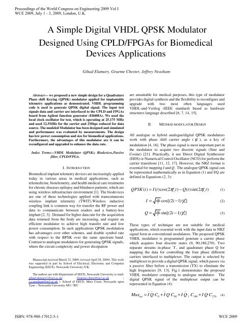
A Simple Digital VHDL QPSK Modulator Designed Using CPLD ...
A Simple Digital VHDL QPSK Modulator Designed Using CPLD ...
A Simple Digital VHDL QPSK Modulator Designed Using CPLD ...

You also want an ePaper? Increase the reach of your titles
YUMPU automatically turns print PDFs into web optimized ePapers that Google loves.
Proceedings of the World Congress on Engineering 2009 Vol I<br />
WCE 2009, July 1 - 3, 2009, London, U.K.<br />
A <strong>Simple</strong> <strong>Digital</strong> <strong>VHDL</strong> <strong>QPSK</strong> <strong>Modulator</strong><br />
<strong>Designed</strong> <strong>Using</strong> <strong>CPLD</strong>/FPGAs for Biomedical<br />
Devices Applications<br />
Abstract— we proposed a new simple design for a Quadrature<br />
Phase shift Keying (<strong>QPSK</strong>) modulator applied for implantable<br />
telemetry applications as demonstrated. <strong>VHDL</strong> programming<br />
code is used to generate <strong>QPSK</strong> digital signal. The input test<br />
signals data and carrier are interfaced to the <strong>CPLD</strong> and FPGAs<br />
board from Agilent function generator (E8408A). We used the<br />
local clock oscillator for test, which is operating at 25.175 MHz<br />
and used 12.5MHz for the carrier and 2Mbps reduced for data<br />
source. The modeled <strong>Modulator</strong> has been designed and simulated<br />
and performance was evaluated by measurements. The design<br />
has low power consumption and size for biomedical applications.<br />
Furthermore, the advantages of this modulator are it can be<br />
reconfigured and upgraded to enhance the data rate.<br />
Index Terms—<strong>VHDL</strong> <strong>Modulator</strong> (<strong>QPSK</strong>); Biodevices,Passive<br />
filter, <strong>CPLD</strong>/FPGA.<br />
I. INTRODUCTION<br />
Biomedical implant telemetry devices are increasingly applied<br />
today in various areas in medical applications, such as<br />
telemedicine, biotelemetry, and health medical care treatments<br />
for chronic diseases epilepsy and blindness patients; which are<br />
using wireless infrastructure environment [1]. The biodevices<br />
are one of these technologies applied with transcutaneous<br />
wireless implant telemetry (TWIT).Wireless inductive<br />
coupling link is common way for transfer the RF power and<br />
data to communicate between readers and a battery-less<br />
implant [2, 3]. Demand for higher data rate for the acquisition<br />
data returned from the body are increasing, and require an<br />
efficient modulator to achieve high transfer rate and low<br />
power consumption. In such applications <strong>QPSK</strong> modulation<br />
has advantages over other schemes, and double symbol rate<br />
with respect to the BPSK over the same spectrum band.<br />
Contrast to analogue modulators for generating <strong>QPSK</strong> signals,<br />
where the circuit complexity and power dissipation<br />
Manuscript received March 23, 2009; (revised April 28, 2009). This work<br />
was supported in part by School of Electrical, Electronic and Computer<br />
Engineering (EECE). Newcastle University /UK.<br />
The authors are with Department of EECE, Newcastle University (e-mail:<br />
gihad.elamary1@ncl.ac.uk; Graeme.chster@ncl.ac.uk ;<br />
j.a.neasham@ncl.ac.uk ). School of EECE- Merz Court, Newcastle upon<br />
Tyne – Newcastle University-NE1 7RU<br />
Gihad Elamary, Graeme Chester, Jeffrey Neasham<br />
are unsuitable for medical purposes, this type of modulator<br />
provides digital synthesis and the flexibility to reconfigure and<br />
upgrade with two most often languages used<br />
<strong>VHDL</strong>-and-Verilog (IEEE standard) based as hardware<br />
structures language described [6, 7, 14, 15].<br />
II. METHOD MODULATOR DESIGN<br />
All analogue or hybrid analogue/digital <strong>QPSK</strong> modulators<br />
work with phase shift carrier angle ( ϕ ), as a key of<br />
modulation [4, 16]. The phase signal is most important part in<br />
the modulator to acquire two discrete signals (Sine and<br />
Cosine) [21]. Practically, it use Direct <strong>Digital</strong> Synthesizer<br />
(DDS) or Numerical Control Oscillator (NCO) for perform the<br />
carrier transitions [11, 12, 17]. However, the NRZ format is<br />
essential for mapping I and Q. The analogue <strong>QPSK</strong> signal can<br />
be represented mathematically as in Equation (1) and I/Q are<br />
defined in Equations (2, 3):<br />
<strong>QPSK</strong> c<br />
c<br />
( t)<br />
= I(<br />
t)<br />
cos( 2πf<br />
t)<br />
− Q(<br />
t)<br />
sin( 2πf<br />
t)<br />
(1)<br />
2 I = 2i<br />
−1)<br />
π<br />
T ]<br />
E (2)<br />
Q T<br />
cos[( 4<br />
2E = sin[( 2i<br />
−1)<br />
π<br />
4]<br />
These types of technique are not suitable for medical<br />
applications, which essential work with the input data in NRZ<br />
signal form at conventional modulators. The proposed <strong>QPSK</strong><br />
<strong>VHDL</strong> modulator is programmed generate a carrier phase<br />
which acquires four discrete states (0, 90,180,270). Two<br />
separate streams in-phase ’I’, and quadrature phase Q for<br />
mapping the data for controlling the four phase different<br />
carriers interfaced to multiplexer. The output is selected by<br />
multiplexer to provide a digital <strong>QPSK</strong> signal, which passes via<br />
a passive filter before a transmission (TX) to eliminate the<br />
high frequencies [9, 13]. Fig.1 demonstrates the proposed<br />
<strong>VHDL</strong> modulator comparing to analogue modulator. The<br />
digital <strong>QPSK</strong> signal of the multiplexer output can be<br />
represented in Equation (4):<br />
− − −<br />
−<br />
Muxout = I Q⋅C0<br />
+ I Q⋅C90<br />
+ I Q⋅<br />
I<br />
C<br />
180<br />
+ I Q⋅C<br />
ISBN: 978-988-17012-5-1 WCE 2009<br />
270<br />
(3)<br />
(4)
Proceedings of the World Congress on Engineering 2009 Vol I<br />
WCE 2009, July 1 - 3, 2009, London, U.K.<br />
Figure 1. The block diagram for the proposed <strong>QPSK</strong> <strong>Modulator</strong><br />
III. FILTER DESIGN AND SIMULATION<br />
In wireless transmission we cannot transmit the digital signal<br />
directly without harmonics separation. The output of the<br />
multiplier is producing a <strong>QPSK</strong> digital signal “square signal”<br />
form. It is essential to use a filter to complete the process for<br />
the modulator “off-chip”. We designed an analogue passive<br />
filter for this purpose as it has zero power consumption. Two<br />
types of filters were investigated Low pass Filter (LPF) and<br />
Band Pass Filter (BPF) [5, 10,18], as appropriate for medical<br />
purpose the Butterworth LPF was given enhanced<br />
performance than other types of LP-filters, to eliminates the<br />
harmonics from the <strong>QPSK</strong> digital signal. While the second<br />
choice was the Chebyshev II Filter BPF this was observed to<br />
give better performance then other types of BP-filters. As<br />
demonstrated in Fig.2 and Equation (5).<br />
Mux<strong>Digital</strong> _ <strong>QPSK</strong><br />
S<strong>QPSK</strong> (LPF)<br />
S<strong>QPSK</strong> (BPF )<br />
Figure 2. The filters types used for harmonics eliminates<br />
S<strong>QPSK</strong><br />
( jw)<br />
H ( jw)<br />
= (5)<br />
Mux ( jw)<br />
out<br />
A. Butterworth LPF design and simulation<br />
Our prototype analogue filter selected is a Butterworth 4 th<br />
order to filter the input <strong>QPSK</strong> digital signal. The transfer<br />
function of LC filter can be represented in Equation (6). The<br />
simulation is presented in Fig. 3; with MATLAB/Simulink<br />
clearly it demonstrates the response of filter comparing to the<br />
Butterworth and Chebyshev I. Practically, a simple BW-LPF<br />
is designed to omit the harmonies and DC component. The<br />
size is implant where the filter is implanted with the modulator<br />
in biomedical devices.<br />
Figure 3. The LPF simulation with MATLAB/Simulink<br />
H ( s ) =<br />
S<br />
2<br />
LC<br />
2<br />
1<br />
+ SRC<br />
2<br />
+<br />
C<br />
2<br />
C<br />
1<br />
+ 1<br />
B. Chebyshev II HPF design and simulation<br />
The second prototype choice filter is Chebyshev II analogue<br />
passive LC filter 5 th order. The multiplexer output signal is fed<br />
into the designed filter. The simulation result with<br />
MATLAB/Simulink FFT is presented in Fig. 4. Which<br />
compares the Chebyshev I, Chebyshev II and Elliptic for<br />
performances type and characteristics. Obviously it gives a<br />
high separation, over 50dB.<br />
Figure 4. The BPF simulation with MATLAB/Simulink<br />
The simulation performances for other types of filters are<br />
presented in Table I as: (A) best performance (B) is less<br />
performance and (C) weak performance, and (NP) is Not<br />
Perfect performance.<br />
TABLE I. Influence of the investigation filters simulation<br />
Filter Types<br />
Butterworth Cheby I Cheby II Elliptic Bessel<br />
LPF A B NP C NP<br />
BPF NP NP A C B<br />
ISBN: 978-988-17012-5-1 WCE 2009<br />
(6)
Proceedings of the World Congress on Engineering 2009 Vol I<br />
WCE 2009, July 1 - 3, 2009, London, U.K.<br />
IV. LE SIMULATION<br />
A. MATLAB/Simulink simulation<br />
The <strong>QPSK</strong> modulator was designed and simulated with<br />
MATLAB/Simulink to verify and validate the modulator<br />
specifications [19]. The modulator is consists of carrier source<br />
to produce a periodic pulse signal ( f ), fed to a carrier<br />
carrier<br />
phase shifter; which shift the input carrier into four different<br />
phase signals (0°, 90°, 180°, 270°) interfaced to multiplexer.<br />
While the data source was generated with PN_suqance, fed to<br />
data mapping to generate I and Q signals to influence the four<br />
phase different carries. The output is selected by multiplexer<br />
which provides digital <strong>QPSK</strong> signal, this signal filtered with<br />
analogue filter before transmitted to pass fundamental<br />
frequency ( fo ± data ) and eliminates the higher frequencies<br />
associated with the square signal. The architecture block<br />
diagram of Tx_Mod is shown in Fig .6. The simulated random<br />
data signal (Data_in) which is generated by a PN sequence can<br />
be represented by Fourier series analysis as in Equation (6).<br />
PN( t)<br />
cn<br />
p(<br />
t − nTc<br />
)<br />
n=<br />
−∞<br />
(6)<br />
= ∑ ∞<br />
Where the input carrier signal is a periodic pulse train signal<br />
and mathematically expressed by the Fourier series as in<br />
Equation (7).<br />
4<br />
Carrier ( t ) =<br />
π<br />
∑ ∞<br />
n = 1<br />
sin(( 2 n − 1)<br />
w ct<br />
)<br />
( 2 n − 1)<br />
The Tx and the Rx signals are presented in Fig. 5 shows the<br />
spectrum of the transmitted RF signal (CH1) and the received<br />
RF signal (CH2) in the presence of noise (AWGN).<br />
Figure 6. The propoused <strong>Modulator</strong> with Mathlab /simulink daigram<br />
Figure 5. The specrum of <strong>QPSK</strong> transmit and rceive signals<br />
at Data rate 2Mbps,carrier 12.5MHz<br />
ISBN: 978-988-17012-5-1 WCE 2009<br />
(7)
Proceedings of the World Congress on Engineering 2009 Vol I<br />
WCE 2009, July 1 - 3, 2009, London, U.K.<br />
B. <strong>VHDL</strong> programming code simulation<br />
The proposed modulator was built by the Altera UP2<br />
development kit board [8], Programmed with the <strong>VHDL</strong><br />
language for modeling, design and analysis of the proposed<br />
<strong>QPSK</strong> modulator. The simulated result of this modulator is<br />
presented in Fig.7. This demonstrates the output signals<br />
waveforms indicating the transitions (180°, 270°) of the<br />
carrier signal influence by input data signal. The carrier<br />
frequency 12.5 MHz was generated from the local clock<br />
signal on the board, which operates at 25.175 MHz. The data<br />
signal was reduced to 2 MHz by a frequency divider then fed<br />
into a random PN_sequence generator (behavioral<br />
described).The modulator was implemented and comparing<br />
two different designs structural and behavior descriptions; for<br />
efficient performance. The generated <strong>VHDL</strong> “Behavioral”<br />
block diagram of the <strong>QPSK</strong> modulator is illustrated in Fig. 8<br />
Figure 8. The porporsed <strong>VHDL</strong> modulator<br />
Figure 7. The propoused <strong>Modulator</strong> with Mathlab /simulink daigra<br />
V. Experimental results and discussion<br />
In this part of paper, we provide the measurements which<br />
were conducted using the Altera UP2 Development kit board,<br />
for testing the <strong>VHDL</strong> code modulator and comparing the<br />
performance with the simulated <strong>QPSK</strong> modulation. The<br />
Agilent digital demodulator (E8408A VXI) is used to receive<br />
the filtered RF <strong>QPSK</strong> signal, and analyzed the parameters of<br />
the transmitted <strong>QPSK</strong> signal (Tx) as demonstrated in Fig. 9<br />
[22]. The desired carrier signal was generated from the master<br />
clock on the circuit board that operates at 25.175 MHz, using<br />
12.5 MHz as carrier. The carrier phase acquires four discrete<br />
states (0, π 2 , π , 3π<br />
2 ). This corresponds to mapping I<br />
and Q data source generated with <strong>VHDL</strong> code inside the<br />
<strong>CPLD</strong>/FPGAs at 2Mbps. The signal passes as digital <strong>QPSK</strong><br />
through the passive LPF for harmonics separation.<br />
Figure 9. Illustrated the setup Lab measurement withUK2 Alter<br />
ISBN: 978-988-17012-5-1 WCE 2009
Proceedings of the World Congress on Engineering 2009 Vol I<br />
WCE 2009, July 1 - 3, 2009, London, U.K.<br />
We investigated two prototypes of filters in this paper, LPF<br />
and BPF. The BPF has a better performance characteristic<br />
then LPF. However, the measurement result was illustrated in<br />
Fig. 10 as; (a) PN_code signal generated by <strong>VHDL</strong> code, (b)<br />
the <strong>QPSK</strong> digital signal, (c) the filtered signal output. While<br />
the spectrum of Tx signal was captured with signal analyzer in<br />
Agilent (8408A) at center frequency 12.58MHz as<br />
demonstrated in Fig 11. The demodulator is also constructed<br />
using the Matlab/Simulink tools to examine the performance<br />
of the proposed modulator. The performance has measured<br />
using Agilent Education version to demodulate the received<br />
signal “<strong>QPSK</strong> Demodulator” to demodulate the information<br />
data, which was transmitted with <strong>VHDL</strong> modulator. The<br />
measurement results are given respectively in Fig .12, the<br />
constellation diagram for <strong>QPSK</strong> Rx signal, and Fig.13<br />
illustrating the spectrum and the demodulated data at 2Mbps.<br />
Ultimately, the whole bench test system is illustrated in Fig<br />
.14<br />
Figure 10. Measured <strong>QPSK</strong> digital siganl (a); PN-code<br />
;(b)<strong>Digital</strong> signal (c ) filter signal throgh LPF<br />
Figure 11. The Tx Spectrum of the <strong>QPSK</strong> transmitted signal at<br />
carrier 12.5MH<br />
Figure 12. Constellation diagram of <strong>QPSK</strong> demoulator received<br />
from proposed <strong>QPSK</strong> modulator<br />
Figure 13. Spectrum of the <strong>QPSK</strong> deomulator recivced signal<br />
from proposed <strong>QPSK</strong> mod at carrier (12.58Mhz), data (2Mbps)<br />
Figure 14. Illustrates the test bench Lab measurement for transmit<br />
data over wireless inductive link using Agilent demodulator<br />
ISBN: 978-988-17012-5-1 WCE 2009
Proceedings of the World Congress on Engineering 2009 Vol I<br />
WCE 2009, July 1 - 3, 2009, London, U.K.<br />
VI. CONCLUSION<br />
We implemented a new simple direct <strong>QPSK</strong> digital modulator<br />
model in MATLAB/Simulink environment. It has been<br />
successfully designed with <strong>VHDL</strong> programming code by<br />
Altera development kit. The modulator generate <strong>QPSK</strong><br />
signal directly from binary digital data. For test purpose it was<br />
generated with <strong>VHDL</strong> code inside the <strong>CPLD</strong>/FPGA, mapped<br />
for I / Q to control the carrier signal using <strong>VHDL</strong> multiplexer<br />
code. The output producing modulated digital signal, filtered<br />
to transmit through designed filters (LPF/BPF).<br />
Experimentally measurements were presented at carrier<br />
frequency 12.50 MHz; and data rate 2Mbps. Which presents<br />
better performance with high data rate and carrier suppression<br />
about ~ 40dB. The filter is main key in the design, eventually<br />
we designed and simulated for optimum passive filter for<br />
implant part, and comparing to the better filter performances.<br />
However, the simulation results given the better performance<br />
if we selected the BPF Chebyshev I & II types, comparing to<br />
others. On other hand the Butterworth LPF type gave<br />
optimum performance. The disadvantage of digital filter is it<br />
needs higher sampling frequencies which increase the<br />
consumption power and size. These are not considering in this<br />
work. Furthermore, additional work was done to test the<br />
proposed modulator over wireless inductive coupling, which<br />
gave better received data wirelessly up to 3Mbps over<br />
distance about 9.5cm. Eventually this technique can offer<br />
high transfer rate for biomedical devices requiring a high<br />
demand rate, such as electrodes information measured in real<br />
time, where the acquisitions data from electrodes are<br />
increasing form the neural system. Ultimately, in future work,<br />
it is also an intention to up-convert the signal into an ISM<br />
unlicensed frequency in UHF band (402~ 405 MHz). For<br />
biomedical telemetry applications, increasing the data rate<br />
with low noise and size reduced.<br />
REFERENCES<br />
[1] K.Wise, D.Anderson, J.Hetke, R.Kipke, K.Najafi “Wireless<br />
implantable Microsystems High density Electronics interfaces to the<br />
nervous system”IEEE , Proceeding ,Vol.92,pp. 76-97, 2004.<br />
[2] Ghazi Ben Hmida, Mhommed Dhieb, Hamadi Gharinai, Mounir Samet<br />
“ Transcutaneous Power and High Data Rata Transmission For<br />
Biomedical Implants ” 2006 IEEE.<br />
[3] S.Atluri, M.Ghovanloo “<strong>Digital</strong> of wideband power efficiency<br />
inductive wireless link for implantable biomedical using multiple<br />
carriers” Internal conference EMBS on neural engineering. IEEE, 2005<br />
[4] A. M. El-Gabaly, B. R. Jackson and C. E. Saavedra, "An L-Band<br />
Direct-<strong>Digital</strong> <strong>QPSK</strong> <strong>Modulator</strong> in CMOS," IEEE International<br />
Symposium on Signals, Systems and Electronics, Montreal, Quebec,<br />
Canada, April 2007.<br />
[5] B.Williams and Fred.J.Taylor, “Electronic Filter Design Handbook,”<br />
by the McGarw-Hill companies, vol. III, G. T. Rado and H. Suhl, Eds.<br />
USA: 2006, pp. 89–137,pp.165-239.<br />
[6] G.C.Cardarilli, R. A.Del Re.RE, L.Simone Nicol, “Otimized <strong>QPSK</strong><br />
Modulaator for DVB-S Applications,” ISCAS 2006 IEEE .<br />
[7] Douglas.L.Perry “<strong>VHDL</strong> Programming by Example”Mc.Grawh. USA:<br />
Academic 2002, pp. 842- 868<br />
[8] www.altera.com/literature/univ/upds.pdf.(UP2 edicational board<br />
datasheet).<br />
[9] Roger.Lipsett,Carl.Schaefer, Cary.Ussery “<strong>VHDL</strong> Hardware<br />
Description and design” pp842-868<br />
[10] H.Bochnick,W.Anheier “FIR filter design using Verilog and<br />
<strong>VHDL</strong>”.Italy April.16-26.1993<br />
[11] He.Jin,He.Song.Ben “Design and Realization on NCO of modulator<br />
based on FPGA ”IEEE, communiocation Circuit and system ICCCAS<br />
11-13.july .2007, pp 831-833.<br />
[12] J.Goncalves, J.R.Fernandes,M.MSilva “A Reconfigurable Quadrature<br />
Oscillator Based on a Dirct <strong>Digital</strong> Synthesis System” DCIS, 2006<br />
[13] M.Kovac,J.kolouch “BPSK,<strong>QPSK</strong> MODULATOR SIMULATION<br />
MODUEL”2004<br />
[14] E.Normark,Lei.Yang,C.Wakayama,P.Nikitin,R,Shi “<strong>VHDL</strong> –AMS<br />
Beahvioral Modeling and simulation of api/4D<strong>QPSK</strong> transceiver<br />
system”<br />
[15] http://ieeexplore.ieee.org/iel5/7180/19335/00893288.pdf( “ IEEE<br />
standred <strong>VHDL</strong> Language Reference Manual ”<br />
[16] http://www.complextoreal.com/chapters/mod1.pdf, (Intuititive giude<br />
to the principles commuincation )<br />
[17] I.Janiszwski, B.H.Meuth “Numerically controlled oscillators with<br />
Hybrid function generators ”IEEE transction on<br />
ultrasonics,Vol,49,No.7,July2002<br />
[18] T.J.Kazmierski,F.A.Hamid “Architectural and parametric<br />
optimization of low-pass RF anloge Filter in <strong>VHDL</strong> – AMS based high<br />
level synthsis ”BMAS2004,San Jose,20-22 oct2004-2.<br />
[19] http://www.mathworks.co.uk/support/. ( Matlab / Simulink sources )<br />
[20] www.analog.com/.../archives/38-08/dds.html ( Data sheet of Direct<br />
<strong>Digital</strong> Synthesiser form analog devices)<br />
[21] http://www.home.agilent.com/agilent/product. ( <strong>Digital</strong> modulator /<br />
demodualtor Agilent E8408A VXI)<br />
ISBN: 978-988-17012-5-1 WCE 2009