A Simple Digital VHDL QPSK Modulator Designed Using CPLD ...
A Simple Digital VHDL QPSK Modulator Designed Using CPLD ...
A Simple Digital VHDL QPSK Modulator Designed Using CPLD ...

You also want an ePaper? Increase the reach of your titles
YUMPU automatically turns print PDFs into web optimized ePapers that Google loves.
Proceedings of the World Congress on Engineering 2009 Vol I<br />
WCE 2009, July 1 - 3, 2009, London, U.K.<br />
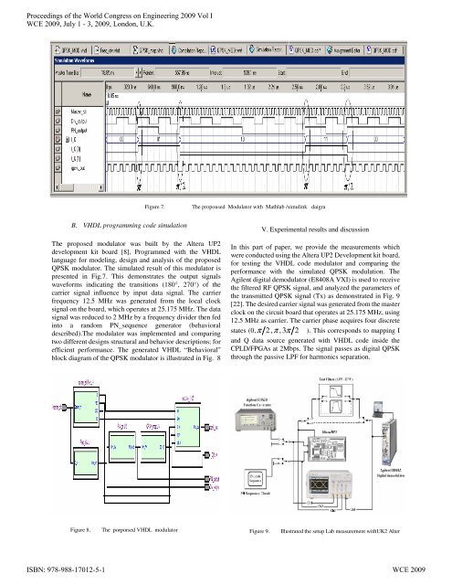
B. <strong>VHDL</strong> programming code simulation<br />
The proposed modulator was built by the Altera UP2<br />
development kit board [8], Programmed with the <strong>VHDL</strong><br />
language for modeling, design and analysis of the proposed<br />
<strong>QPSK</strong> modulator. The simulated result of this modulator is<br />
presented in Fig.7. This demonstrates the output signals<br />
waveforms indicating the transitions (180°, 270°) of the<br />
carrier signal influence by input data signal. The carrier<br />
frequency 12.5 MHz was generated from the local clock<br />
signal on the board, which operates at 25.175 MHz. The data<br />
signal was reduced to 2 MHz by a frequency divider then fed<br />
into a random PN_sequence generator (behavioral<br />
described).The modulator was implemented and comparing<br />
two different designs structural and behavior descriptions; for<br />
efficient performance. The generated <strong>VHDL</strong> “Behavioral”<br />
block diagram of the <strong>QPSK</strong> modulator is illustrated in Fig. 8<br />
Figure 8. The porporsed <strong>VHDL</strong> modulator<br />
Figure 7. The propoused <strong>Modulator</strong> with Mathlab /simulink daigra<br />
V. Experimental results and discussion<br />
In this part of paper, we provide the measurements which<br />
were conducted using the Altera UP2 Development kit board,<br />
for testing the <strong>VHDL</strong> code modulator and comparing the<br />
performance with the simulated <strong>QPSK</strong> modulation. The<br />
Agilent digital demodulator (E8408A VXI) is used to receive<br />
the filtered RF <strong>QPSK</strong> signal, and analyzed the parameters of<br />
the transmitted <strong>QPSK</strong> signal (Tx) as demonstrated in Fig. 9<br />
[22]. The desired carrier signal was generated from the master<br />
clock on the circuit board that operates at 25.175 MHz, using<br />
12.5 MHz as carrier. The carrier phase acquires four discrete<br />
states (0, π 2 , π , 3π<br />
2 ). This corresponds to mapping I<br />
and Q data source generated with <strong>VHDL</strong> code inside the<br />
<strong>CPLD</strong>/FPGAs at 2Mbps. The signal passes as digital <strong>QPSK</strong><br />
through the passive LPF for harmonics separation.<br />
Figure 9. Illustrated the setup Lab measurement withUK2 Alter<br />
ISBN: 978-988-17012-5-1 WCE 2009