Low Cost DC-500 MHz 92 dB Logarithmic Amplifier AD8307 CMOScompatible
AD8307 Low Cost DC-500 MHz, 92 dB Logarithmic ... - Ok1dfc.com
AD8307 Low Cost DC-500 MHz, 92 dB Logarithmic ... - Ok1dfc.com
- No tags were found...

You also want an ePaper? Increase the reach of your titles
YUMPU automatically turns print PDFs into web optimized ePapers that Google loves.
<strong>AD8307</strong><br />
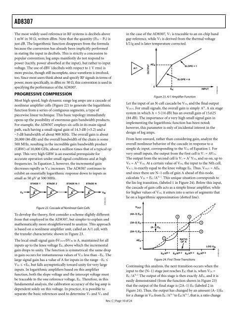
The most widely used reference in RF systems is decibels above<br />
1 mW in 50 Ω, written <strong>dB</strong>m. Note that the quantity (PIN – P0) is<br />
just <strong>dB</strong>. The logarithmic function disappears from the formula<br />
because the conversion has already been implicitly performed<br />
in stating the input in decibels. This is strictly a concession to<br />
popular convention; log amps manifestly do not respond to<br />
power (tacitly, power absorbed at the input), but rather to input<br />
voltage. The use of <strong>dB</strong>V (decibels with respect to 1 V rms) is<br />
more precise, though still incomplete, since waveform is involved,<br />
too. Since most users think about and specify RF signals in terms of<br />
power, more specifically, in <strong>dB</strong>m re: 50 Ω, this convention is used in<br />
specifying the performance of the <strong>AD8307</strong>.<br />
PROGRESSIVE COMPRESSION<br />
Most high speed, high dynamic range log amps use a cascade of<br />
nonlinear amplifier cells (Figure 22) to generate the logarithmic<br />
function from a series of contiguous segments, a type of<br />
piecewise linear technique. This basic topology immediately<br />
opens up the possibility of enormous gain bandwidth products.<br />
For example, the <strong>AD8307</strong> employs six cells in its main signal<br />
path, each having a small signal gain of 14.3 <strong>dB</strong> (×5.2) and a<br />
−3 <strong>dB</strong> bandwidth of about 900 <strong>MHz</strong>. The overall gain is about<br />
20,000 (86 <strong>dB</strong>) and the overall bandwidth of the chain is some<br />
<strong>500</strong> <strong>MHz</strong>, resulting in the incredible gain bandwidth product<br />
(GBW) of 10,000 GHz, about a million times that of a typical op<br />
amp. This very high GBW is an essential prerequisite for<br />
accurate operation under small signal conditions and at high<br />
frequencies. In Equation 2, however, the incremental gain<br />
decreases rapidly as VIN increases. The <strong>AD8307</strong> continues to<br />
exhibit an essentially logarithmic response down to inputs as<br />
small as 50 μV at <strong>500</strong> <strong>MHz</strong>.<br />
V X<br />
STAGE 1 STAGE 2 STAGE N–1 STAGE N<br />
A A A A<br />
Figure 22. Cascade of Nonlinear Gain Cells<br />
To develop the theory, first consider a scheme slightly different<br />
from that employed in the <strong>AD8307</strong>, but simpler to explain and<br />
mathematically more straightforward to analyze. This approach<br />
is based on a nonlinear amplifier unit, called an A/1 cell, with<br />
the transfer characteristic shown in Figure 23.<br />
The local small signal gain δVOUT/δVIN is A, maintained for all<br />
inputs up to the knee voltage EK, above which the incremental<br />
gain drops to unity. The function is symmetrical: the same drop<br />
in gain occurs for instantaneous values of VIN less than –EK. The<br />
large signal gain has a value of A for inputs in the range −EK ≤<br />
VIN ≤ +EK, but falls asymptotically toward unity for very large<br />
inputs. In logarithmic amplifiers based on this amplifier<br />
function, both the slope voltage and the intercept voltage must<br />
be traceable to the one reference voltage, EK. Therefore, in this<br />
fundamental analysis, the calibration accuracy of the log amp is<br />
dependent solely on this voltage. In practice, it is possible to<br />
separate the basic references used to determine VY and VX and<br />
V W<br />
01082-022<br />
Rev. C | Page 10 of 24<br />
in the case of the <strong>AD8307</strong>, VY is traceable to an on-chip band<br />
gap reference, while VX is derived from the thermal voltage<br />
kT/q and is later temperature corrected.<br />
A/1<br />
OUTPUT<br />
AE K<br />
0<br />
E K<br />
SLOPE = A<br />
SLOPE = 1<br />
Figure 23. A/1 <strong>Amplifier</strong> Function<br />
INPUT<br />
Let the input of an N-cell cascade be VIN, and the final output<br />
VOUT. For small signals, the overall gain is simply A N . A six stage<br />
system in which A = 5 (14 <strong>dB</strong>) has an overall gain of 15,625<br />
(84 <strong>dB</strong>). The importance of a very high small signal gain in<br />
implementing the logarithmic function has been noted;<br />
however, this parameter is only of incidental interest in the<br />
design of log amps.<br />
From here onward, rather than considering gain, analyze the<br />
overall nonlinear behavior of the cascade in response to a<br />
simple dc input, corresponding to the VIN of Equation 1. For<br />
very small inputs, the output from the first cell is V1 = AVIN.<br />
The output from the second cell is V2 = A 2 VIN, and so on, up to<br />
VN = A N VIN. At a certain value of VIN, the input to the Nth cell,<br />
VN–1, is exactly equal to the knee voltage EK. Thus, VOUT = AEK<br />
and since there are N–1 cells of gain A ahead of this node,<br />
calculate VIN = EK /A N–1 . This unique situation corresponds to<br />
the lin-log transition, (labeled 1 in Figure 24). Below this input,<br />
the cascade of gain cells acts as a simple linear amplifier, while<br />
for higher values of VIN, it enters into a series of segments that<br />
lie on a logarithmic approximation (dotted line).<br />
V OUT<br />
(4A–3) E K<br />
(3A–2) E K<br />
(2A–1) E K<br />
AE K<br />
0<br />
(A–1) E K<br />
1<br />
2<br />
RATIO<br />
OF A<br />
E K /A N–1 E K /A N–2 E K /A N–3 E K /A N–4 LOG V IN<br />
Figure 24. First Three Transitions<br />
Continuing this analysis, the next transition occurs when the<br />
input to the (N–1) stage just reaches EK; that is, when VIN =<br />
EK /A N–2 . The output of this stage is then exactly AEK, and it is<br />
easily demonstrated (from the function shown in Figure 23)<br />
that the output of the final stage is (2A–1) EK (labeled 2 in<br />
Figure 24). Thus, the output has changed by an amount (A–1)EK<br />
for a change in VIN from EK /A N–1 to EK/A N–2 , that is, a ratio change<br />
3<br />
3<br />
2<br />
01082-023<br />
01082-024