Low Cost DC-500 MHz 92 dB Logarithmic Amplifier AD8307 CMOScompatible
AD8307 Low Cost DC-500 MHz, 92 dB Logarithmic ... - Ok1dfc.com
AD8307 Low Cost DC-500 MHz, 92 dB Logarithmic ... - Ok1dfc.com
- No tags were found...

Create successful ePaper yourself
Turn your PDF publications into a flip-book with our unique Google optimized e-Paper software.
<strong>AD8307</strong><br />
frequency range, a turns ratio of about 1:4.8 lowers the input<br />
impedance to 50 Ω while raising the input voltage, thus<br />
lowering the effect of the short-circuit noise voltage by the same<br />
factor. There is a small contribution from the input noise<br />
current, so the total noise is reduced by a lesser factor. The<br />
intercept is also lowered by the turns ratio; for a 50 Ω match, it<br />
is reduced by 20 log10 (4.8) or 13.6 <strong>dB</strong>.<br />
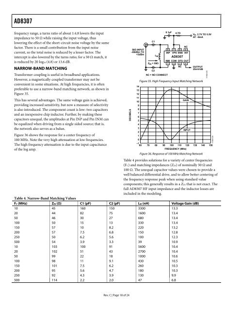
NARROW-BAND MATCHING<br />
Transformer coupling is useful in broadband applications.<br />
However, a magnetically-coupled transformer may not be<br />
convenient in some situations. At high frequencies, it is often<br />
preferable to use a narrow-band matching network, as shown in<br />
Figure 35.<br />
This has several advantages. The same voltage gain is achieved,<br />
providing increased sensitivity, but now a measure of selectivity<br />
is also introduced. The component count is low: two capacitors<br />
and an inexpensive chip inductor. Further, by making these<br />
capacitors unequal, the amplitudes at Pin INP and Pin INM can<br />
be equalized when driving from a single sided source; that is,<br />
the network also serves as a balun.<br />
Figure 36 shows the response for a center frequency of<br />
100 <strong>MHz</strong>. Note the very high attenuation at low frequencies.<br />
The high frequency attenuation is due to the input capacitance<br />
of the log amp.<br />
DECIBELS<br />
50Ω INPUT<br />
–88<strong>dB</strong>m TO<br />
+3<strong>dB</strong>m<br />
14<br />
13<br />
12<br />
11<br />
10<br />
9<br />
8<br />
7<br />
6<br />
5<br />
4<br />
3<br />
2<br />
1<br />
0<br />
V , 2.7V TO 5.5V<br />
0.1µF 4.7Ω<br />
L M<br />
P<br />
AT ~8mA<br />
C1<br />
NC<br />
8 7 6 5<br />
INP VPS ENB INT<br />
Z IN = 50Ω<br />
C2<br />
NC = NO CONNECT<br />
<strong>AD8307</strong><br />
INM COM OFS OUT<br />
1 2 3 4<br />
NC<br />
OUTPUT<br />
25mV/<strong>dB</strong><br />
Figure 35. High Frequency Input Matching Network<br />
GAIN<br />
INPUT<br />
–1<br />
60 70 80 90 100 110 120 130 140 150<br />
FREQUENCY (<strong>MHz</strong>)<br />
Figure 36. Response of 100 <strong>MHz</strong> Matching Network<br />
Table 4 provides solutions for a variety of center frequencies<br />
(FC) and matching impedances (ZIN) of nominally 50 Ω and<br />
100 Ω. The unequal capacitor values were chosen to provide a<br />
well balanced differential drive, and to allow better centering of<br />
the frequency response peak when using standard value<br />
components; this generally results in a ZIN that is not exact. The<br />
full <strong>AD8307</strong> HF input impedance and the inductor losses are<br />
included in the modeling.<br />
Table 4. Narrow-Band Matching Values<br />
FC (<strong>MHz</strong>) ZIN (Ω) C1 (pF) C2 (pF) LM (nH) Voltage Gain (<strong>dB</strong>)<br />
10 45 160 150 3300 13.3<br />
20 44 82 75 1600 13.4<br />
50 46 30 27 680 13.4<br />
100 50 15 13 330 13.4<br />
150 57 10 8.2 220 13.2<br />
200 57 7.5 6.8 150 12.8<br />
250 50 6.2 5.6 100 12.3<br />
<strong>500</strong> 54 3.9 3.3 39 10.9<br />
10 103 100 91 5600 10.4<br />
20 102 51 43 2700 10.4<br />
50 99 22 18 1000 10.6<br />
100 98 11 9.1 430 10.5<br />
150 101 7.5 6.2 260 10.3<br />
200 95 5.6 4.7 180 10.3<br />
250 <strong>92</strong> 4.3 3.9 130 9.9<br />
<strong>500</strong> 114 2.2 2.0 47 6.8<br />
01082-035<br />
01082-036<br />
Rev. C | Page 18 of 24