Low Cost DC-500 MHz 92 dB Logarithmic Amplifier AD8307 CMOScompatible
AD8307 Low Cost DC-500 MHz, 92 dB Logarithmic ... - Ok1dfc.com
AD8307 Low Cost DC-500 MHz, 92 dB Logarithmic ... - Ok1dfc.com
- No tags were found...

Create successful ePaper yourself
Turn your PDF publications into a flip-book with our unique Google optimized e-Paper software.
<strong>AD8307</strong><br />
V IN<br />
A/0 A/0<br />
g m<br />
AV IN A 2 V IN A 3 V IN A 4 V IN<br />
g m<br />
A/0<br />
g m<br />
A/0<br />
g m<br />
g m<br />
V LIM<br />
I OUT<br />
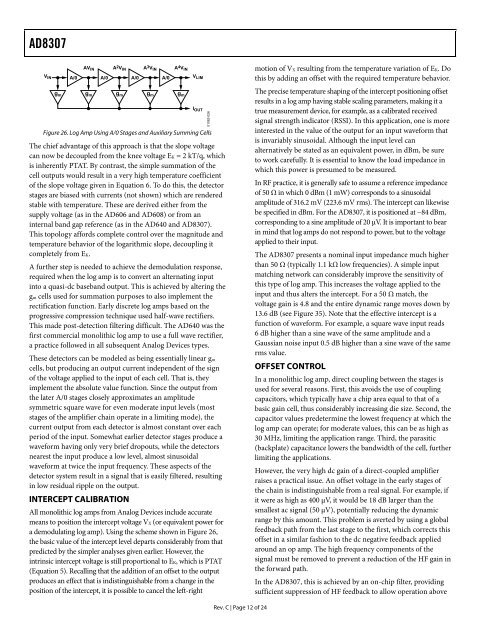
Figure 26. Log Amp Using A/0 Stages and Auxiliary Summing Cells<br />
The chief advantage of this approach is that the slope voltage<br />
can now be decoupled from the knee voltage EK = 2 kT/q, which<br />
is inherently PTAT. By contrast, the simple summation of the<br />
cell outputs would result in a very high temperature coefficient<br />
of the slope voltage given in Equation 6. To do this, the detector<br />
stages are biased with currents (not shown) which are rendered<br />
stable with temperature. These are derived either from the<br />
supply voltage (as in the AD606 and AD608) or from an<br />
internal band gap reference (as in the AD640 and <strong>AD8307</strong>).<br />
This topology affords complete control over the magnitude and<br />
temperature behavior of the logarithmic slope, decoupling it<br />
completely from EK.<br />
A further step is needed to achieve the demodulation response,<br />
required when the log amp is to convert an alternating input<br />
into a quasi-dc baseband output. This is achieved by altering the<br />
gm cells used for summation purposes to also implement the<br />
rectification function. Early discrete log amps based on the<br />
progressive compression technique used half-wave rectifiers.<br />
This made post-detection filtering difficult. The AD640 was the<br />
first commercial monolithic log amp to use a full wave rectifier,<br />
a practice followed in all subsequent Analog Devices types.<br />
These detectors can be modeled as being essentially linear gm<br />
cells, but producing an output current independent of the sign<br />
of the voltage applied to the input of each cell. That is, they<br />
implement the absolute value function. Since the output from<br />
the later A/0 stages closely approximates an amplitude<br />
symmetric square wave for even moderate input levels (most<br />
stages of the amplifier chain operate in a limiting mode), the<br />
current output from each detector is almost constant over each<br />
period of the input. Somewhat earlier detector stages produce a<br />
waveform having only very brief dropouts, while the detectors<br />
nearest the input produce a low level, almost sinusoidal<br />
waveform at twice the input frequency. These aspects of the<br />
detector system result in a signal that is easily filtered, resulting<br />
in low residual ripple on the output.<br />
INTERCEPT CALIBRATION<br />
All monolithic log amps from Analog Devices include accurate<br />
means to position the intercept voltage VX (or equivalent power for<br />
a demodulating log amp). Using the scheme shown in Figure 26,<br />
the basic value of the intercept level departs considerably from that<br />
predicted by the simpler analyses given earlier. However, the<br />
intrinsic intercept voltage is still proportional to EK, which is PTAT<br />
(Equation 5). Recalling that the addition of an offset to the output<br />
produces an effect that is indistinguishable from a change in the<br />
position of the intercept, it is possible to cancel the left-right<br />
01082-026<br />
motion of VX resulting from the temperature variation of EK. Do<br />
this by adding an offset with the required temperature behavior.<br />
The precise temperature shaping of the intercept positioning offset<br />
results in a log amp having stable scaling parameters, making it a<br />
true measurement device, for example, as a calibrated received<br />
signal strength indicator (RSSI). In this application, one is more<br />
interested in the value of the output for an input waveform that<br />
is invariably sinusoidal. Although the input level can<br />
alternatively be stated as an equivalent power, in <strong>dB</strong>m, be sure<br />
to work carefully. It is essential to know the load impedance in<br />
which this power is presumed to be measured.<br />
In RF practice, it is generally safe to assume a reference impedance<br />
of 50 Ω in which 0 <strong>dB</strong>m (1 mW) corresponds to a sinusoidal<br />
amplitude of 316.2 mV (223.6 mV rms). The intercept can likewise<br />
be specified in <strong>dB</strong>m. For the <strong>AD8307</strong>, it is positioned at −84 <strong>dB</strong>m,<br />
corresponding to a sine amplitude of 20 μV. It is important to bear<br />
in mind that log amps do not respond to power, but to the voltage<br />
applied to their input.<br />
The <strong>AD8307</strong> presents a nominal input impedance much higher<br />
than 50 Ω (typically 1.1 kΩ low frequencies). A simple input<br />
matching network can considerably improve the sensitivity of<br />
this type of log amp. This increases the voltage applied to the<br />
input and thus alters the intercept. For a 50 Ω match, the<br />
voltage gain is 4.8 and the entire dynamic range moves down by<br />
13.6 <strong>dB</strong> (see Figure 35). Note that the effective intercept is a<br />
function of waveform. For example, a square wave input reads<br />
6 <strong>dB</strong> higher than a sine wave of the same amplitude and a<br />
Gaussian noise input 0.5 <strong>dB</strong> higher than a sine wave of the same<br />
rms value.<br />
OFFSET CONTROL<br />
In a monolithic log amp, direct coupling between the stages is<br />
used for several reasons. First, this avoids the use of coupling<br />
capacitors, which typically have a chip area equal to that of a<br />
basic gain cell, thus considerably increasing die size. Second, the<br />
capacitor values predetermine the lowest frequency at which the<br />
log amp can operate; for moderate values, this can be as high as<br />
30 <strong>MHz</strong>, limiting the application range. Third, the parasitic<br />
(backplate) capacitance lowers the bandwidth of the cell, further<br />
limiting the applications.<br />
However, the very high dc gain of a direct-coupled amplifier<br />
raises a practical issue. An offset voltage in the early stages of<br />
the chain is indistinguishable from a real signal. For example, if<br />
it were as high as 400 μV, it would be 18 <strong>dB</strong> larger than the<br />
smallest ac signal (50 μV), potentially reducing the dynamic<br />
range by this amount. This problem is averted by using a global<br />
feedback path from the last stage to the first, which corrects this<br />
offset in a similar fashion to the dc negative feedback applied<br />
around an op amp. The high frequency components of the<br />
signal must be removed to prevent a reduction of the HF gain in<br />
the forward path.<br />
In the <strong>AD8307</strong>, this is achieved by an on-chip filter, providing<br />
sufficient suppression of HF feedback to allow operation above<br />
Rev. C | Page 12 of 24