Low Cost DC-500 MHz 92 dB Logarithmic Amplifier AD8307 CMOScompatible
AD8307 Low Cost DC-500 MHz, 92 dB Logarithmic ... - Ok1dfc.com
AD8307 Low Cost DC-500 MHz, 92 dB Logarithmic ... - Ok1dfc.com
- No tags were found...

Create successful ePaper yourself
Turn your PDF publications into a flip-book with our unique Google optimized e-Paper software.
<strong>AD8307</strong><br />
2.50<br />
2.25<br />
2.00<br />
1.75<br />
WITHOUT<br />
FILTER<br />
2<br />
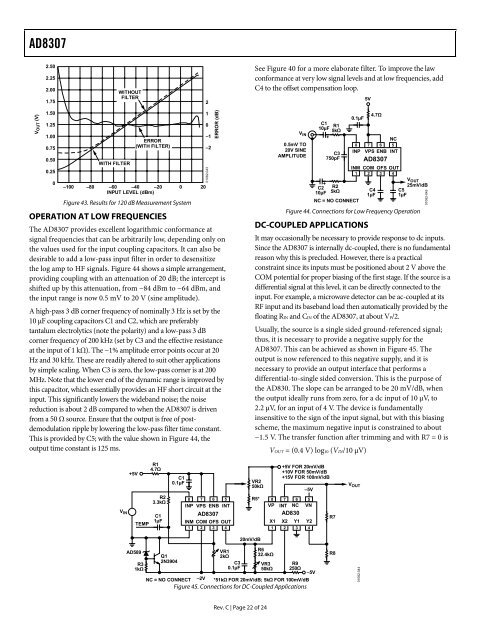
See Figure 40 for a more elaborate filter. To improve the law<br />
conformance at very low signal levels and at low frequencies, add<br />
C4 to the offset compensation loop.<br />
5V<br />
V OUT (V)<br />
1.50<br />
1.25<br />
1.00<br />
0.75<br />
0.50<br />
0.25<br />
0<br />
WITH FILTER<br />
ERROR<br />
(WITH FILTER)<br />
–100 –80 –60 –40 –20 0 20<br />
INPUT LEVEL (<strong>dB</strong>m)<br />
Figure 43. Results for 120 <strong>dB</strong> Measurement System<br />
OPERATION AT LOW FREQUENCIES<br />
The <strong>AD8307</strong> provides excellent logarithmic conformance at<br />
signal frequencies that can be arbitrarily low, depending only on<br />
the values used for the input coupling capacitors. It can also be<br />
desirable to add a low-pass input filter in order to desensitize<br />
the log amp to HF signals. Figure 44 shows a simple arrangement,<br />
providing coupling with an attenuation of 20 <strong>dB</strong>; the intercept is<br />
shifted up by this attenuation, from −84 <strong>dB</strong>m to −64 <strong>dB</strong>m, and<br />
the input range is now 0.5 mV to 20 V (sine amplitude).<br />
A high-pass 3 <strong>dB</strong> corner frequency of nominally 3 Hz is set by the<br />
10 μF coupling capacitors C1 and C2, which are preferably<br />
tantalum electrolytics (note the polarity) and a low-pass 3 <strong>dB</strong><br />
corner frequency of 200 kHz (set by C3 and the effective resistance<br />
at the input of 1 kΩ). The −1% amplitude error points occur at 20<br />
Hz and 30 kHz. These are readily altered to suit other applications<br />
by simple scaling. When C3 is zero, the low-pass corner is at 200<br />
<strong>MHz</strong>. Note that the lower end of the dynamic range is improved by<br />
this capacitor, which essentially provides an HF short circuit at the<br />
input. This significantly lowers the wideband noise; the noise<br />
reduction is about 2 <strong>dB</strong> compared to when the <strong>AD8307</strong> is driven<br />
from a 50 Ω source. Ensure that the output is free of postdemodulation<br />
ripple by lowering the low-pass filter time constant.<br />
This is provided by C5; with the value shown in Figure 44, the<br />
output time constant is 125 ms.<br />
1<br />
0<br />
–1<br />
–2<br />
01082-043<br />
ERROR (<strong>dB</strong>)<br />
V IN<br />
0.5mV TO<br />
20V SINE<br />
AMPLITUDE<br />
C1<br />
R1<br />
10µF<br />
5kΩ<br />
+<br />
C3<br />
750pF<br />
0.1µF<br />
+<br />
C2 R2<br />
10µF 5kΩ<br />
NC = NO CONNECT<br />
4.7Ω<br />
NC<br />
8 7 6 5<br />
INP VPS ENB INT<br />
<strong>AD8307</strong><br />
INM COM OFS OUT<br />
1 2 3 4<br />
C4<br />
1µF<br />
V OUT<br />
25mV/<strong>dB</strong><br />
C5<br />
1µF<br />
Figure 44. Connections for <strong>Low</strong> Frequency Operation<br />
<strong>DC</strong>-COUPLED APPLICATIONS<br />
It may occasionally be necessary to provide response to dc inputs.<br />
Since the <strong>AD8307</strong> is internally dc-coupled, there is no fundamental<br />
reason why this is precluded. However, there is a practical<br />
constraint since its inputs must be positioned about 2 V above the<br />
COM potential for proper biasing of the first stage. If the source is a<br />
differential signal at this level, it can be directly connected to the<br />
input. For example, a microwave detector can be ac-coupled at its<br />
RF input and its baseband load then automatically provided by the<br />
floating RIN and CIN of the <strong>AD8307</strong>, at about VP/2.<br />
Usually, the source is a single sided ground-referenced signal;<br />
thus, it is necessary to provide a negative supply for the<br />
<strong>AD8307</strong>. This can be achieved as shown in Figure 45. The<br />
output is now referenced to this negative supply, and it is<br />
necessary to provide an output interface that performs a<br />
differential-to-single sided conversion. This is the purpose of<br />
the AD830. The slope can be arranged to be 20 mV/<strong>dB</strong>, when<br />
the output ideally runs from zero, for a dc input of 10 μV, to<br />
2.2 μV, for an input of 4 V. The device is fundamentally<br />
insensitive to the sign of the input signal, but with this biasing<br />
scheme, the maximum negative input is constrained to about<br />
−1.5 V. The transfer function after trimming and with R7 = 0 is<br />
VOUT = (0.4 V) log10 (VIN/10 μV)<br />
01082-045<br />
V IN<br />
+5V<br />
TEMP<br />
R1<br />
4.7Ω<br />
R2<br />
3.3kΩ<br />
C1<br />
1µF<br />
C1<br />
0.1µF<br />
8 7 6 5<br />
INP VPS ENB INT<br />
<strong>AD8307</strong><br />
INM COM OFS OUT<br />
1 2 3 4<br />
VR2<br />
50kΩ<br />
R5*<br />
20mV/<strong>dB</strong><br />
+5V FOR 20mV/<strong>dB</strong><br />
+10V FOR 50mV/<strong>dB</strong><br />
+15V FOR 100mV/<strong>dB</strong><br />
–5V<br />
8 7 6 5<br />
VP INT NC VN<br />
AD830<br />
X1 X2 Y1 Y2<br />
1 2 3 4<br />
R7<br />
V OUT<br />
AD589<br />
VR1<br />
Q1<br />
2kΩ<br />
2N3904<br />
R3<br />
1kΩ<br />
C3<br />
0.1µF<br />
NC = NO CONNECT –2V<br />
R6<br />
32.4kΩ<br />
VR3<br />
50kΩ<br />
R9<br />
250Ω<br />
–5V<br />
*51kΩ FOR 20mV/<strong>dB</strong>; 5kΩ FOR 100mV/<strong>dB</strong><br />
Figure 45. Connections for <strong>DC</strong>-Coupled Applications<br />
R8<br />
01082-044<br />
Rev. C | Page 22 of 24