

Data Sheet Final - SHARC Processor ADSP ... - Analog Devices
Data Sheet Final - SHARC Processor ADSP ... - Analog Devices
Data Sheet Final - SHARC Processor ADSP ... - Analog Devices

Create successful ePaper yourself
Turn your PDF publications into a flip-book with our unique Google optimized e-Paper software.
SUMMARY<br />
High performance 32-bit/40-bit floating-point processor<br />
optimized for high performance audio processing<br />
Single-instruction, multiple-data (SIMD) computational<br />
architecture<br />
On-chip memory—2M bits of on-chip SRAM and 6M bits of<br />
on-chip mask programmable ROM<br />
Code compatible with all other members of the <strong>SHARC</strong> family<br />
The <strong>ADSP</strong>-21367/<strong>ADSP</strong>-21368/<strong>ADSP</strong>-21369 are available<br />
with a 400 MHz core instruction rate with unique audiocentric<br />
peripherals such as the digital applications interface,<br />
S/PDIF transceiver, serial ports, 8-channel asynchronous<br />
sample rate converter, precision clock generators, and<br />
more. For complete ordering information, see Ordering<br />
Guide on Page 58.<br />
Instruction<br />
Cache<br />
5 stage<br />
Sequencer<br />
DAG1/2 Timer<br />
FLAGx/IRQx/<br />
TMREXP<br />
SIMD Core<br />
PEx PEy<br />
CORE<br />
FLAGS<br />
JTAG<br />
PERIPHERAL BUS<br />
PCG<br />
C-D<br />
TIMER<br />
2-0<br />
DMD<br />
64-BIT<br />
PMD<br />
64-BIT<br />
DPI Routing/Pins<br />
PERIPHERAL BUS<br />
32-BIT<br />
<strong>SHARC</strong> and the <strong>SHARC</strong> logo are registered trademarks of <strong>Analog</strong> <strong>Devices</strong>, Inc.<br />
Rev. E<br />
Information furnished by <strong>Analog</strong> <strong>Devices</strong> is believed to be accurate and reliable.<br />
However, no responsibility is assumed by <strong>Analog</strong> <strong>Devices</strong> for its use, nor for any<br />
infringements of patents or other rights of third parties that may result from its use.<br />
Specifications subject to change without notice. No license is granted by implication<br />
or otherwise under any patent or patent rights of <strong>Analog</strong> <strong>Devices</strong>. Trademarks and<br />
registered trademarks are the property of their respective companies.<br />
TWI<br />
SPI/B<br />
<strong>SHARC</strong> <strong>Processor</strong>s<br />
<strong>ADSP</strong>-21367/<strong>ADSP</strong>-21368/<strong>ADSP</strong>-21369<br />
S<br />
Core Bus<br />
Cross Bar<br />
UART<br />
1-0<br />
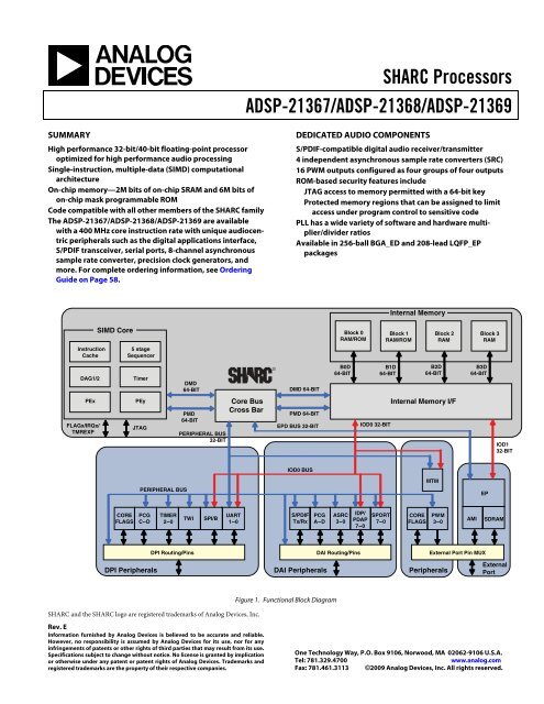
Figure 1. Functional Block Diagram<br />
DEDICATED AUDIO COMPONENTS<br />
S/PDIF-compatible digital audio receiver/transmitter<br />
4 independent asynchronous sample rate converters (SRC)<br />
16 PWM outputs configured as four groups of four outputs<br />
ROM-based security features include<br />
JTAG access to memory permitted with a 64-bit key<br />
Protected memory regions that can be assigned to limit<br />
access under program control to sensitive code<br />
PLL has a wide variety of software and hardware multiplier/divider<br />
ratios<br />
Available in 256-ball BGA_ED and 208-lead LQFP_EP<br />
packages<br />
DMD 64-BIT<br />
PMD 64-BIT<br />
EPD BUS 32-BIT<br />
IOD0 BUS<br />
S/PDIF<br />
Tx/Rx<br />
PCG<br />
A-D<br />
Block 0<br />
RAM/ROM<br />
B0D<br />
64-BIT<br />
ASRC<br />
3-0<br />
IDP/<br />
PDAP<br />
7-0<br />
DAI Routing/Pins<br />
IOD0 32-BIT<br />
SPORT<br />
7-0<br />
Block 1<br />
RAM/ROM<br />
B1D<br />
64-BIT<br />
Internal Memory<br />
Block 2<br />
RAM<br />
Internal Memory I/F<br />
CORE<br />
FLAGS<br />
B2D<br />
64-BIT<br />
DPI Peripherals DAI Peripherals Peripherals<br />
MTM<br />
PWM<br />
3-0<br />
B3D<br />
64-BIT<br />
Block 3<br />
RAM<br />
AMI SDRAM<br />
One Technology Way, P.O. Box 9106, Norwood, MA 02062-9106 U.S.A.<br />
Tel: 781.329.4700 www.analog.com<br />
Fax: 781.461.3113 ©2009 <strong>Analog</strong> <strong>Devices</strong>, Inc. All rights reserved.<br />
EP<br />
External Port Pin MUX<br />
IOD1<br />
32-BIT<br />
External<br />
Port
<strong>ADSP</strong>-21367/<strong>ADSP</strong>-21368/<strong>ADSP</strong>-21369<br />
TABLE OF CONTENTS<br />
Summary ............................................................... 1<br />
Dedicated Audio Components .................................... 1<br />
General Description ................................................. 3<br />
<strong>SHARC</strong> Family Core Architecture ............................ 4<br />
Family Peripheral Architecture ................................ 7<br />
I/O <strong>Processor</strong> Features ......................................... 10<br />
System Design .................................................... 10<br />
Development Tools ............................................. 11<br />
Additional Information ........................................ 12<br />
Pin Function Descriptions ....................................... 13<br />
Specifications ........................................................ 16<br />
Operating Conditions .......................................... 16<br />
Electrical Characteristics ....................................... 17<br />
Package Information ........................................... 18<br />
REVISION HISTORY<br />
7/09—Rev. D to Rev. E<br />
Corrected all outstanding document errata. Also replaced core<br />
clock references (CCLK) in the timing specifications with<br />
peripheral clock references (PCLK).<br />
Revised Functional Block Diagram ................................1<br />
Added Context Switch ...............................................5<br />
Added Universal Registers ..........................................5<br />
Clarified VCO operations. See<br />
Voltage Controlled Oscillator .................................... 18<br />
Corrected the pins names for the DAI and DPI in<br />
256-Ball BGA_ED Pinout ......................................... 51<br />
208-Lead LQFP_EP Pinout ....................................... 54<br />
Added 366 MHz LQFP EPAD models for the <strong>ADSP</strong>-21367 and<br />
<strong>ADSP</strong>-21369. For additional specifications for these models,<br />
refer to the following:<br />
Specifications ......................................................... 16<br />
Clock Input ........................................................... 21<br />
SDRAM Interface Timing (166 MHz SDCLK) ............... 28<br />
Serial Ports ............................................................ 34<br />
Ordering Guide ...................................................... 58<br />
Rev. E | Page 2 of 60 | July 2009<br />
ESD Caution ...................................................... 18<br />
Maximum Power Dissipation ................................. 18<br />
Absolute Maximum Ratings ................................... 18<br />
Timing Specifications ........................................... 18<br />
Output Drive Currents ......................................... 48<br />
Test Conditions .................................................. 48<br />
Capacitive Loading .............................................. 48<br />
Thermal Characteristics ........................................ 50<br />
256-Ball BGA_ED Pinout ......................................... 51<br />
208-Lead LQFP_EP Pinout ....................................... 54<br />
Package Dimensions ............................................... 56<br />
Surface-Mount Design .......................................... 57<br />
Automotive Products .............................................. 58<br />
Ordering Guide ..................................................... 58
GENERAL DESCRIPTION<br />
The <strong>ADSP</strong>-21367/<strong>ADSP</strong>-21368/<strong>ADSP</strong>-21369 <strong>SHARC</strong> ® processors<br />
are members of the SIMD <strong>SHARC</strong> family of DSPs that<br />
feature <strong>Analog</strong> <strong>Devices</strong>’ Super Harvard Architecture. These processors<br />
are source code-compatible with the <strong>ADSP</strong>-2126x and<br />
<strong>ADSP</strong>-2116x DSPs as well as with first generation <strong>ADSP</strong>-2106x<br />
<strong>SHARC</strong> processors in SISD (single-instruction, single-data)<br />
mode. The processors are 32-bit/40-bit floating-point processors<br />
optimized for high performance automotive audio<br />
applications with its large on-chip SRAM, mask programmable<br />
ROM, multiple internal buses to eliminate I/O bottlenecks, and<br />
an innovative digital applications interface (DAI).<br />
As shown in the functional block diagram on Page 1, the<br />
processors use two computational units to deliver a significant<br />
performance increase over the previous <strong>SHARC</strong> processors on a<br />
range of DSP algorithms. Fabricated in a state-of-the-art, high<br />
speed, CMOS process, the <strong>ADSP</strong>-21367/<strong>ADSP</strong>-21368/<br />
<strong>ADSP</strong>-21369 processors achieve an instruction cycle time of up<br />
to 2.5 ns at 400 MHz. With its SIMD computational hardware,<br />
the processors can perform 2.4 GFLOPS running at 400 MHz.<br />
Table 1 shows performance benchmarks for these devices.<br />
Table 1. <strong>Processor</strong> Benchmarks (at 400 MHz)<br />
Benchmark Algorithm<br />
Speed<br />
(at 400 MHz)<br />
1024 Point Complex FFT (Radix 4, with reversal) 23.2 μs<br />
FIR Filter (per tap) 1<br />
1.25 ns<br />
IIR Filter (per biquad) 1 Matrix Multiply (pipelined)<br />
5.0 ns<br />
[3×3] × [3×1]<br />
11.25 ns<br />
[4×4] × [4×1]<br />
20.0 ns<br />
Divide (y/x) 8.75 ns<br />
Inverse Square Root 13.5 ns<br />
1 Assumes two files in multichannel SIMD mode.<br />
Table 2. <strong>ADSP</strong>-2136x Family Features 1<br />
Feature <strong>ADSP</strong>-21367<br />
<strong>ADSP</strong>-21368<br />
Frequency 400 MHz<br />
RAM 2M bits<br />
ROM 2 6M bits<br />
Audio Decoders in ROM Yes<br />
Pulse-Width Modulation Yes<br />
S/PDIF Yes<br />
SDRAM Memory Bus Width 32/16 bits<br />
<strong>ADSP</strong>-21369/<br />
<strong>ADSP</strong>-21369W<br />
Rev. E | Page 3 of 60 | July 2009<br />
<strong>ADSP</strong>-21367/<strong>ADSP</strong>-21368/<strong>ADSP</strong>-21369<br />
Table 2. <strong>ADSP</strong>-2136x Family Features 1 (Continued)<br />
<strong>ADSP</strong>-21368<br />
<strong>ADSP</strong>-21369/<br />
<strong>ADSP</strong>-21369W<br />
<strong>ADSP</strong>-21367<br />
Feature<br />
Serial Ports 8<br />
IDP Yes<br />
DAI Yes<br />
UART 2<br />
DAI and DPI Yes<br />
S/PDIF Transceiver 1<br />
AMI Interface Bus Width 32/16/8 bits<br />
SPI 2<br />
TWI Yes<br />
SRC Performance 128 dB<br />
Package 256 Ball- 256 Ball- 256 Ball-<br />
BGA, BGA BGA,<br />
208-Lead<br />
208-Lead<br />
LQFP_EP<br />
LQFP_EP<br />
1 W = Automotive grade product. See Automotive Products on Page 58 for more<br />
information.<br />
2 Audio decoding algorithms include PCM, Dolby Digital EX, Dolby Prologic IIx,<br />
DTS 96/24, Neo:6, DTS ES, MPEG-2 AAC, MP3, and functions like bass<br />
management, delay, speaker equalization, graphic equalization, and more.<br />
Decoder/post-processor algorithm combination support varies depending upon<br />
the chip version and the system configurations. Please visit www.analog.com for<br />
complete information.<br />
The diagram on Page 1 shows the two clock domains that make<br />
up the <strong>ADSP</strong>-21367/<strong>ADSP</strong>-21368/<strong>ADSP</strong>-21369 processors. The<br />
core clock domain contains the following features.<br />
• Two processing elements (PEx, PEy), each of which comprises<br />
an ALU, multiplier, shifter, and data register file<br />
• <strong>Data</strong> address generators (DAG1, DAG2)<br />
• Program sequencer with instruction cache<br />
• PM and DM buses capable of supporting 2x64-bit data<br />
transfers between memory and the core at every core processor<br />
cycle<br />
• One periodic interval timer with pinout<br />
• On-chip SRAM (2M bit)<br />
• On-chip mask-programmable ROM (6M bit)<br />
• JTAG test access port for emulation and boundary scan.<br />
The JTAG provides software debug through user breakpoints<br />
which allows flexible exception handling.
<strong>ADSP</strong>-21367/<strong>ADSP</strong>-21368/<strong>ADSP</strong>-21369<br />
The block diagram of the <strong>ADSP</strong>-21368 on Page 1 also shows the<br />
peripheral clock domain (also known as the I/O processor) and<br />
contains the following features:<br />
• IOD0 (peripheral DMA) and IOD1 (external port DMA)<br />
buses for 32-bit data transfers<br />
• Peripheral and external port buses for core connection<br />
• External port with an AMI and SDRAM controller<br />
• 4 units for PWM control<br />
• 1 MTM unit for internal-to-internal memory transfers<br />
• Digital applications interface that includes four precision<br />
clock generators (PCG), a input data port (IDP) for serial<br />
and parallel interconnect, an S/PDIF receiver/transmitter,<br />
four asynchronous sample rate converters, eight serial<br />
ports, a flexible signal routing unit (DAI SRU).<br />
S<br />
SIMD Core<br />
MRF<br />
80-BIT<br />
DAG1<br />
16x32<br />
DMD/PMD 64<br />
MULTIPLIER SHIFTER<br />
MRB<br />
80-BIT<br />
DAG2<br />
16x32<br />
ALU<br />
JTAG<br />
FLAG<br />
RF<br />
Rx/Fx<br />
PEx<br />
16x40-BIT<br />
ASTATx<br />
STYKx<br />
5 STAGE<br />
PROGRAM SEQUENCER<br />
Figure 2. <strong>SHARC</strong> Core Block Diadram<br />
Rev. E | Page 4 of 60 | July 2009<br />
• Digital peripheral interface that includes three timers, a 2-<br />
wire interface, two UARTs, two serial peripheral interfaces<br />
(SPI), 2 precision clock generators (PCG) and a flexible signal<br />
routing unit (DPI SRU).<br />
<strong>SHARC</strong> FAMILY CORE ARCHITECTURE<br />
The <strong>ADSP</strong>-21367/<strong>ADSP</strong>-21368/<strong>ADSP</strong>-21369 are code compatible<br />
at the assembly level with the <strong>ADSP</strong>-2126x, <strong>ADSP</strong>-21160,<br />
and <strong>ADSP</strong>-21161, and with the first generation <strong>ADSP</strong>-2106x<br />
<strong>SHARC</strong> processors. The <strong>ADSP</strong>-21367/<strong>ADSP</strong>-21368/<br />
<strong>ADSP</strong>-21369 processors share architectural features with the<br />
<strong>ADSP</strong>-2126x and <strong>ADSP</strong>-2116x SIMD <strong>SHARC</strong> processors, as<br />
shown in Figure 2 and detailed in the following sections.<br />
TIMER INTERRUPT CACHE<br />
DATA<br />
SWAP<br />
RF<br />
Sx/SFx<br />
PEy<br />
16x40-BIT<br />
ASTATy<br />
STYKy<br />
PM ADDRESS 32<br />
DM ADDRESS 32<br />
PM DATA 64<br />
DM DATA 64<br />
PM DATA 48<br />
PM ADDRESS 24<br />
MSB<br />
80-BIT<br />
SYSTEM<br />
I/F<br />
USTAT<br />
4x32-BIT<br />
PX<br />
64-BIT<br />
ALU SHIFTER MULTIPLIER<br />
MSF<br />
80-BIT
SIMD Computational Engine<br />
The processors contain two computational processing elements<br />
that operate as a single-instruction, multiple-data (SIMD)<br />
engine. The processing elements are referred to as PEX and PEY<br />
and each contains an ALU, multiplier, shifter, and register file.<br />
PEX is always active, and PEY may be enabled by setting the<br />
PEYEN mode bit in the MODE1 register. When this mode is<br />
enabled, the same instruction is executed in both processing elements,<br />
but each processing element operates on different data.<br />
This architecture is efficient at executing math intensive DSP<br />
algorithms.<br />
Entering SIMD mode also has an effect on the way data is transferred<br />
between memory and the processing elements. When in<br />
SIMD mode, twice the data bandwidth is required to sustain<br />
computational operation in the processing elements. Because of<br />
this requirement, entering SIMD mode also doubles the bandwidth<br />
between memory and the processing elements. When<br />
using the DAGs to transfer data in SIMD mode, two data values<br />
are transferred with each access of memory or the register file.<br />
Independent, Parallel Computation Units<br />
Within each processing element is a set of computational units.<br />
The computational units consist of an arithmetic/logic unit<br />
(ALU), multiplier, and shifter. These units perform all operations<br />
in a single cycle. The three units within each processing<br />
element are arranged in parallel, maximizing computational<br />
throughput. Single multifunction instructions execute parallel<br />
ALU and multiplier operations. In SIMD mode, the parallel<br />
ALU and multiplier operations occur in both processing<br />
elements. These computation units support IEEE 32-bit singleprecision<br />
floating-point, 40-bit extended precision floatingpoint,<br />
and 32-bit fixed-point data formats.<br />
<strong>Data</strong> Register File<br />
A general-purpose data register file is contained in each processing<br />
element. The register files transfer data between the<br />
computation units and the data buses, and store intermediate<br />
results. These 10-port, 32-register (16 primary, 16 secondary)<br />
register files, combined with the <strong>ADSP</strong>-2136x enhanced Harvard<br />
architecture, allow unconstrained data flow between<br />
computation units and internal memory. The registers in PEX<br />
are referred to as R0–R15 and in PEY as S0–S15.<br />
Context Switch<br />
Many of the processor’s registers have secondary registers that<br />
can be activated during interrupt servicing for a fast context<br />
switch. The data registers in the register file, the DAG registers,<br />
and the multiplier result registers all have secondary registers.<br />
The primary registers are active at reset, while the secondary<br />
registers are activated by control bits in a mode control register.<br />
Universal Registers<br />
These registers can be used for general-purpose tasks. The<br />
USTAT (4) registers allow easy bit manipulations (Set, Clear,<br />
Toggle, Test, XOR) for all system registers (control/status) of<br />
the core.<br />
Rev. E | Page 5 of 60 | July 2009<br />
<strong>ADSP</strong>-21367/<strong>ADSP</strong>-21368/<strong>ADSP</strong>-21369<br />
The data bus exchange register (PX) permits data to be passed<br />
between the 64-bit PM data bus and the 64-bit DM data bus, or<br />
between the 40-bit register file and the PM data bus. These registers<br />
contain hardware to handle the data width difference.<br />
Timer<br />
A core timer that can generate periodic software Interrupts. The<br />
core timer can be configured to use FLAG3 as a timer expired<br />
signal<br />
Single-Cycle Fetch of Instruction and Four Operands<br />
The <strong>ADSP</strong>-21367/<strong>ADSP</strong>-21368/<strong>ADSP</strong>-21369 feature an<br />
enhanced Harvard architecture in which the data memory<br />
(DM) bus transfers data and the program memory (PM) bus<br />
transfers both instructions and data (see Figure 2 on Page 4).<br />
With separate program and data memory buses and on-chip<br />
instruction cache, the processors can simultaneously fetch four<br />
operands (two over each data bus) and one instruction (from<br />
the cache), all in a single cycle.<br />
Instruction Cache<br />
The processors include an on-chip instruction cache that<br />
enables three-bus operation for fetching an instruction and four<br />
data values. The cache is selective—only the instructions whose<br />
fetches conflict with PM bus data accesses are cached. This<br />
cache allows full-speed execution of core, looped operations<br />
such as digital filter multiply-accumulates, and FFT butterfly<br />
processing.<br />
<strong>Data</strong> Address Generators with Zero-Overhead Hardware<br />
Circular Buffer Support<br />
The <strong>ADSP</strong>-21367/<strong>ADSP</strong>-21368/<strong>ADSP</strong>-21369 have two data<br />
address generators (DAGs). The DAGs are used for indirect<br />
addressing and implementing circular data buffers in hardware.<br />
Circular buffers allow efficient programming of delay lines and<br />
other data structures required in digital signal processing, and<br />
are commonly used in digital filters and Fourier transforms.<br />
The two DAGs contain sufficient registers to allow the creation<br />
of up to 32 circular buffers (16 primary register sets, 16 secondary).<br />
The DAGs automatically handle address pointer<br />
wraparound, reduce overhead, increase performance, and simplify<br />
implementation. Circular buffers can start and end at any<br />
memory location.<br />
Flexible Instruction Set<br />
The 48-bit instruction word accommodates a variety of parallel<br />
operations for concise programming. For example, the<br />
<strong>ADSP</strong>-21367/<strong>ADSP</strong>-21368/<strong>ADSP</strong>-21369 can conditionally execute<br />
a multiply, an add, and a subtract in both processing<br />
elements while branching and fetching up to four 32-bit values<br />
from memory—all in a single instruction.<br />
On-Chip Memory<br />
The processors contain two megabits of internal RAM and six<br />
megabits of internal mask-programmable ROM. Each block can<br />
be configured for different combinations of code and data storage<br />
(see Table 3 on Page 6). Each memory block supports<br />
single-cycle, independent accesses by the core processor and I/O
<strong>ADSP</strong>-21367/<strong>ADSP</strong>-21368/<strong>ADSP</strong>-21369<br />
processor. The memory architecture, in combination with its<br />
separate on-chip buses, allows two data transfers from the core<br />
and one from the I/O processor, in a single cycle.<br />
Table 3. Internal Memory Space 1<br />
IOP Registers 0x0000 0000–0x0003 FFFF<br />
Extended Precision Normal or<br />
Long Word (64 Bits)<br />
Instruction Word (48 Bits) Normal Word (32 Bits) Short Word (16 Bits)<br />
Block 0 ROM (Reserved)<br />
0x0004 0000–0x0004 BFFF<br />
Reserved<br />
0x0004 F000–0x0004 FFFF<br />
Block 0 SRAM<br />
0x0004 C000–0x0004 EFFF<br />
Block 1 ROM (Reserved)<br />
0x0005 0000–0x0005 BFFF<br />
Reserved<br />
0x0005 F000–0x0005 FFFF<br />
Block 1 SRAM<br />
0x0005 C000–0x0005 EFFF<br />
Block 2 SRAM<br />
0x0006 0000–0x0006 0FFF<br />
Reserved<br />
0x0006 1000– 0x0006 FFFF<br />
Block 3 SRAM<br />
0x0007 0000–0x0007 0FFF<br />
Reserved<br />
0x0007 1000–0x0007 FFFF<br />
Block 0 ROM (Reserved)<br />
0x0008 0000–0x0008 FFFF<br />
Reserved<br />
0x0009 4000–0x0009 FFFF<br />
Block 0 SRAM<br />
0x0009 0000–0x0009 3FFF<br />
Block 1 ROM (Reserved)<br />
0x000A 0000–0x000A FFFF<br />
Reserved<br />
0x000B 4000–0x000B FFFF<br />
Block 1 SRAM<br />
0x000B 0000–0x000B 3FFF<br />
Block 2 SRAM<br />
0x000C 0000–0x000C 1554<br />
Reserved<br />
0x000C 1555–0x000C 3FFF<br />
Block 3 SRAM<br />
0x000E 0000–0x000E 1554<br />
Reserved<br />
0x000E 1555–0x000F FFFF<br />
The SRAM can be configured as a maximum of 64k words of<br />
32-bit data, 128k words of 16-bit data, 42k words of 48-bit<br />
instructions (or 40-bit data), or combinations of different word<br />
sizes up to two megabits. All of the memory can be accessed as<br />
16-bit, 32-bit, 48-bit, or 64-bit words. A 16-bit floating-point<br />
storage format is supported that effectively doubles the amount<br />
of data that can be stored on-chip. Conversion between the<br />
32-bit floating-point and 16-bit floating-point formats is performed<br />
in a single instruction. While each memory block can<br />
store combinations of code and data, accesses are most efficient<br />
when one block stores data using the DM bus for transfers, and<br />
the other block stores instructions and data using the PM bus<br />
for transfers.<br />
Using the DM bus and PM buses, with one bus dedicated to<br />
each memory block, assures single-cycle execution with two<br />
data transfers. In this case, the instruction must be available in<br />
the cache.<br />
Block 0 ROM (Reserved)<br />
0x0008 0000–0x0009 7FFF<br />
Reserved<br />
0x0009 E000–0x0009 FFFF<br />
Block 0 SRAM<br />
0x0009 8000–0x0009 DFFF<br />
Block 1 ROM (Reserved)<br />
0x000A 0000–0x000B 7FFF<br />
Reserved<br />
0x000B E000–0x000B FFFF<br />
Block 1 SRAM<br />
0x000B 8000–0x000B DFFF<br />
Block 2 SRAM<br />
0x000C 0000–0x000C 1FFF<br />
Reserved<br />
0x000C 2000–0x000D FFFF<br />
Block 3 SRAM<br />
0x000E 0000–0x000E 1FFF<br />
Reserved<br />
0x000E 2000–0x000F FFFF<br />
Rev. E | Page 6 of 60 | July 2009<br />
Block 0 ROM (Reserved)<br />
0x0010 0000–0x0012 FFFF<br />
Reserved<br />
0x0013 C000–0x0013 FFFF<br />
Block 0 SRAM<br />
0x0013 0000–0x0013 BFFF<br />
Block 1 ROM (Reserved)<br />
0x0014 0000–0x0016 FFFF<br />
Reserved<br />
0x0017 C000–0x0017 FFFF<br />
Block 1 SRAM<br />
0x0017 0000–0x0017 BFFF<br />
Block 2 SRAM<br />
0x0018 0000–0x0018 3FFF<br />
Reserved<br />
0x0018 4000–0x001B FFFF<br />
Block 3 SRAM<br />
0x001C 0000–0x001C 3FFF<br />
Reserved<br />
0x001C 4000–0x001F FFFF<br />
1 The <strong>ADSP</strong>-21368 and <strong>ADSP</strong>-21369 processors include a customer-definable ROM block. Please contact your <strong>Analog</strong> <strong>Devices</strong> sales representative for additional details.<br />
On-Chip Memory Bandwidth<br />
The internal memory architecture allows programs to have four<br />
accesses at the same time to any of the four blocks (assuming<br />
there are no block conflicts). The total bandwidth is realized<br />
using the DMD and PMD buses (2x64-bits, core CLK) and the<br />
IOD0/1 buses (2x32-bit, PCLK).<br />
ROM-Based Security<br />
The <strong>ADSP</strong>-21367/<strong>ADSP</strong>-21368/<strong>ADSP</strong>-21369 have a ROM security<br />
feature that provides hardware support for securing user<br />
software code by preventing unauthorized reading from the<br />
internal code when enabled. When using this feature, the processor<br />
does not boot-load any external code, executing<br />
exclusively from internal ROM. Additionally, the processor is<br />
not freely accessible via the JTAG port. Instead, a unique 64-bit<br />
key, which must be scanned in through the JTAG or test access<br />
port will be assigned to each customer. The device will ignore a<br />
wrong key. Emulation features and external boot modes are<br />
only available after the correct key is scanned.
FAMILY PERIPHERAL ARCHITECTURE<br />
The <strong>ADSP</strong>-21367/<strong>ADSP</strong>-21368/<strong>ADSP</strong>-21369 family contains a<br />
rich set of peripherals that support a wide variety of applications<br />
including high quality audio, medical imaging, communications,<br />
military, test equipment, 3D graphics, speech recognition,<br />
motor control, imaging, and other applications.<br />
External Port<br />
The external port interface supports access to the external memory<br />
through core and DMA accesses. The external memory<br />
address space is divided into four banks. Any bank can be programmed<br />
as either asynchronous or synchronous memory. The<br />
external ports of the <strong>ADSP</strong>-21367/8/9 processors are comprised<br />
of the following modules.<br />
• An Asynchronous Memory Interface which communicates<br />
with SRAM, FLASH, and other devices that meet the standard<br />
asynchronous SRAM access protocol. The AMI<br />
supports 14M words of external memory in bank 0 and<br />
16M words of external memory in bank 1, bank 2, and<br />
bank 3.<br />
• An SDRAM controller that supports a glueless interface<br />
with any of the standard SDRAMs. The SDC supports 62M<br />
words of external memory in bank 0, and 64M words of<br />
external memory in bank 1, bank 2, and bank 3.<br />
• Arbitration Logic to coordinate core and DMA transfers<br />
between internal and external memory over the external<br />
port.<br />
• A Shared Memory Interface that allows the connection of<br />
up to four <strong>ADSP</strong>-21368 processors to create shared external<br />
bus systems (<strong>ADSP</strong>-21368 only).<br />
SDRAM Controller<br />
The SDRAM controller provides an interface of up to four separate<br />
banks of industry-standard SDRAM devices or DIMMs, at<br />
speeds up to fSCLK. Fully compliant with the SDRAM standard,<br />
each bank has its own memory select line (MS0–MS3), and can<br />
be configured to contain between 16M bytes and 128M bytes of<br />
memory. SDRAM external memory address space is shown in<br />
Table 4.<br />
A set of programmable timing parameters is available to configure<br />
the SDRAM banks to support slower memory devices. The<br />
memory banks can be configured as either 32 bits wide for maximum<br />
performance and bandwidth or 16 bits wide for<br />
minimum device count and lower system cost.<br />
The SDRAM controller address, data, clock, and control pins<br />
can drive loads up to distributed 30 pF loads. For larger memory<br />
systems, the SDRAM controller external buffer timing should<br />
be selected and external buffering should be provided so that the<br />
load on the SDRAM controller pins does not exceed 30 pF.<br />
External Memory<br />
The external port provides a high performance, glueless interface<br />
to a wide variety of industry-standard memory devices. The<br />
32-bit wide bus can be used to interface to synchronous and/or<br />
asynchronous memory devices through the use of its separate<br />
internal memory controllers. The first is an SDRAM controller<br />
Rev. E | Page 7 of 60 | July 2009<br />
<strong>ADSP</strong>-21367/<strong>ADSP</strong>-21368/<strong>ADSP</strong>-21369<br />
Table 4. External Memory for SDRAM Addresses<br />
Bank<br />
Size in<br />
Words Address Range<br />
Bank 0 62M 0x0020 0000–0x03FF FFFF<br />
Bank 1 64M 0x0400 0000–0x07FF FFFF<br />
Bank 2 64M 0x0800 0000–0x0BFF FFFF<br />
Bank 3 64M 0x0C00 0000–0x0FFF FFFF<br />
for connection of industry-standard synchronous DRAM<br />
devices and DIMMs (dual inline memory module), while the<br />
second is an asynchronous memory controller intended to<br />
interface to a variety of memory devices. Four memory select<br />
pins enable up to four separate devices to coexist, supporting<br />
any desired combination of synchronous and asynchronous<br />
device types. Non-SDRAM external memory address space is<br />
shown in Table 5.<br />
Table 5. External Memory for Non-SDRAM Addresses<br />
Bank<br />
Size in<br />
Words Address Range<br />
Bank 0 14M 0x0020 0000–0x00FF FFFF<br />
Bank 1 16M 0x0400 0000–0x04FF FFFF<br />
Bank 2 16M 0x0800 0000–0x08FF FFFF<br />
Bank 3 16M 0x0C00 0000–0x0CFF FFFF<br />
Shared External Memory<br />
The <strong>ADSP</strong>-21368 processor supports connecting to common<br />
shared external memory with other <strong>ADSP</strong>-21368 processors to<br />
create shared external bus processor systems. This support<br />
includes:<br />
• Distributed, on-chip arbitration for the shared external bus<br />
• Fixed and rotating priority bus arbitration<br />
• Bus time-out logic<br />
• Bus lock<br />
Multiple processors can share the external bus with no additional<br />
arbitration logic. Arbitration logic is included on-chip to<br />
allow the connection of up to four processors.<br />
Bus arbitration is accomplished through the BR1–4 signals and<br />
the priority scheme for bus arbitration is determined by the setting<br />
of the RPBA pin. Table 8 on Page 13 provides descriptions<br />
of the pins used in multiprocessor systems.<br />
External Port Throughput<br />
The throughput for the external port, based on 166 MHz clock<br />
and 32-bit data bus, is 221M bytes/s for the AMI and 664M<br />
bytes/s for SDRAM.
<strong>ADSP</strong>-21367/<strong>ADSP</strong>-21368/<strong>ADSP</strong>-21369<br />
Asynchronous Memory Controller<br />
The asynchronous memory controller provides a configurable<br />
interface for up to four separate banks of memory or I/O<br />
devices. Each bank can be independently programmed with different<br />
timing parameters, enabling connection to a wide variety<br />
of memory devices including SRAM, ROM, flash, and EPROM,<br />
as well as I/O devices that interface with standard memory<br />
control lines. Bank 0 occupies a 14M word window and Banks 1,<br />
2, and 3 occupy a 16M word window in the processor’s address<br />
space but, if not fully populated, these windows are not made<br />
contiguous by the memory controller logic. The banks can also<br />
be configured as 8-bit, 16-bit, or 32-bit wide buses for ease of<br />
interfacing to a range of memories and I/O devices tailored<br />
either to high performance or to low cost and power.<br />
Pulse-Width Modulation<br />
The PWM module is a flexible, programmable, PWM waveform<br />
generator that can be programmed to generate the required<br />
switching patterns for various applications related to motor and<br />
engine control or audio power control. The PWM generator can<br />
generate either center-aligned or edge-aligned PWM waveforms.<br />
In addition, it can generate complementary signals on<br />
two outputs in paired mode or independent signals in nonpaired<br />
mode (applicable to a single group of four PWM<br />
waveforms).<br />
The entire PWM module has four groups of four PWM outputs<br />
each. Therefore, this module generates 16 PWM outputs in<br />
total. Each PWM group produces two pairs of PWM signals on<br />
the four PWM outputs.<br />
The PWM generator is capable of operating in two distinct<br />
modes while generating center-aligned PWM waveforms: single<br />
update mode or double update mode. In single update mode,<br />
the duty cycle values are programmable only once per PWM<br />
period. This results in PWM patterns that are symmetrical<br />
about the midpoint of the PWM period. In double update<br />
mode, a second updating of the PWM registers is implemented<br />
at the midpoint of the PWM period. In this mode, it is possible<br />
to produce asymmetrical PWM patterns that produce lower<br />
harmonic distortion in 2-phase PWM inverters.<br />
Digital Applications Interface (DAI)<br />
The digital applications interface (DAI ) provide the ability to<br />
connect various peripherals to any of the DSP’s DAI pins<br />
(DAI_P20–1). Programs make these connections using the signal<br />
routing unit (SRU1), shown in Figure 1.<br />
The SRU is amatrix routing unit (or group of multiplexers) that<br />
enable the peripherals provided by the DAI to be interconnected<br />
under software control. This allows easy use of the<br />
associated peripherals for a much wider variety of applications<br />
by using a larger set of algorithms than is possible with nonconfigurable<br />
signal paths.<br />
The DAI include eight serial ports, an S/PDIF receiver/transmitter,<br />
four precision clock generators (PCG), eight channels of<br />
synchronous sample rate converters, and an input data port<br />
(IDP). The IDP provides an additional input path to the<br />
Rev. E | Page 8 of 60 | July 2009<br />
processor core, configurable as either eight channels of I2S serial<br />
data or as seven channels plus a single 20-bit wide synchronous<br />
parallel data acquisition port. Each data channel has its own<br />
DMA channel that is independent from the processor’s serial<br />
ports.<br />
For complete information on using the DAI, see the<br />
<strong>ADSP</strong>-21368 <strong>SHARC</strong> <strong>Processor</strong> Hardware Reference.<br />
Serial Ports<br />
The processors feature eight synchronous serial ports (SPORTs)<br />
that provide an inexpensive interface to a wide variety of digital<br />
and mixed-signal peripheral devices such as <strong>Analog</strong> <strong>Devices</strong>’<br />
AD183x family of audio codecs, ADCs, and DACs. The serial<br />
ports are made up of two data lines, a clock, and frame sync. The<br />
data lines can be programmed to either transmit or receive and<br />
each data line has a dedicated DMA channel.<br />
Serial ports are enabled via 16 programmable and simultaneous<br />
receive or transmit pins that support up to 32 transmit or 32<br />
receive channels of audio data when all eight SPORTs are<br />
enabled, or eight full duplex TDM streams of 128 channels<br />
per frame.<br />
The serial ports operate at a maximum data rate of 50 Mbps.<br />
Serial port data can be automatically transferred to and from<br />
on-chip memory via dedicated DMA channels. Each of the<br />
serial ports can work in conjunction with another serial port to<br />
provide TDM support. One SPORT provides two transmit signals<br />
while the other SPORT provides the two receive signals.<br />
The frame sync and clock are shared.<br />
Serial ports operate in five modes:<br />
• Standard DSP serial mode<br />
• Multichannel (TDM) mode with support for packed I2S mode<br />
• I2S mode<br />
• Packed I2S mode<br />
• Left-justified sample pair mode<br />
Left-justified sample pair mode is a mode where in each frame<br />
sync cycle two samples of data are transmitted/received—one<br />
sample on the high segment of the frame sync, the other on the<br />
low segment of the frame sync. Programs have control over various<br />
attributes of this mode.<br />
Each of the serial ports supports the left-justified sample pair<br />
and I2S protocols (I2S is an industry-standard interface commonly<br />
used by audio codecs, ADCs, and DACs such as the<br />
<strong>Analog</strong> <strong>Devices</strong> AD183x family), with two data pins, allowing<br />
four left-justified sample pair or I2S channels (using two stereo<br />
devices) per serial port, with a maximum of up to 32 I2S channels.<br />
The serial ports permit little-endian or big-endian<br />
transmission formats and word lengths selectable from 3 bits to<br />
32 bits. For the left-justified sample pair and I2S modes, dataword<br />
lengths are selectable between 8 bits and 32 bits. Serial<br />
ports offer selectable synchronization and transmit modes as<br />
well as optional μ-law or A-law companding selection on a per<br />
channel basis. Serial port clocks and frame syncs can be internally<br />
or externally generated.
The serial ports also contain frame sync error detection logic<br />
where the serial ports detect frame syncs that arrive early (for<br />
example, frame syncs that arrive while the transmission/reception<br />
of the previous word is occurring). All the serial ports also<br />
share one dedicated error interrupt.<br />
S/PDIF-Compatible Digital Audio Receiver/Transmitter<br />
The S/PDIF receiver/transmitter has no separate DMA channels.<br />
It receives audio data in serial format and converts it into a<br />
biphase encoded signal. The serial data input to the<br />
receiver/transmitter can be formatted as left-justified, I2S, or<br />
right-justified with word widths of 16, 18, 20, or 24 bits.<br />
The serial data, clock, and frame sync inputs to the S/PDIF<br />
receiver/transmitter are routed through the signal routing unit<br />
(SRU). They can come from a variety of sources such as the<br />
SPORTs, external pins, the precision clock generators (PCGs),<br />
or the sample rate converters (SRC) and are controlled by the<br />
SRU control registers.<br />
Synchronous/Asynchronous Sample Rate Converter<br />
The sample rate converter (SRC) contains four SRC blocks and<br />
is the same core as that used in the AD1896 192 kHz stereo<br />
asynchronous sample rate converter and provides up to 128 dB<br />
SNR. The SRC block is used to perform synchronous or asynchronous<br />
sample rate conversion across independent stereo<br />
channels, without using internal processor resources. The four<br />
SRC blocks can also be configured to operate together to convert<br />
multichannel audio data without phase mismatches.<br />
<strong>Final</strong>ly, the SRC can be used to clean up audio data from jittery<br />
clock sources such as the S/PDIF receiver.<br />
Input <strong>Data</strong> Port<br />
The IDP provides up to eight serial input channels—each with<br />
its own clock, frame sync, and data inputs. The eight channels<br />
are automatically multiplexed into a single 32-bit by eight-deep<br />
FIFO. <strong>Data</strong> is always formatted as a 64-bit frame and divided<br />
into two 32-bit words. The serial protocol is designed to receive<br />
audio channels in I2S, left-justified sample pair, or right-justified<br />
mode. One frame sync cycle indicates one 64-bit left/right<br />
pair, but data is sent to the FIFO as 32-bit words (that is, onehalf<br />
of a frame at a time). The processor supports 24- and 32-bit<br />
I2S, 24- and 32-bit left-justified, and 24-, 20-, 18- and 16-bit<br />
right-justified formats.<br />
Precision Clock Generators<br />
The precision clock generators (PCG) consist of four units, each<br />
of which generates a pair of signals (clock and frame sync)<br />
derived from a clock input signal. The units, A B, C, and D, are<br />
identical in functionality and operate independently of each<br />
other. The two signals generated by each unit are normally used<br />
as a serial bit clock/frame sync pair.<br />
Digital Peripheral Interface (DPI)<br />
The digital peripheral interface provides connections to two<br />
serial peripheral interface ports (SPI), two universal asynchronous<br />
receiver-transmitters (UARTs), a 2-wire interface (TWI),<br />
12 flags, and three general-purpose timers.<br />
Rev. E | Page 9 of 60 | July 2009<br />
<strong>ADSP</strong>-21367/<strong>ADSP</strong>-21368/<strong>ADSP</strong>-21369<br />
Serial Peripheral (Compatible) Interface<br />
The processors contain two serial peripheral interface ports<br />
(SPIs). The SPI is an industry-standard synchronous serial link,<br />
enabling the SPI-compatible port to communicate with other<br />
SPI-compatible devices. The SPI consists of two data pins, one<br />
device select pin, and one clock pin. It is a full-duplex<br />
synchronous serial interface, supporting both master and slave<br />
modes. The SPI port can operate in a multimaster environment<br />
by interfacing with up to four other SPI-compatible devices,<br />
either acting as a master or slave device. The <strong>ADSP</strong>-21367/<br />
<strong>ADSP</strong>-21368/<strong>ADSP</strong>-21369 SPI-compatible peripheral implementation<br />
also features programmable baud rate and clock<br />
phase and polarities. The SPI-compatible port uses open-drain<br />
drivers to support a multimaster configuration and to avoid<br />
data contention.<br />
UART Port<br />
The processors provide a full-duplex universal asynchronous<br />
receiver/transmitter (UART) port, which is fully compatible<br />
with PC-standard UARTs. The UART port provides a simplified<br />
UART interface to other peripherals or hosts, supporting<br />
full-duplex, DMA-supported, asynchronous transfers of serial<br />
data. The UART also has multiprocessor communication capability<br />
using 9-bit address detection. This allows it to be used in<br />
multidrop networks through the RS-485 data interface<br />
standard. The UART port also includes support for five data bits<br />
to eight data bits, one stop bit or two stop bits, and none, even,<br />
or odd parity. The UART port supports two modes of<br />
operation:<br />
• PIO (programmed I/O) – The processor sends or receives<br />
data by writing or reading I/O-mapped UART registers.<br />
The data is double-buffered on both transmit and receive.<br />
• DMA (direct memory access) – The DMA controller transfers<br />
both transmit and receive data. This reduces the<br />
number and frequency of interrupts required to transfer<br />
data to and from memory. The UART has two dedicated<br />
DMA channels, one for transmit and one for receive. These<br />
DMA channels have lower default priority than most DMA<br />
channels because of their relatively low service rates.<br />
The UART port’s baud rate, serial data format, error code generation<br />
and status, and interrupts are programmable:<br />
• Supporting bit rates ranging from (fSCLK/1,048,576) to<br />
(fSCLK/16) bits per second.<br />
• Supporting data formats from 7 bits to 12 bits per frame.<br />
• Both transmit and receive operations can be configured to<br />
generate maskable interrupts to the processor.<br />
Where the 16-bit UART_Divisor comes from the DLH register<br />
(most significant eight bits) and DLL register (least significant<br />
eight bits).<br />
In conjunction with the general-purpose timer functions, autobaud<br />
detection is supported.
<strong>ADSP</strong>-21367/<strong>ADSP</strong>-21368/<strong>ADSP</strong>-21369<br />
Peripheral Timers<br />
Three general-purpose timers can generate periodic interrupts<br />
and be independently set to operate in one of three modes:<br />
• Pulse waveform generation mode<br />
• Pulse width count/capture mode<br />
• External event watchdog mode<br />
Each general-purpose timer has one bidirectional pin and four<br />
registers that implement its mode of operation: a 6-bit configuration<br />
register, a 32-bit count register, a 32-bit period register,<br />
and a 32-bit pulse width register. A single control and status<br />
register enables or disables all three general-purpose timers<br />
independently.<br />
2-Wire Interface Port (TWI)<br />
The TWI is a bidirectional 2-wire serial bus used to move 8-bit<br />
data while maintaining compliance with the I2C bus protocol.<br />
The TWI master incorporates the following features:<br />
• Simultaneous master and slave operation on multiple<br />
device systems with support for multimaster data<br />
arbitration<br />
• Digital filtering and timed event processing<br />
• 7-bit and 10-bit addressing<br />
• 100 kbps and 400 kbps data rates<br />
• Low interrupt rate<br />
I/O PROCESSOR FEATURES<br />
The I/O processor provides many channels of DMA, and controls<br />
the extensive set of peripherals described in the previous<br />
sections.<br />
DMA Controller<br />
The processor’s on-chip DMA controller allows data transfers<br />
without processor intervention. The DMA controller operates<br />
independently and invisibly to the processor core, allowing<br />
DMA operations to occur while the core is simultaneously executing<br />
its program instructions. DMA transfers can occur<br />
between the processor’s internal memory and its serial ports, the<br />
SPI-compatible (serial peripheral interface) ports, the IDP<br />
(input data port), the parallel data acquisition port (PDAP), or<br />
the UART.<br />
Thirty four channels of DMA are available on the <strong>ADSP</strong>-2136x<br />
processors as shown in Table 6.<br />
Table 6. DMA Channels<br />
Peripheral DMA Channels<br />
SPORTs 16<br />
PDAP 8<br />
SPI 2<br />
UART 4<br />
External Port 2<br />
Memory-to-Memory 2<br />
Rev. E | Page 10 of 60 | July 2009<br />
Delay Line DMA<br />
The <strong>ADSP</strong>-21367/<strong>ADSP</strong>-21368/<strong>ADSP</strong>-21369 processors provide<br />
delay line DMA functionality. This allows processor reads<br />
and writes to external delay line buffers (in external memory,<br />
SRAM, or SDRAM) with limited core interaction.<br />
SYSTEM DESIGN<br />
The following sections provide an introduction to system design<br />
options and power supply issues.<br />
Program Booting<br />
The internal memory of the processors can be booted up at system<br />
power-up from an 8-bit EPROM via the external port, an<br />
SPI master or slave, or an internal boot. Booting is determined<br />
by the boot configuration (BOOT_CFG1–0) pins (see Table 7<br />
and the processor hardware reference). Selection of the boot<br />
source is controlled via the SPI as either a master or slave device,<br />
or it can immediately begin executing from ROM.<br />
Table 7. Boot Mode Selection<br />
BOOT_CFG1–0 Booting Mode<br />
00 SPI Slave Boot<br />
01 SPI Master Boot<br />
10 EPROM/FLASH Boot<br />
11 Reserved<br />
Power Supplies<br />
The processors have separate power supply connections for the<br />
internal (VDDINT), external (VDDEXT), and analog (AVDD/AVSS) power<br />
supplies. The internal and analog supplies must meet the 1.3 V<br />
requirement for the 400 MHz device and 1.2 V for the<br />
333 MHz and 266 MHz devices. The external supply must meet<br />
the 3.3 V requirement. All external supply pins must be connected<br />
to the same power supply.<br />
Note that the analog supply pin (AVDD) powers the processor’s<br />
internal clock generator PLL. To produce a stable clock, it is recommended<br />
that PCB designs use an external filter circuit for the<br />
AVDD pin. Place the filter components as close as possible to the<br />
AVDD/AVSS pins. For an example circuit, see Figure 3. (A recommended<br />
ferrite chip is the muRata BLM18AG102SN1D). To<br />
reduce noise coupling, the PCB should use a parallel pair of<br />
power and ground planes for VDDINT and GND. Use wide traces<br />
to connect the bypass capacitors to the analog power (AVDD) and<br />
ground (AVSS) pins. Note that the AVDD and AVSS pins specified in<br />
Figure 3 are inputs to the processor and not the analog ground<br />
plane on the board—the AVSS pin should connect directly to digital<br />
ground (GND) at the chip.
V DDINT<br />
HI-Z FERRITE<br />
BEAD CHIP<br />
Target Board JTAG Emulator Connector<br />
<strong>Analog</strong> <strong>Devices</strong> DSP Tools product line of JTAG emulators uses<br />
the IEEE 1149.1 JTAG test access port of the <strong>ADSP</strong>-21367/<br />
<strong>ADSP</strong>-21368/<strong>ADSP</strong>-21369 processors to monitor and control<br />
the target board processor during emulation. <strong>Analog</strong> <strong>Devices</strong><br />
DSP Tools product line of JTAG emulators provides emulation<br />
at full processor speed, allowing inspection and modification of<br />
memory, registers, and processor stacks. The processor’s JTAG<br />
interface ensures that the emulator will not affect target system<br />
loading or timing.<br />
For complete information on <strong>Analog</strong> <strong>Devices</strong>’ <strong>SHARC</strong> DSP<br />
Tools product line of JTAG emulator operation, see the appropriate<br />
“Emulator Hardware User’s Guide.”<br />
DEVELOPMENT TOOLS<br />
100nF 10nF 1nF<br />
LOCATE ALL COMPONENTS<br />
CLOSE TOA VDD AND A VSS PINS<br />
Figure 3. <strong>Analog</strong> Power (A VDD) Filter Circuit<br />
<strong>ADSP</strong>-213xx<br />
A VDD<br />
A VSS<br />
The processors are supported with a complete set of CROSS-<br />
CORE ® software and hardware development tools, including<br />
<strong>Analog</strong> <strong>Devices</strong> emulators and VisualDSP++ ® development<br />
environment. The same emulator hardware that supports other<br />
<strong>SHARC</strong> processors also fully emulates the <strong>ADSP</strong>-21367/<br />
<strong>ADSP</strong>-21368/<strong>ADSP</strong>-21369.<br />
The VisualDSP++ project management environment lets programmers<br />
develop and debug an application. This environment<br />
includes an easy to use assembler (which is based on an algebraic<br />
syntax), an archiver (librarian/library builder), a linker, a<br />
loader, a cycle-accurate instruction-level simulator, a C/C++<br />
compiler, and a C/C++ runtime library that includes DSP and<br />
mathematical functions. A key point for these tools is C/C++<br />
code efficiency. The compiler has been developed for efficient<br />
translation of C/C++ code to DSP assembly. The <strong>SHARC</strong> has<br />
architectural features that improve the efficiency of compiled<br />
C/C++ code.<br />
The VisualDSP++ debugger has a number of important features.<br />
<strong>Data</strong> visualization is enhanced by a plotting package that<br />
offers a significant level of flexibility. This graphical representation<br />
of user data enables the programmer to quickly determine<br />
the performance of an algorithm. As algorithms grow in complexity,<br />
this capability can have increasing significance on the<br />
designer’s development schedule, increasing productivity. Statistical<br />
profiling enables the programmer to nonintrusively poll<br />
the processor as it is running the program. This feature, unique<br />
to VisualDSP++, enables the software developer to passively<br />
gather important code execution metrics without interrupting<br />
the real-time characteristics of the program. Essentially, the<br />
Rev. E | Page 11 of 60 | July 2009<br />
<strong>ADSP</strong>-21367/<strong>ADSP</strong>-21368/<strong>ADSP</strong>-21369<br />
developer can identify bottlenecks in software quickly and efficiently.<br />
By using the profiler, the programmer can focus on<br />
those areas in the program that impact performance and take<br />
corrective action.<br />
Debugging both C/C++ and assembly programs with the<br />
VisualDSP++ debugger, programmers can:<br />
• View mixed C/C++ and assembly code (interleaved source<br />
and object information)<br />
• Insert breakpoints<br />
• Set conditional breakpoints on registers, memory,<br />
and stacks<br />
• Perform linear or statistical profiling of program execution<br />
• Fill, dump, and graphically plot the contents of memory<br />
• Perform source level debugging<br />
• Create custom debugger windows<br />
The VisualDSP++ IDDE lets programmers define and manage<br />
DSP software development. Its dialog boxes and property pages<br />
let programmers configure and manage all of the <strong>SHARC</strong> development<br />
tools, including the color syntax highlighting in the<br />
VisualDSP++ editor. This capability permits programmers to:<br />
• Control how the development tools process inputs and<br />
generate outputs<br />
• Maintain a one-to-one correspondence with the tool’s<br />
command line switches<br />
The VisualDSP++ Kernel (VDK) incorporates scheduling and<br />
resource management tailored specifically to address the memory<br />
and timing constraints of DSP programming. These<br />
capabilities enable engineers to develop code more effectively,<br />
eliminating the need to start from the very beginning, when<br />
developing new application code. The VDK features include<br />
threads, critical and unscheduled regions, semaphores, events,<br />
and device flags. The VDK also supports priority-based, preemptive,<br />
cooperative, and time-sliced scheduling approaches. In<br />
addition, the VDK was designed to be scalable. If the application<br />
does not use a specific feature, the support code for that feature<br />
is excluded from the target system.<br />
Because the VDK is a library, a developer can decide whether to<br />
use it or not. The VDK is integrated into the VisualDSP++<br />
development environment, but can also be used via standard<br />
command line tools. When the VDK is used, the development<br />
environment assists the developer with many error-prone tasks<br />
and assists in managing system resources, automating the generation<br />
of various VDK-based objects, and visualizing the<br />
system state, when debugging an application that uses the VDK.<br />
Use the Expert Linker to visually manipulate the placement of<br />
code and data on the embedded system. View memory utilization<br />
in a color-coded graphical form, easily move code and data<br />
to different areas of the processor or external memory with a<br />
drag of the mouse and examine runtime stack and heap usage.<br />
The expert linker is fully compatible with the existing linker definition<br />
file (LDF), allowing the developer to move between the<br />
graphical and textual environments.
<strong>ADSP</strong>-21367/<strong>ADSP</strong>-21368/<strong>ADSP</strong>-21369<br />
In addition to the software and hardware development tools<br />
available from <strong>Analog</strong> <strong>Devices</strong>, third parties provide a wide<br />
range of tools supporting the <strong>SHARC</strong> processor family. Hardware<br />
tools include <strong>SHARC</strong> processor PC plug-in cards. Thirdparty<br />
software tools include DSP libraries, real-time operating<br />
systems, and block diagram design tools.<br />
Designing an Emulator-Compatible DSP Board (Target)<br />
The <strong>Analog</strong> <strong>Devices</strong> family of emulators are tools that every<br />
DSP developer needs to test and debug hardware and software<br />
systems. <strong>Analog</strong> <strong>Devices</strong> has supplied an IEEE 1149.1 JTAG test<br />
access port (TAP) on each JTAG DSP. Nonintrusive in-circuit<br />
emulation is assured by the use of the processor’s JTAG interface—the<br />
emulator does not affect target system loading or<br />
timing. The emulator uses the TAP to access the internal features<br />
of the processor, allowing the developer to load code, set<br />
breakpoints, observe variables, observe memory, and examine<br />
registers. The processor must be halted to send data and commands,<br />
but once an operation has been completed by the<br />
emulator, the DSP system is set running at full speed with no<br />
impact on system timing.<br />
To use these emulators, the target board must include a header<br />
that connects the DSP’s JTAG port to the emulator.<br />
For details on target board design issues including mechanical<br />
layout, single processor connections, signal buffering, signal termination,<br />
and emulator pod logic, see the EE-68: <strong>Analog</strong> <strong>Devices</strong><br />
JTAG Emulation Technical Reference on the <strong>Analog</strong> <strong>Devices</strong><br />
website (www.analog.com)—use site search on “EE-68.” This<br />
document is updated regularly to keep pace with improvements<br />
to emulator support.<br />
Rev. E | Page 12 of 60 | July 2009<br />
Evaluation Kit<br />
<strong>Analog</strong> <strong>Devices</strong> offers a range of EZ-KIT Lite ® evaluation platforms<br />
to use as a cost-effective method to learn more about<br />
developing or prototyping applications with <strong>Analog</strong> <strong>Devices</strong><br />
processors, platforms, and software tools. Each EZ-KIT Lite<br />
includes an evaluation board along with an evaluation suite of<br />
the VisualDSP++ development and debugging environment<br />
with the C/C++ compiler, assembler, and linker. Also included<br />
are sample application programs, power supply, and a USB<br />
cable. All evaluation versions of the software tools are limited<br />
for use only with the EZ-KIT Lite product.<br />
The USB controller on the EZ-KIT Lite board connects the<br />
board to the USB port of the user’s PC, enabling the<br />
VisualDSP++ evaluation suite to emulate the on-board processor<br />
in-circuit. This permits the customer to download, execute,<br />
and debug programs for the EZ-KIT Lite system. It also allows<br />
in-circuit programming of the on-board flash device to store<br />
user-specific boot code, enabling the board to run as a standalone<br />
unit without being connected to the PC.<br />
With a full version of VisualDSP++ installed (sold separately),<br />
engineers can develop software for the EZ-KIT Lite or any<br />
custom-defined system. Connecting one of <strong>Analog</strong> <strong>Devices</strong><br />
JTAG emulators to the EZ-KIT Lite board enables high speed,<br />
nonintrusive emulation.<br />
ADDITIONAL INFORMATION<br />
This data sheet provides a general overview of the<br />
<strong>ADSP</strong>-21367/<strong>ADSP</strong>-21368/<strong>ADSP</strong>-21369 architecture and functionality.<br />
For detailed information on the <strong>ADSP</strong>-2136x family<br />
core architecture and instruction set, refer to the <strong>ADSP</strong>-21368<br />
<strong>SHARC</strong> <strong>Processor</strong> Hardware Reference and the <strong>SHARC</strong> <strong>Processor</strong><br />
Programming Reference.
PIN FUNCTION DESCRIPTIONS<br />
The following symbols appear in the Type column of Table 8:<br />
A = asynchronous, G = ground, I = input, O = output,<br />
O/T = output three-state, P = power supply, S = synchronous,<br />
(A/D) = active drive, (O/D) = open-drain, (pd) = pull-down<br />
resistor, (pu) = pull-up resistor.<br />
Table 8. Pin Descriptions<br />
Name Type<br />
ADDR 23–0 O/T (pu) 1 Pulled high/<br />
driven low<br />
DATA 31–0 I/O (pu) 1 Pulled high/<br />
pulled high<br />
State During/<br />
After Reset<br />
(ID = 00x) Description<br />
Rev. E | Page 13 of 60 | July 2009<br />
<strong>ADSP</strong>-21367/<strong>ADSP</strong>-21368/<strong>ADSP</strong>-21369<br />
The <strong>ADSP</strong>-21367/<strong>ADSP</strong>-21368/<strong>ADSP</strong>-21369 <strong>SHARC</strong> processors<br />
use extensive pin multiplexing to achieve a lower pin count.<br />
For complete information on the multiplexing scheme, see the<br />
<strong>ADSP</strong>-21368 <strong>SHARC</strong> <strong>Processor</strong> Hardware Reference, “System<br />
Design” chapter.<br />
External Address. The processors output addresses for external memory and peripherals<br />
on these pins.<br />
External <strong>Data</strong>. <strong>Data</strong> pins can be multiplexed to support external memory interface data<br />
(I/O), the PDAP (I), FLAGS (I/O), and PWM (O). After reset, all DATA pins are in EMIF mode<br />
and FLAG(0-3) pins are in FLAGS mode (default). When configured using the<br />
IDP_PDAP_CTL register, IDP Channel 0 scans the external port data pins for parallel input<br />
data.<br />
ACK I (pu) 1 Memory Acknowledge. External devices can deassert ACK (low) to add wait states to an<br />
external memory access. ACK is used by I/O devices, memory controllers, or other peripherals<br />
to hold off completion of an external memory access.<br />
MS 0–1 O/T (pu) 1 Pulled high/<br />
driven high<br />
RD O/T (pu) 1 Pulled high/<br />
driven high<br />
WR O/T (pu) 1 Pulled high/<br />
driven high<br />
FLAG[0]/IRQ0 I/O FLAG[0] INPUT FLAG0/Interrupt Request 0.<br />
FLAG[1]/IRQ1 I/O FLAG[1] INPUT FLAG1/Interrupt Request 1.<br />
FLAG[2]/IRQ2/<br />
MS 2<br />
FLAG[3]/<br />
TMREXP/MS 3<br />
I/O with programmable<br />
pu<br />
(for MS mode)<br />
I/O with programmable<br />
pu<br />
(for MS mode)<br />
Memory Select Lines 0–1. These lines are asserted (low) as chip selects for the corresponding<br />
banks of external memory. The MS3-0 lines are decoded memory address lines<br />
that change at the same time as the other address lines. When no external memory access<br />
is occurring, the MS3-0 lines are inactive; they are active, however, when a conditional<br />
memory access instruction is executed, whether or not the condition is true.<br />
The MS 1 pin can be used in EPORT/FLASH boot mode. See the processor hardware<br />
reference for more information.<br />
External Port Read Enable. RD is asserted whenever the processors read a word from<br />
external memory.<br />
External Port Write Enable. WR is asserted when the processors write a word to external<br />
memory.<br />
FLAG[2] INPUT FLAG2/Interrupt Request 2/Memory Select 2.<br />
FLAG[3] INPUT FLAG3/Timer Expired/Memory Select 3.
<strong>ADSP</strong>-21367/<strong>ADSP</strong>-21368/<strong>ADSP</strong>-21369<br />
Table 8. Pin Descriptions (Continued)<br />
Name Type<br />
SDRAS O/T (pu) 1 Pulled high/<br />
driven high<br />
SDCAS O/T (pu) 1 Pulled high/<br />
driven high<br />
SDWE O/T (pu) 1 Pulled high/<br />
driven high<br />
SDCKE O/T (pu) 1 Pulled high/<br />
driven high<br />
SDA10 O/T (pu) 1 Pulled high/<br />
driven low<br />
SDRAM Row Address Strobe. Connect to SDRAM’s RAS pin. In conjunction with other<br />
SDRAM command pins, defines the operation for the SDRAM to perform.<br />
SDRAM Column Address Select. Connect to SDRAM’s CAS pin. In conjunction with other<br />
SDRAM command pins, defines the operation for the SDRAM to perform.<br />
SDRAM Write Enable. Connect to SDRAM’s WE or W buffer pin.<br />
SDRAM Clock Enable. Connect to SDRAM’s CKE pin. Enables and disables the CLK signal.<br />
For details, see the data sheet supplied with the SDRAM device.<br />
SDRAM A10 Pin. Enables applications to refresh an SDRAM in parallel with non-<br />
SDRAM accesses. This pin replaces the DSP’s A10 pin only during SDRAM accesses.<br />
SDCLK0 O/T High-Z/driving SDRAM Clock Output 0. Clock driver for this pin differs from all other clock drivers. See<br />
Figure 39 on Page 48.<br />
SDCLK1 O/T SDRAM Clock Output 1. Additional clock for SDRAM devices. For systems with multiple<br />
SDRAM devices, handles the increased clock load requirements, eliminating need of offchip<br />
clock buffers. Either SDCLK1 or both SDCLKx pins can be three-stated. Clock driver<br />
for this pin differs from all other clock drivers. See Figure 39 on Page 48.<br />
The SDCLK1 signal is only available on the SBGA package. SDCLK1 is not available on the<br />
LQFP_EP package.<br />
DAI _P20–1<br />
DPI _P14–1<br />
I/O with programmable<br />
pu 2<br />
I/O with programmable<br />
pu 2<br />
State During/<br />
After Reset<br />
(ID = 00x) Description<br />
Pulled high/<br />
pulled high<br />
Pulled high/<br />
pulled high<br />
Digital Applications Interface. These pins provide the physical interface to the DAI SRU.<br />
The DAI SRU configuration registers define the combination of on-chip audiocentric<br />
peripheral inputs or outputs connected to the pin, and to the pin’s output enable. The<br />
configuration registers then determines the exact behavior of the pin. Any input or<br />
output signal present in the DAI SRU may be routed to any of these pins. The DAI SRU<br />
provides the connection from the serial ports (8), the SRC module, the S/PDIF module,<br />
input data ports (2), and the precision clock generators (4), to the DAI_P20–1 pins. Pullups<br />
can be disabled via the DAI_PIN_PULLUP register.<br />
Digital Peripheral Interface. These pins provide the physical interface to the DPI SRU.<br />
The DPI SRU configuration registers define the combination of on-chip peripheral inputs<br />
or outputs connected to the pin and to the pin’s output enable. The configuration<br />
registers of these peripherals then determines the exact behavior of the pin. Any input<br />
or output signal present in the DPI SRU may be routed to any of these pins. The DPI SRU<br />
provides the connection from the timers (3), SPIs (2), UARTs (2), flags (12) TWI (1), and<br />
general-purpose I/O (9) to the DPI_P14–1 pins. The TWI output is an open-drain output—<br />
so the pins used for I 2 C data and clock should be connected to logic level 0. Pull-ups can<br />
be disabled via the DPI_PIN_PULLUP register.<br />
TDI I (pu) Test <strong>Data</strong> Input (JTAG). Provides serial data for the boundary scan logic.<br />
TDO O/T Test <strong>Data</strong> Output (JTAG). Serial scan output of the boundary scan path.<br />
TMS I (pu) Test Mode Select (JTAG). Used to control the test state machine.<br />
TCK I Test Clock (JTAG). Provides a clock for JTAG boundary scan. TCK must be asserted (pulsed<br />
low) after power-up, or held low for proper operation of the processor<br />
TRST I (pu) Test Reset (JTAG). Resets the test state machine. TRST must be asserted (pulsed low) after<br />
power-up or held low for proper operation of the processor.<br />
Rev. E | Page 14 of 60 | July 2009
Table 8. Pin Descriptions (Continued)<br />
Name Type<br />
Rev. E | Page 15 of 60 | July 2009<br />
<strong>ADSP</strong>-21367/<strong>ADSP</strong>-21368/<strong>ADSP</strong>-21369<br />
EMU O/T (pu) Emulation Status. Must be connected to the <strong>ADSP</strong>-21367/<strong>ADSP</strong>-21368/<br />
<strong>ADSP</strong>-21369 <strong>Analog</strong> <strong>Devices</strong> DSP Tools product line of JTAG emulator target board connectors<br />
only.<br />
CLK_CFG1–0 I Core/CLKIN Ratio Control. These pins set the start-up clock frequency. See the processor<br />
hardware reference for a description of the clock configuration modes.<br />
Note that the operating frequency can be changed by programming the PLL multiplier<br />
and divider in the PMCTL register at any time after the core comes out of reset.<br />
CLKIN I Local Clock In. Used with XTAL. CLKIN is the processor’s clock input. It configures the<br />
processors to use either its internal clock generator or an external clock source. Connecting<br />
the necessary components to CLKIN and XTAL enables the internal clock generator.<br />
Connecting the external clock to CLKIN while leaving XTAL unconnected configures the<br />
processor to use an external clock such as an external clock oscillator. CLKIN may not be<br />
halted, changed, or operated below the specified frequency.<br />
XTAL O Crystal Oscillator Terminal. Used in conjunction with CLKIN to drive an external crystal.<br />
RESET I <strong>Processor</strong> Reset. Resets the processor to a known state. Upon deassertion, there is a 4096<br />
CLKIN cycle latency for the PLL to lock. After this time, the core begins program execution<br />
from the hardware reset vector address. The RESET input must be asserted (low) at powerup.<br />
RESETOUT O Driven low/<br />
driven high<br />
Reset Out. Drives out the core reset signal to an external device.<br />
BOOT_CFG 1–0 I Boot Configuration Select. These pins select the boot mode for the processor. The<br />
BOOT_CFG pins must be valid before reset is asserted. See the processor hardware<br />
reference for a description of the boot modes.<br />
BR 4–1 I/O (pu) 1 Pulled high/<br />
pulled high<br />
State During/<br />
After Reset<br />
(ID = 00x) Description<br />
External Bus Request. Used by the <strong>ADSP</strong>-21368 processor to arbitrate for bus mastership.<br />
A processor only drives its own BRx line (corresponding to the value of its ID2-0<br />
inputs) and monitors all others. In a system with less than four processors, the unused BR x<br />
pins should be tied high; the processor’s own BR x line must not be tied high or low<br />
because it is an output.<br />
ID 2–0 I (pd) <strong>Processor</strong> ID. Determines which bus request (BR 4–1) is used by the <strong>ADSP</strong>-21368 processor.<br />
ID = 001 corresponds to BR1, ID = 010 corresponds to BR 2, and so on. Use ID = 000 or 001<br />
in single-processor systems. These lines are a system configuration selection that should<br />
be hardwired or only changed at reset. ID = 101,110, and 111 are reserved.<br />
RPBA I (pu) 1 Rotating Priority Bus Arbitration Select. When RPBA is high, rotating priority for the<br />
<strong>ADSP</strong>-21368 external bus arbitration is selected. When RPBA is low, fixed priority is<br />
selected. This signal is a system configuration selection which must be set to the same<br />
value on every processor in the system.<br />
1 The pull-up is always enabled on the <strong>ADSP</strong>-21367 and <strong>ADSP</strong>-21369 processors. The pull-up on the <strong>ADSP</strong>-21368 processor is only enabled on the processor with ID2–0 = 00x<br />
2 Pull-up can be enabled/disabled, value of pull-up cannot be programmed.
<strong>ADSP</strong>-21367/<strong>ADSP</strong>-21368/<strong>ADSP</strong>-21369<br />
SPECIFICATIONS<br />
OPERATING CONDITIONS<br />
Parameter 1<br />
Description<br />
400 MHz<br />
1 Specifications subject to change without notice.<br />
2 Applies to input and bidirectional pins: DATAx, ACK, RPBA, BRx, IDx, FLAGx, DAI_Px, DPI_Px, BOOT_CFGx, CLK_CFGx, RESET, TCK, TMS, TDI, TRST.<br />
3 Applies to input pin CLKIN.<br />
Rev. E | Page 16 of 60 | July 2009<br />
366 MHz<br />
350 MHz<br />
333 MHz<br />
266 MHz<br />
Min Max Min Max Min Max Unit<br />
VDDINT Internal (Core) Supply Voltage 1.25 1.35 1.235 1.365 1.14 1.26 V<br />
AVDD <strong>Analog</strong> (PLL) Supply Voltage 1.25 1.35 1.235 1.365 1.14 1.26 V<br />
VDDEXT External (I/O) Supply Voltage 3.13 3.47 3.13 3.47 3.13 3.47 V<br />
2 VIH High Level Input Voltage @ VDDEXT = Max 2.0 VDDEXT + 0.5 2.0 VDDEXT + 0.5 2.0 VDDEXT + 0.5 V<br />
2 VIL Low Level Input Voltage @ VDDEXT = Min –0.5 +0.8 –0.5 +0.8 –0.5 +0.8 V<br />
3 VIH_CLKIN High Level Input Voltage @ VDDEXT = Max 1.74 VDDEXT + 0.5 1.74 VDDEXT + 0.5 1.74 VDDEXT + 0.5 V<br />
3 VIL_CLKIN Low Level Input Voltage @ VDDEXT = Min –0.5 +1.1 –0.5 +1.1 –0.5 +1.1 V<br />
TJ<br />
Junction Temperature 208-Lead LQFP_EP @<br />
TAMBIENT 0°C to 70°C N/A N/A 0 110 0 110 °C<br />
TJ Junction Temperature 208-Lead LQFP_EP @<br />
TAMBIENT –40°C to +85°C N/A N/A N/A N/A –40 +120 °C<br />
TJ Junction Temperature 256-Ball BGA_ED @<br />
TAMBIENT 0°C to 70°C 0 95 N/A N/A 0 105 °C<br />
TJ Junction Temperature 256-Ball BGA_ED @<br />
TAMBIENT –40°C to +85°C N/A N/A N/A N/A 0 105 °C
ELECTRICAL CHARACTERISTICS<br />
Rev. E | Page 17 of 60 | July 2009<br />
<strong>ADSP</strong>-21367/<strong>ADSP</strong>-21368/<strong>ADSP</strong>-21369<br />
Parameter Description Test Conditions Min Typ Max Unit<br />
1 VOH High Level Output Voltage @ VDDEXT = Min, IOH = –1.0 mA2 2.4 V<br />
1 VOL Low Level Output Voltage @ VDDEXT = Min, IOL = 1.0 mA2 0.4 V<br />
3, 4 IIH High Level Input Current @ VDDEXT = Max, VIN = VDDEXT Max 10 μA<br />
3, 5, 6 IIL Low Level Input Current @ VDDEXT = Max, VIN = 0 V 10 μA<br />
5 IIHPD High Level Input Current Pull-Down @ VDDEXT = Max, VIN = 0 V 250 μA<br />
4 IILPU Low Level Input Current Pull-Up @ VDDEXT = Max, VIN = 0 V 200 μA<br />
7, 8 IOZH Three-State Leakage Current @ VDDEXT = Max, VIN = VDDEXT Max 10 μA<br />
7, 9 IOZL Three-State Leakage Current @ VDDEXT = Max, VIN = 0 V 10 μA<br />
8 IOZLPU Three-State Leakage Current Pull-Up @ VDDEXT = Max, VIN = 0 V 200 μA<br />
10 IDD-INTYP Supply Current (Internal) tCCLK = 3.75 ns, VDDINT = 1.2 V, 25°C<br />
tCCLK = 3.00 ns, VDDINT = 1.2 V, 25°C<br />
tCCLK = 2.85 ns, VDDINT = 1.3 V, 25°C<br />
tCCLK = 2.73 ns, VDDINT = 1.3 V, 25°C<br />
tCCLK = 2.50 ns, VDDINT = 1.3 V, 25°C<br />
11 AIDD Supply Current (<strong>Analog</strong>) AVDD = Max 11 mA<br />
12, 13 CIN Input Capacitance fIN = 1 MHz, TCASE = 25°C, VIN = 1.3 V 4.7 pF<br />
1 Applies to output and bidirectional pins: ADDRx, DATAx, RD, WR, MSx, BRx, FLAGx, DAI_Px, DPI_Px, SDRAS, SDCAS, SDWE, SDCKE, SDA10, SDCLKx, EMU, TDO.<br />
2 See Output Drive Currents on Page 48 for typical drive current capabilities.<br />
3 Applies to input pins without internal pull-ups: BOOT_CFGx, CLK_CFGx, CLKIN, RESET, TCK.<br />
4 Applies to input pins with internal pull-ups: ACK, RPBA, TMS, TDI, TRST.<br />
5 Applies to input pins with internal pull-downs: IDx.<br />
6 Applies to input pins with internal pull-ups disabled: ACK, RPBA.<br />
7 Applies to three-statable pins without internal pull-ups: FLAGx, SDCLKx, TDO.<br />
8 Applies to three-statable pins with internal pull-ups: ADDRx, DATAx, RD, WR, MSx, BRx, DAI_Px, DPI_Px, SDRAS, SDCAS, SDWE, SDCKE, SDA10, EMU.<br />
9 Applies to three-statable pins with internal pull-ups disabled: ADDRx, DATAx, RD, WR, MSx, BRx, DAI_Px, DPI_Px, SDRAS, SDCAS, SDWE, SDCKE, SDA10<br />
10See Estimating Power Dissipation for <strong>ADSP</strong>-21368 <strong>SHARC</strong> <strong>Processor</strong>s (EE-299) for further information.<br />
11Characterized, but not tested.<br />
12Applies to all signal pins.<br />
13Guaranteed, but not tested.<br />
700<br />
900<br />
1050<br />
1080<br />
1100<br />
mA<br />
mA<br />
mA<br />
mA<br />
mA
<strong>ADSP</strong>-21367/<strong>ADSP</strong>-21368/<strong>ADSP</strong>-21369<br />
PACKAGE INFORMATION<br />
The information presented in Figure 4 provides details about<br />
the package branding for the <strong>ADSP</strong>-21367/<strong>ADSP</strong>-21368/<br />
<strong>ADSP</strong>-21369 processors. For a complete listing of product availability,<br />
see Ordering Guide on Page 58.<br />
ESD CAUTION<br />
a<br />
<strong>ADSP</strong>-2136x<br />
tppZ-cc<br />
vvvvvv.x n.n<br />
#yyww country_of_origin<br />
S<br />
Figure 4. Typical Package Brand<br />
Table 9. Package Brand Information<br />
Brand Key Field Description<br />
t Temperature Range<br />
pp Package Type<br />
Z RoHS Compliant Option<br />
cc See Ordering Guide<br />
vvvvvv.x Assembly Lot Code<br />
n.n Silicon Revision<br />
# RoHS Compliant Designation<br />
yyww Date Code<br />
ESD (electrostatic discharge) sensitive device.<br />
Charged devices and circuit boards can discharge<br />
without detection. Although this product features<br />
patented or proprietary protection circuitry, damage<br />
may occur on devices subjected to high energy ESD.<br />
Therefore, proper ESD precautions should be taken to<br />
avoid performance degradation or loss of functionality.<br />
MAXIMUM POWER DISSIPATION<br />
See Estimating Power Dissipation for <strong>ADSP</strong>-21368 <strong>SHARC</strong> <strong>Processor</strong>s<br />
(EE-299) for detailed thermal and power information<br />
regarding maximum power dissipation. For information on<br />
package thermal specifications, see Thermal Characteristics on<br />
Page 50.<br />
ABSOLUTE MAXIMUM RATINGS<br />
Stresses greater than those listed in Table 10 may cause permanent<br />
damage to the device. These are stress ratings only;<br />
functional operation of the device at these or any other conditions<br />
greater than those indicated in the operational sections of<br />
this specification is not implied. Exposure to absolute maximum<br />
rating conditions for extended periods may affect device<br />
reliability.<br />
Rev. E | Page 18 of 60 | July 2009<br />
Table 10. Absolute Maximum Ratings<br />
Parameter Rating<br />
Internal (Core) Supply Voltage (VDDINT) –0.3 V to +1.5 V<br />
<strong>Analog</strong> (PLL) Supply Voltage (AVDD) –0.3 V to +1.5 V<br />
External (I/O) Supply Voltage (VDDEXT) –0.3 V to +4.6 V<br />
Input Voltage –0.5 V to +3.8 V<br />
Output Voltage Swing –0.5 V to VDDEXT + 0.5 V<br />
Load Capacitance 200 pF<br />
Storage Temperature Range –65°C to +150°C<br />
Junction Temperature Under Bias 125°C<br />
TIMING SPECIFICATIONS<br />
Use the exact timing information given. Do not attempt to<br />
derive parameters from the addition or subtraction of others.<br />
While addition or subtraction would yield meaningful results<br />
for an individual device, the values given in this data sheet<br />
reflect statistical variations and worst cases. Consequently, it is<br />
not meaningful to add parameters to derive longer times. See<br />
Figure 40 on Page 48 under Test Conditions for voltage reference<br />
levels.<br />
Switching Characteristics specify how the processor changes its<br />
signals. Circuitry external to the processor must be designed for<br />
compatibility with these signal characteristics. Switching characteristics<br />
describe what the processor will do in a given<br />
circumstance. Use switching characteristics to ensure that any<br />
timing requirement of a device connected to the processor (such<br />
as memory) is satisfied.<br />
Timing Requirements apply to signals that are controlled by circuitry<br />
external to the processor, such as the data input for a read<br />
operation. Timing requirements guarantee that the processor<br />
operates correctly with other devices.<br />
Core Clock Requirements<br />
The processor’s internal clock (a multiple of CLKIN) provides<br />
the clock signal for timing internal memory, processor core, and<br />
serial ports. During reset, program the ratio between the processor’s<br />
internal clock frequency and external (CLKIN) clock<br />
frequency with the CLK_CFG1–0 pins.<br />
The processor’s internal clock switches at higher frequencies<br />
than the system input clock (CLKIN). To generate the internal<br />
clock, the processor uses an internal phase-locked loop (PLL,<br />
see Figure 5). This PLL-based clocking minimizes the skew<br />
between the system clock (CLKIN) signal and the processor’s<br />
internal clock.<br />
Voltage Controlled Oscillator<br />
In application designs, the PLL multiplier value should be<br />
selected in such a way that the VCO frequency never exceeds<br />
fVCO specified in Table 13.<br />
• The product of CLKIN and PLLM must never exceed 1/2 of<br />
fVCO (max) in Table 13 if the input divider is not enabled<br />
(INDIV = 0).
• The product of CLKIN and PLLM must never exceed f VCO<br />
(max) in Table 13 if the input divider is enabled<br />
(INDIV = 1).<br />
The VCO frequency is calculated as follows:<br />
fVCO = 2 × PLLM × fINPUT fCCLK = (2 × PLLM × fINPUT) ÷ (2 × PLLD)<br />
where:<br />
fVCO = VCO output<br />
PLLM = Multiplier value programmed in the PMCTL register.<br />
During reset, the PLLM value is derived from the ratio selected<br />
using the CLK_CFG pins in hardware.<br />
PLLD = Divider value 1, 2, 4, or 8 based on the PLLD value programmed<br />
on the PMCTL register. During reset this value is 1.<br />
fINPUT = Input frequency to the PLL.<br />
fINPUT = CLKIN when the input divider is disabled or<br />
fINPUT = CLKIN ÷ 2 when the input divider is enabled<br />
XTAL<br />
CLKIN<br />
BUF<br />
DELAY OF<br />
4096 CLKIN<br />
CYCLES<br />
CLKIN<br />
DIVIDER<br />
PMCTL<br />
(INDIV)<br />
f INPUT<br />
LOOP<br />
FILTER<br />
PLL<br />
PLL<br />
MULTIPLIER<br />
VCO<br />
CLK_CFGx/PMCTL (2xPLLM)<br />
f VCO<br />
CLKOUT (TEST ONLY)<br />
Rev. E | Page 19 of 60 | July 2009<br />
<strong>ADSP</strong>-21367/<strong>ADSP</strong>-21368/<strong>ADSP</strong>-21369<br />
PLL<br />
DIVIDER<br />
Note the definitions of the clock periods that are a function of<br />
CLKIN and the appropriate ratio control shown in and<br />
Table 11. All of the timing specifications for the <strong>ADSP</strong>-2136x<br />
peripherals are defined in relation to t PCLK. See the peripheral specific<br />
timing section for each peripheral’s timing information.<br />
Table 11. Clock Periods<br />
Figure 5. Core Clock and System Clock Relationship to CLKIN<br />
Timing<br />
Requirements Description<br />
tCK CLKIN Clock Period<br />
tCCLK <strong>Processor</strong> Core Clock Period<br />
tPCLK Peripheral Clock Period = 2 × tCCLK Figure 5 shows core to CLKIN relationships with external oscillator<br />
or crystal. The shaded divider/multiplier blocks denote<br />
where clock ratios can be set through hardware or software<br />
using the power management control register (PMCTL). For<br />
more information, see the processor hardware reference.<br />
PMCTL<br />
(2xPLLD)<br />
f CCLK<br />
BYPASS<br />
MUX<br />
PMCTL<br />
(PLLBP)<br />
CCLK<br />
PIN MUX<br />
PMCTL<br />
(SDCKR)<br />
SDRAM<br />
DIVIDER<br />
DIVIDE<br />
BY 2<br />
BUF<br />
PCLK<br />
PMCTL<br />
(PLLBP)<br />
BYPASS<br />
MUX<br />
PCLK<br />
CCLK<br />
SDCLK
<strong>ADSP</strong>-21367/<strong>ADSP</strong>-21368/<strong>ADSP</strong>-21369<br />
Power-Up Sequencing<br />
The timing requirements for processor start-up are given in<br />
Table 12. Note that during power-up, a leakage current of<br />
approximately 200μA may be observed on the RESET pin if it is<br />
Table 12. Power-Up Sequencing Timing Requirements (<strong>Processor</strong> Start-up)<br />
Rev. E | Page 20 of 60 | July 2009<br />
driven low before power up is complete. This leakage current<br />
results from the weak internal pull-up resistor on this pin being<br />
enabled during power-up.<br />
Parameter<br />
Timing Requirements<br />
Min Max Unit<br />
tRSTVDD RESET Low Before VDDINT/VDDEXT On 0 ns<br />
tIVDDEVDD VDDINT On Before VDDEXT –50 +200 ms<br />
1 tCLKVDD CLKIN Valid After VDDINT/VDDEXT Valid 0 200 ms<br />
tCLKRST CLKIN Valid Before RESET Deasserted 102 μs<br />
tPLLRST Switching Characteristic<br />
PLL Control Setup Before RESET Deasserted 20 μs<br />
tCORERST Core Reset Deasserted After RESET Deasserted 3, 4<br />
4096tCK + 2 tCCLK 1 Valid VDDINT/VDDEXT assumes that the supplies are fully ramped to their 1.2 V rails and 3.3 V rails. Voltage ramp rates can vary from microseconds to hundreds of milliseconds<br />
depending on the design of the power supply subsystem.<br />
2 Assumes a stable CLKIN signal, after meeting worst-case start-up timing of crystal oscillators. Refer to your crystal oscillator manufacturer’s data sheet for start-up time.<br />
Assume a 25 ms maximum oscillator start-up time if using the XTAL pin and internal oscillator circuit in conjunction with an external crystal.<br />
3 Applies after the power-up sequence is complete. Subsequent resets require RESET to be held low a minimum of four CLKIN cycles in order to properly initialize and propagate<br />
default states at all I/O pins.<br />
4 The 4096 cycle count depends on tsrst specification in Table 14. If setup time is not met, 1 additional CLKIN cycle may be added to the core reset time, resulting in 4097 cycles<br />
maximum.<br />
RESET<br />
V DDINT<br />
V DDEXT<br />
CLKIN<br />
CLK_CFG1–0<br />
RESETOUT<br />
t RSTVDD<br />
t IVDDEVDD<br />
t CLKVDD<br />
t PLLRST<br />
t CLKRST<br />
Figure 6. Power-Up Sequencing<br />
t CORERST
Clock Input<br />
Table 13. Clock Input<br />
Parameter<br />
400 MHz 1<br />
366 MHz 2<br />
1 Applies to all 400 MHz models. See Ordering Guide on Page 58.<br />
2 Applies to all 366 MHz models. See Ordering Guide on Page 58.<br />
3 Applies to all 350 MHz models. See Ordering Guide on Page 58.<br />
4 Applies to all 333 MHz models. See Ordering Guide on Page 58.<br />
5 Applies to all 266 MHz models. See Ordering Guide on Page 58.<br />
6 Applies only for CLK_CFG1–0 = 00 and default values for PLL control bits in PMCTL.<br />
7 Any changes to PLL control bits in the PMCTL register must meet core clock timing specification tCCLK.<br />
8 See Figure 5 on Page 19 for VCO diagram.<br />
9 Actual input jitter should be combined with ac specifications for accurate timing analysis.<br />
10Jitter specification is maximum peak-to-peak time interval error (TIE) jitter.<br />
Rev. E | Page 21 of 60 | July 2009<br />
<strong>ADSP</strong>-21367/<strong>ADSP</strong>-21368/<strong>ADSP</strong>-21369<br />
350 MHz 3<br />
333 MHz 4<br />
266 MHz 5<br />
Min Max Min Max Min Max Min Max Min Max<br />
Timing Requirements<br />
tCK CLKIN Period 156 100 16.396 100 17.146 100 186 100 22.56 100 ns<br />
tCKL CLKIN Width Low 7.51 45 8.11 45 8.51 45 91 45 11.251 45 ns<br />
tCKH CLKIN Width High 7.51 45 8.11 45 8.51 45 91 45 11.251 45 ns<br />
tCKRF CLKIN Rise/Fall (0.4 V to 2.0 V) 3 3 3 3 3 ns<br />
CCLK Period 2.56 10 2.736 10 2.856 10 3.06 10 3.756 10 ns<br />
8 fVCO VCO Frequency 100 800 100 800 100 800 100 800 100 600 MHz<br />
CLKIN Jitter Tolerance –250 +250 –250 +250 –250 +250 –250 +250 –250 +250 ps<br />
7 tCCLK 9, 10 tCKJ CLKIN<br />
t CKH<br />
t CK<br />
t CKL<br />
Figure 7. Clock Input<br />
t CKJ<br />
Unit
<strong>ADSP</strong>-21367/<strong>ADSP</strong>-21368/<strong>ADSP</strong>-21369<br />
Clock Signals<br />
The processors can use an external clock or a crystal. See the<br />
CLKIN pin description in Table 8 on Page 13. Programs can<br />
configure the processor to use its internal clock generator by<br />
connecting the necessary components to CLKIN and XTAL.<br />
Figure 8 shows the component connections used for a crystal<br />
operating in fundamental mode.<br />
Note that the clock rate is achieved using a 25 MHz crystal and a<br />
PLL multiplier ratio 16:1 (CCLK:CLKIN achieves a clock speed<br />
of 400 MHz). To achieve the full core clock rate, programs need<br />
to configure the multiplier bits in the PMCTL register.<br />
CLKIN<br />
R1<br />
1M�*<br />
C1<br />
22pF Y1<br />
25.00 MHz<br />
<strong>ADSP</strong>-2136x<br />
XTAL<br />
R2<br />
47�*<br />
C2<br />
22pF<br />
R2 SHOULD BE CHOSEN TO LIMIT CRYSTAL<br />
DRIVE POWER. REFER TO CRYSTAL<br />
MANUFACTURER’S SPECIFICATIONS<br />
Figure 8. 400 MHz Operation (Fundamental Mode Crystal)<br />
Rev. E | Page 22 of 60 | July 2009
Reset<br />
Table 14. Reset<br />
Interrupts<br />
The following timing specification applies to the FLAG0,<br />
FLAG1, and FLAG2 pins when they are configured as IRQ0,<br />
IRQ1, and IRQ2 interrupts.<br />
Rev. E | Page 23 of 60 | July 2009<br />
<strong>ADSP</strong>-21367/<strong>ADSP</strong>-21368/<strong>ADSP</strong>-21369<br />
Parameter<br />
Timing Requirements<br />
Min Max Unit<br />
1 tWRST RESET Pulse Width Low 4tCK ns<br />
tSRST RESET Setup Before CLKIN Low 8 ns<br />
1 Applies after the power-up sequence is complete. At power-up, the processor’s internal phase-locked loop requires no more than 100 μs while RESET is low, assuming stable<br />
VDD and CLKIN (not including start-up time of external clock oscillator).<br />
Table 15. Interrupts<br />
CLKIN<br />
RESET<br />
t WRST<br />
Figure 9. Reset<br />
Parameter<br />
Timing Requirement<br />
Min Max Unit<br />
tIPW IRQx Pulse Width 2 × tPCLK +2 ns<br />
DAI_P20–1<br />
DPI_P14–1<br />
FLAG2–0<br />
(IRQ2–0)<br />
t IPW<br />
Figure 10. Interrupts<br />
t SRST
<strong>ADSP</strong>-21367/<strong>ADSP</strong>-21368/<strong>ADSP</strong>-21369<br />
Core Timer<br />
The following timing specification applies to FLAG3 when it is<br />
configured as the core timer (TMREXP).<br />
Table 16. Core Timer<br />
Parameter Min Max Unit<br />
Switching Characteristic<br />
tWCTIM TMREXP Pulse Width 4 × tPCLK – 1 ns<br />
FLAG3<br />
(TMREXP)<br />
Timer PWM_OUT Cycle Timing<br />
The following timing specification applies to Timer0, Timer1,<br />
and Timer2 in PWM_OUT (pulse-width modulation) mode.<br />
Timer signals are routed to the DPI_P14–1 pins through the<br />
DPI SRU. Therefore, the timing specifications provided below<br />
are valid at the DPI_P14–1 pins.<br />
Table 17. Timer PWM_OUT Timing<br />
t WCTIM<br />
Figure 11. Core Timer<br />
Parameter<br />
Switching Characteristic<br />
Min Max Unit<br />
tPWMO Timer Pulse Width Output 2 × tPCLK – 1.2 2 × (231 – 1) × tPCLK ns<br />
DPI_P14–1<br />
(TIMER2–0)<br />
t PWMO<br />
Figure 12. Timer PWM_OUT Timing<br />
Rev. E | Page 24 of 60 | July 2009
Timer WDTH_CAP Timing<br />
The following specification applies to Timer0, Timer1, and<br />
Timer2 in WDTH_CAP (pulse width count and capture) mode.<br />
Timer signals are routed to the DPI_P14–1 pins through the<br />
DPI SRU. Therefore, the specification provided in Table 18 is<br />
valid at the DPI_P14–1 pins.<br />
Table 18. Timer Width Capture Timing<br />
Pin to Pin Direct Routing (DAI and DPI)<br />
For direct pin connections only (for example, DAI_PB01_I to<br />
DAI_PB02_O).<br />
Rev. E | Page 25 of 60 | July 2009<br />
<strong>ADSP</strong>-21367/<strong>ADSP</strong>-21368/<strong>ADSP</strong>-21369<br />
Parameter Min Max Unit<br />
Switching Characteristic<br />
tPWI Timer Pulse Width 2 × tPCLK 2 × (231 – 1) × tPCLK ns<br />
DPI_P14–1<br />
(TIMER2–0)<br />
Table 19. DAI/DPI Pin to Pin Routing<br />
t PWI<br />
Figure 13. Timer Width Capture Timing<br />
Parameter<br />
Timing Requirement<br />
Min Max Unit<br />
tDPIO Delay DAI/DPI Pin Input Valid to DAI/DPI Output Valid 1.5 12 ns<br />
DAI_Pn<br />
DPI_Pn<br />
DAI_Pm<br />
DPI_Pm<br />
t DPIO<br />
Figure 14. DAI/DPI Pin to Pin Direct Routing
<strong>ADSP</strong>-21367/<strong>ADSP</strong>-21368/<strong>ADSP</strong>-21369<br />
Precision Clock Generator (Direct Pin Routing)<br />
This timing is only valid when the SRU is configured such that<br />
the precision clock generator (PCG) takes its inputs directly<br />
from the DAI pins (via pin buffers) and sends its outputs<br />
directly to the DAI pins. For the other cases, where the PCG’s<br />
Table 20. Precision Clock Generator (Direct Pin Routing)<br />
Rev. E | Page 26 of 60 | July 2009<br />
inputs and outputs are not directly routed to/from DAI pins (via<br />
pin buffers) there is no timing data available. All timing parameters<br />
and switching characteristics apply to external DAI pins<br />
(DAI_P01–20).<br />
Parameter<br />
Timing Requirements<br />
Min Max Unit<br />
tPCGIP Input Clock Period tPCLK × 4 ns<br />
tSTRIG PCG Trigger Setup Before Falling<br />
Edge of PCG Input Clock<br />
4.5 ns<br />
tHTRIG PCG Trigger Hold After Falling<br />
Edge of PCG Input Clock<br />
3 ns<br />
Switching Characteristics<br />
tDPCGIO PCG Output Clock and Frame Sync Active Edge<br />
Delay After PCG Input Clock<br />
2.5 10 ns<br />
tDTRIGCLK PCG Output Clock Delay After PCG Trigger 2.5 + (2.5 × tPCGIP) 10 + (2.5 × tPCGIP) ns<br />
tDTRIGFS PCG Frame Sync Delay After PCG Trigger 2.5 + ((2.5 + D – PH) × tPCGIP) 10 + ((2.5 + D – PH) × tPCGIP) ns<br />
1 tPCGOW Output Clock Period 2 × tPCGIP – 1 ns<br />
D = FSxDIV, and PH = FSxPHASE. For more information, see the processor hardware reference, “Precision Clock Generators” chapter.<br />
1 In normal mode.<br />
DAI_Pn<br />
DPI_Pn<br />
PCG_TRIGx_I<br />
DAI_Pm<br />
DPI_Pm<br />
PCG_EXTx_I<br />
(CLKIN)<br />
DAI_Py<br />
DPI_Py<br />
PCK_CLKx_O<br />
DAI_Pz<br />
DPI_Pz<br />
PCG_FSx_O<br />
t STRIG<br />
t HTRIG<br />
t DPCGIO<br />
t DTRIGCLK<br />
t DTRIGFS<br />
t PCGIW<br />
tDPCGIO<br />
Figure 15. Precision Clock Generator (Direct Pin Routing)<br />
t PCGOW
Flags<br />
The timing specifications provided below apply to the FLAG3–0<br />
and DPI_P14–1 pins, and the serial peripheral interface (SPI).<br />
See Table 8 on Page 13 for more information on flag use.<br />
Table 21. Flags<br />
Rev. E | Page 27 of 60 | July 2009<br />
<strong>ADSP</strong>-21367/<strong>ADSP</strong>-21368/<strong>ADSP</strong>-21369<br />
Parameter<br />
Timing Requirement<br />
Min Max Unit<br />
tFIPW FLAG3–0 IN Pulse Width 2 × tPCLK + 3 ns<br />
Switching Characteristic<br />
tFOPW FLAG3–0 OUT Pulse Width 2 × tPCLK – 1.5 ns<br />
DPI_P14–1<br />
(FLAG3–0 IN )<br />
(AMI_DATA7–0)<br />
(AMI_ADDR23–0)<br />
DPI_P14-1<br />
(FLAG3–0 OUT )<br />
(AMI_DATA7–0)<br />
(AMI_ADDR23–0)<br />
t FIPW<br />
t FOPW<br />
Figure 16. Flags
<strong>ADSP</strong>-21367/<strong>ADSP</strong>-21368/<strong>ADSP</strong>-21369<br />
SDRAM Interface Timing (166 MHz SDCLK)<br />
The 166 MHz access speed is for a single processor. When multiple<br />
<strong>ADSP</strong>-21368 processors are connected in a shared memory<br />
system, the access speed is 100 MHz.<br />
Table 22. SDRAM Interface Timing 1<br />
366 MHz 350 MHz<br />
All Other Speed<br />
Grades<br />
Parameter<br />
Timing Requirements<br />
Min Max Min Max Min Max Unit<br />
tSSDAT DATA Setup Before SDCLK 500 500 500 ps<br />
tHSDAT DATA Hold After SDCLK 1.23 1.23 1.23 ns<br />
Switching Characteristics<br />
tSDCLK SDCLK Period 6.83 7.14 6.0 ns<br />
tSDCLKH SDCLK Width High 3 3 2.6 ns<br />
tSDCLKL SDCLK Width Low 3 3 2.6 ns<br />
tDCAD Command, ADDR, <strong>Data</strong> Delay After SDCLK2 4.8 4.8 4.8 ns<br />
tHCAD Command, ADDR, <strong>Data</strong> Hold After SDCLK2 1.2 1.2 1.2 ns<br />
tDSDAT <strong>Data</strong> Disable After SDCLK 5.3 5.3 5.3 ns<br />
tENSDAT <strong>Data</strong> Enable After SDCLK 1.3 1.3 1.3 ns<br />
1 The processor needs to be programmed in tSDCLK = 2.5 × tCCLK mode when operated at 350MHz, 366MHz and 400MHz.<br />
2 Command pins include: SDCAS, SDRAS, SDWE, MSx, SDA10, SDCKE.<br />
SDCLK<br />
DATA (IN)<br />
DATA (OUT)<br />
CMND ADDR<br />
(OUT)<br />
t SSDAT<br />
t DCAD<br />
t SDCLK<br />
t HSDAT<br />
t ENSDAT<br />
t DCAD<br />
t HCAD<br />
Figure 17. SDRAM Interface Timing<br />
Rev. E | Page 28 of 60 | July 2009<br />
t SDCLKL<br />
t SDCLKH<br />
t DSDAT<br />
t HCAD
SDRAM Interface Enable/Disable Timing (166 MHz SDCLK)<br />
Table 23. SDRAM Interface Enable/Disable Timing 1<br />
1 For fCCLK = 400 MHz (SDCLK ratio = 1:2.5).<br />
Rev. E | Page 29 of 60 | July 2009<br />
<strong>ADSP</strong>-21367/<strong>ADSP</strong>-21368/<strong>ADSP</strong>-21369<br />
Parameter Min Max Unit<br />
Switching Characteristics<br />
tDSDC Command Disable After CLKIN Rise 2 × tPCLK + 3 ns<br />
tENSDC Command Enable After CLKIN Rise 4.0 ns<br />
tDSDCC SDCLK Disable After CLKIN Rise 8.5 ns<br />
tENSDCC SDCLK Enable After CLKIN Rise 3.8 ns<br />
tDSDCA Address Disable After CLKIN Rise 9.2 ns<br />
tENSDCA Address Enable After CLKIN Rise 2 × tPCLK – 4 4 × tPCLK ns<br />
CLKIN<br />
COMMAND<br />
SDCLK<br />
ADDR<br />
COMMAND<br />
SDCLK<br />
ADDR<br />
t DSDC<br />
t DSDCC<br />
t DSDCA<br />
t ENSDC<br />
t ENSDCA<br />
t ENSDCC<br />
Figure 18. SDRAM Interface Enable/Disable Timing
<strong>ADSP</strong>-21367/<strong>ADSP</strong>-21368/<strong>ADSP</strong>-21369<br />
Memory Read<br />
Use these specifications for asynchronous interfacing to memories.<br />
These specifications apply when the processors are the bus<br />
master accessing external memory space in asynchronous access<br />
mode. Note that timing for ACK, DATA, RD, WR, and strobe<br />
timing parameters only apply to asynchronous access mode.<br />
Table 24. Memory Read<br />
Parameter<br />
Timing Requirements<br />
Min Max Unit<br />
tDAD Address, Selects Delay to <strong>Data</strong> Valid1 W + tSDCLK –5.12 ns<br />
tDRLD RD Low to <strong>Data</strong> Valid W – 3.2 ns<br />
tSDS <strong>Data</strong> Setup to RD High 2.5 ns<br />
tHDRH <strong>Data</strong> Hold from RD High2, 3 0 ns<br />
tDAAK ACK Delay from Address, Selects1, 4 tSDCLK –9.5 + W ns<br />
tDSAK ACK Delay from RD Low4 W – 7.0 ns<br />
Switching Characteristics<br />
tDRHA Address Selects Hold After RD High RH + 0.20 ns<br />
tDARL Address Selects to RD Low1 tSDCLK – 3.3 ns<br />
tRW RD Pulse Width W – 1.4 ns<br />
tRWR RD High to WR, RD Low HI + tSDCLK – 0.8 ns<br />
W = (number of wait states specified in AMICTLx register) × tSDCLK. HI =RHC + IC (RHC = number of read hold cycles specified in AMICTLx register) × tSDCLK IC = (number of idle cycles specified in AMICTLx register) × tSDCLK.<br />
H = (number of hold cycles specified in AMICTLx register) × tSDCLK. 1 The falling edge of MSx is referenced.<br />
2 Note that timing for ACK, DATA, RD, WR, and strobe timing parameters only apply to asynchronous access mode.<br />
3 <strong>Data</strong> hold: User must meet tHDA or tHDRH in asynchronous access mode. See Test Conditions on Page 48 for the calculation of hold times given capacitive and dc loads.<br />
4 ACK delay/setup: User must meet tDAAK, or tDSAK, for deassertion of ACK (low). For asynchronous assertion of ACK (high), user must meet tDAAK or tDSAK. ADDR<br />
MSx<br />
RD<br />
DATA<br />
ACK<br />
WR<br />
t DARL<br />
t DAAK<br />
t DAD<br />
t DSAK<br />
t DRLD<br />
t RW<br />
Figure 19. Memory Read<br />
t SDS<br />
Rev. E | Page 30 of 60 | July 2009<br />
t DRHA<br />
t HDRH<br />
t RWR
Memory Write<br />
Use these specifications for asynchronous interfacing to memories.<br />
These specifications apply when the processors are the bus<br />
masters, accessing external memory space in asynchronous<br />
Table 25. Memory Write<br />
Rev. E | Page 31 of 60 | July 2009<br />
<strong>ADSP</strong>-21367/<strong>ADSP</strong>-21368/<strong>ADSP</strong>-21369<br />
access mode. Note that timing for ACK, DATA, RD, WR, and<br />
strobe timing parameters only applies to asynchronous access<br />
mode.<br />
Parameter Min Max Unit<br />
Timing Requirements<br />
tDAAK ACK Delay from Address, Selects1, 2 tSDCLK – 9.7 + W ns<br />
tDSAK ACK Delay from WR Low 1, 3 W – 4.9 ns<br />
Switching Characteristics<br />
tDAWH Address, Selects to WR Deasserted2 tSDCLK –3.1+ W ns<br />
tDAWL Address, Selects to WR Low2 tSDCLK –2.7 ns<br />
tWW WR Pulse Width W – 1.3 ns<br />
tDDWH <strong>Data</strong> Setup Before WR High tSDCLK –3.0+ W ns<br />
tDWHA Address Hold After WR Deasserted H + 0.15 ns<br />
tDWHD <strong>Data</strong> Hold After WR Deasserted H + 0.02 ns<br />
tWWR WR High to WR, RD Low tSDCLK –1.5+ H ns<br />
tDDWR <strong>Data</strong> Disable Before RD Low 2tSDCLK – 4.11 ns<br />
tWDE WR Low to <strong>Data</strong> Enabled tSDCLK – 3.5 ns<br />
W = (number of wait states specified in AMICTLx register) × tSDCLK. H = (number of hold cycles specified in AMICTLx register) × tSDCLK. 1 ACK delay/setup: System must meet tDAAK, or tDSAK, for deassertion of ACK (low). For asynchronous assertion of ACK (high), user must meet tDAAK or tDSAK. 2 The falling edge of MSx is referenced.<br />
3 Note that timing for ACK, DATA, RD, WR, and strobe timing parameters only applies to asynchronous access mode.<br />
ADDR<br />
MSx<br />
WR<br />
DATA<br />
ACK<br />
RD<br />
t DAWL<br />
t WDE<br />
t DAAK<br />
t DSAK<br />
t DAWH<br />
t DDWH<br />
t WW<br />
Figure 20. Memory Write<br />
t DATRWH<br />
t DWHA<br />
t WWR<br />
t DWHD<br />
t DDWR
<strong>ADSP</strong>-21367/<strong>ADSP</strong>-21368/<strong>ADSP</strong>-21369<br />
Asynchronous Memory Interface (AMI) Enable/Disable<br />
Use these specifications for passing bus mastership between<br />
<strong>ADSP</strong>-21368 processors (BRx).<br />
Table 26. AMI Enable/Disable<br />
Parameter<br />
Switching Characteristics<br />
Min Max Unit<br />
tENAMIAC Address/Control Enable After Clock Rise 4 ns<br />
tENAMID <strong>Data</strong> Enable After Clock Rise tSDCLK + 4 ns<br />
tDISAMIAC Address/Control Disable After Clock Rise 8.7 ns<br />
tDISAMID <strong>Data</strong> Disable After Clock Rise 0 ns<br />
CLKIN<br />
ADDR, WR , RD,<br />
MS1–0, DATA<br />
ADDR , WR , RD,<br />
MS1–0, DATA<br />
t DISAMIAC<br />
t DISAMID<br />
t ENAMIAC<br />
t ENAMID<br />
Figure 21. AMI Enable/Disable<br />
Rev. E | Page 32 of 60 | July 2009
Shared Memory Bus Request<br />
Use these specifications for passing bus mastership between<br />
<strong>ADSP</strong>-21368 processors (BRx).<br />
Table 27. Multiprocessor Bus Request<br />
Rev. E | Page 33 of 60 | July 2009<br />
<strong>ADSP</strong>-21367/<strong>ADSP</strong>-21368/<strong>ADSP</strong>-21369<br />
Parameter<br />
Timing Requirements<br />
Min Max Unit<br />
tSBRI BRx, Setup Before CLKIN High 9 ns<br />
tHBRI BRx, Hold After CLKIN High 0.5 ns<br />
Switching Characteristics<br />
tDBRO BRx Delay After CLKIN High 9 ns<br />
tHBRO BRx Hold After CLKIN High 1.0 ns<br />
CLKIN<br />
BR X (OUT)<br />
BR X (IN)<br />
t HBRO<br />
t DBRO<br />
Figure 22. Shared Memory Bus Request<br />
t SBRI<br />
t HBRI
<strong>ADSP</strong>-21367/<strong>ADSP</strong>-21368/<strong>ADSP</strong>-21369<br />
Serial Ports<br />
To determine whether communication is possible between two<br />
devices at clock speed n, the following specifications must be<br />
confirmed: 1) frame sync delay and frame sync setup and hold,<br />
2) data delay and data setup and hold, and 3) SCLK width.<br />
Table 28. Serial Ports—External Clock<br />
Rev. E | Page 34 of 60 | July 2009<br />
Serial port signals SCLK, frame sync (FS), data channel A, data<br />
channel B are routed to the DAI_P20–1 pins using the SRU.<br />
Therefore, the timing specifications provided below are valid at<br />
the DAI_P20–1 pins.<br />
400 MHz<br />
366 MHz<br />
350 MHz 333 MHz 266 MHz<br />
Parameter<br />
Timing Requirements<br />
Min Max Min Max Min Max Unit<br />
1 tSFSE FS Setup Before SCLK<br />
(Externally Generated FS in Either<br />
Transmit or Receive Mode)<br />
2.5 2.5 2.5 ns<br />
1 tHFSE FS Hold After SCLK<br />
(Externally Generated FS in Either<br />
Transmit or Receive Mode)<br />
2.5 2.5 2.5 ns<br />
1 tSDRE Receive <strong>Data</strong> Setup Before Receive<br />
SCLK<br />
1.9 2.0 2.5 ns<br />
1 tHDRE Receive <strong>Data</strong> Hold After SCLK 2.5 2.5 2.5 ns<br />
tSCLKW SCLK Width (tPCLK × 4) ÷ 2 – 0.5 (tPCLK × 4) ÷ 2 – 0.5 (tPCLK × 4) ÷ 2 – 0.5 ns<br />
tSCLK SCLK Period tPCLK × 4 tPCLK × 4 tPCLK × 4 ns<br />
Switching Characteristics<br />
2 tDFSE FS Delay After SCLK<br />
(Internally Generated FS in Either<br />
Transmit or Receive Mode)<br />
10.25 10.25 10.25 ns<br />
2 tHOFSE FS Hold After SCLK<br />
(Internally Generated FS in Either<br />
Transmit or Receive Mode)<br />
2 2 2 ns<br />
2 tDDTE Transmit <strong>Data</strong> Delay After Transmit<br />
SCLK<br />
7.8 9.6 9.8 ns<br />
2 tHDTE Transmit <strong>Data</strong> Hold After Transmit<br />
SCLK<br />
2 2 2 ns<br />
1 Referenced to sample edge.<br />
2 Referenced to drive edge.
Table 29. Serial Ports—Internal Clock<br />
Rev. E | Page 35 of 60 | July 2009<br />
<strong>ADSP</strong>-21367/<strong>ADSP</strong>-21368/<strong>ADSP</strong>-21369<br />
Parameter Min Max Unit<br />
Timing Requirements<br />
1 tSFSI FS Setup Before SCLK<br />
(Externally Generated FS in Either Transmit or Receive Mode)<br />
7 ns<br />
1 tHFSI FS Hold After SCLK<br />
(Externally Generated FS in Either Transmit or Receive Mode)<br />
2.5 ns<br />
1 tSDRI Receive <strong>Data</strong> Setup Before SCLK 7 ns<br />
1 tHDRI Receive <strong>Data</strong> Hold After SCLK 2.5 ns<br />
Switching Characteristics<br />
2 tDFSI FS Delay After SCLK (Internally Generated FS in Transmit Mode) 4 ns<br />
2 tHOFSI FS Hold After SCLK (Internally Generated FS in Transmit Mode) –1.0 ns<br />
2 tDFSIR FS Delay After SCLK (Internally Generated FS in Receive Mode) 9.75 ns<br />
2 tHOFSIR FS Hold After SCLK (Internally Generated FS in Receive Mode) –1.0 ns<br />
2 tDDTI Transmit <strong>Data</strong> Delay After SCLK 3.25 ns<br />
2 tHDTI Transmit <strong>Data</strong> Hold After SCLK –1.0 ns<br />
3 tSCLKIW Transmit or Receive SCLK Width 2 × tPCLK – 1.5 2 × tPCLK + 1.5 ns<br />
1 Referenced to the sample edge.<br />
2 Referenced to drive edge.<br />
3 Minimum SPORT divisor register value.<br />
Table 30. Serial Ports—Enable and Three-State<br />
Parameter<br />
Switching Characteristics<br />
Min Max Unit<br />
1 tDDTEN <strong>Data</strong> Enable from External Transmit SCLK 2 ns<br />
1 tDDTTE <strong>Data</strong> Disable from External Transmit SCLK 10 ns<br />
1 tDDTIN <strong>Data</strong> Enable from Internal Transmit SCLK –1 ns<br />
1 Referenced to drive edge.<br />
Table 31. Serial Ports—External Late Frame Sync<br />
Parameter<br />
Switching Characteristics<br />
Min Max Unit<br />
1 tDDTLFSE <strong>Data</strong> Delay from Late External Transmit FS or External Receive<br />
FS with MCE = 1, MFD = 0<br />
7.75 ns<br />
1 tDDTENFS <strong>Data</strong> Enable for MCE = 1, MFD = 0 0.5 ns<br />
1 The tDDTLFSE and tDDTENFS parameters apply to left-justified sample pair as well as DSP serial mode, and MCE = 1, MFD = 0.
<strong>ADSP</strong>-21367/<strong>ADSP</strong>-21368/<strong>ADSP</strong>-21369<br />
DAI_P20–1<br />
(SCLK)<br />
DAI_P20–1<br />
(FS)<br />
DAI_P20–1<br />
(DATA CHANNEL<br />
A/B)<br />
DAI_P20–1<br />
(SCLK)<br />
DAI_P20–1<br />
(FS)<br />
DAI_P20–1<br />
(DATA CHANNEL<br />
A/B)<br />
DRIVE SAMPLE<br />
t DDTLFSE<br />
t SFSE/I<br />
t DDTENFS<br />
DRIVE SAMPLE<br />
t SFSE/I<br />
t DDTENFS<br />
1 This figure reflects changes made to support left-justified sample pair mode.<br />
EXTERNAL RECEIVE FS WITH MCE = 1, MFD = 0<br />
t HFSE/I<br />
t HFSE/I<br />
1ST BIT<br />
DRIVE<br />
t HDTE/I<br />
LATE EXTERNAL TRANSMIT FS<br />
1ST BIT<br />
DRIVE<br />
t HDTE/I<br />
Figure 23. External Late Frame Sync 1<br />
Rev. E | Page 36 of 60 | July 2009<br />
t DDTE/I<br />
t DDTE/I<br />
2ND BIT<br />
2ND BIT<br />
tDDTLFSE NOTES<br />
1. SERIAL PORT SIGNALS (SCLK, FS, DATA CHANNEL A/B) ARE ROUTED TO THE DAI_P20–1 PINS<br />
USING THE SRU. THE TIMING SPECIFICATIONS PROVIDED HERE ARE VALID AT THE DAI_P20–1 PINS.<br />
THE CHARACTERIZED SPORT AC TIMINGS ARE APPLICABLE WHEN INTERNAL CLOCKS AND<br />
FRAMES ARE LOOPED BACK FROM THE PIN, NOT ROUTED DIRECTLY THROUGH THE SRU.
DAI_P20–1<br />
(SCLK)<br />
DAI_P20–1<br />
(FS)<br />
DAI_P20–1<br />
(DATA<br />
CHANNEL A/B)<br />
DAI_P20–1<br />
(SCLK)<br />
DAI_P20–1<br />
(SCLK)<br />
DAI_P20–1<br />
(DATA<br />
CHANNEL A/B)<br />
DAI_P20–1<br />
(SCLK, EXT)<br />
DAI_P20–1<br />
(FS)<br />
DAI_P20–1<br />
(DATA<br />
CHANNEL A/B)<br />
DRIVE EDGE SAMPLE EDGE<br />
tSCLKIW t HOFSIR<br />
DRIVE EDGE<br />
t HOFSI<br />
t HDTI<br />
DRIVE EDGE<br />
DRIVE EDGE<br />
DATA RECEIVE—INTERNAL CLOCK<br />
t DFSIR<br />
DATA TRANSMIT—INTERNAL CLOCK<br />
t DDTI<br />
SAMPLE EDGE<br />
t HFSI<br />
t HDRI<br />
t HFSI<br />
Figure 24. Serial Ports<br />
Rev. E | Page 37 of 60 | July 2009<br />
<strong>ADSP</strong>-21367/<strong>ADSP</strong>-21368/<strong>ADSP</strong>-21369<br />
DAI_P20–1<br />
(SCLK)<br />
DAI_P20–1<br />
(FS)<br />
DAI_P20–1<br />
(DATA<br />
CHANNEL A/B)<br />
DAI_P20–1<br />
(SCLK)<br />
DAI_P20–1<br />
(FS)<br />
DAI_P20–1<br />
(DATA<br />
CHANNEL A/B)<br />
SCLK<br />
DRIVE EDGE SAMPLE EDGE<br />
tSCLKW t HOFSE<br />
DRIVE EDGE SAMPLE EDGE<br />
tSCLKW t HOFSE<br />
t HDTE<br />
DRIVE EDGE<br />
DATA RECEIVE—EXTERNAL CLOCK<br />
NOTES<br />
1. EITHER THE RISING EDGE OR THE FALLING EDGE OF SCLK (EXTERNAL OR INTERNAL) CAN BE USED AS THE ACTIVE SAMPLING EDGE.<br />
t DFSI<br />
t SCLKIW<br />
t SFSI<br />
t SDRI<br />
DATA TRANSMIT—EXTERNAL CLOCK<br />
NOTES<br />
1. EITHER THE RISING EDGE OR THE FALLING EDGE OF SCLK (EXTERNAL OR INTERNAL) CAN BE USED AS THE ACTIVE SAMPLING EDGE.<br />
t DDTIN<br />
t DDTEN<br />
t SFSI<br />
t DDTTE<br />
t DFSE<br />
t DFSE<br />
t DDTE<br />
t SFSE<br />
t SDRE<br />
t SFSE<br />
t HFSE<br />
t HDRE<br />
t HFSE
<strong>ADSP</strong>-21367/<strong>ADSP</strong>-21368/<strong>ADSP</strong>-21369<br />
Input <strong>Data</strong> Port<br />
The timing requirements for the IDP are given in Table 32. IDP<br />
signals SCLK, frame sync (FS), and SDATA are routed to the<br />
DAI_P20–1 pins using the SRU. Therefore, the timing specifications<br />
provided below are valid at the DAI_P20–1 pins.<br />
Table 32. IDP<br />
Parameter<br />
Timing Requirements<br />
Min Max Unit<br />
1 tSISFS FS Setup Before SCLK Rising Edge 4 ns<br />
1 tSIHFS FS Hold After SCLK Rising Edge 2.5 ns<br />
1 tSISD SDATA Setup Before SCLK Rising Edge 2.5 ns<br />
1 tSIHD SDATA Hold After SCLK Rising Edge 2.5 ns<br />
tIDPCLKW Clock Width (tPCLK × 4) ÷ 2 – 1 ns<br />
tIDPCLK Clock Period tPCLK × 4 ns<br />
1 DATA, SCLK, FS can come from any of the DAI pins. SCLK and FS can also come via PCG or SPORTs. PCG’s input can be either CLKIN or any of the DAI pins.<br />
DAI_P20–1<br />
(SCLK)<br />
DAI_P20–1<br />
(FS)<br />
DAI_P20–1<br />
(SDATA)<br />
t IPDCLKW<br />
t SISFS<br />
SAMPLE EDGE<br />
t SISD<br />
Figure 25. IDP Master Timing<br />
t SIHFS<br />
t SIHD<br />
t IPDCLK<br />
Rev. E | Page 38 of 60 | July 2009
Parallel <strong>Data</strong> Acquisition Port (PDAP)<br />
The timing requirements for the PDAP are provided in<br />
Table 33. PDAP is the parallel mode operation of Channel 0 of<br />
the IDP. For details on the operation of the IDP, see the IDP<br />
Table 33. Parallel <strong>Data</strong> Acquisition Port (PDAP)<br />
Rev. E | Page 39 of 60 | July 2009<br />
<strong>ADSP</strong>-21367/<strong>ADSP</strong>-21368/<strong>ADSP</strong>-21369<br />
chapter of the <strong>ADSP</strong>-21368 <strong>SHARC</strong> <strong>Processor</strong> Hardware<br />
Reference. Note that the 20 bits of external PDAP data can be<br />
provided through the external port DATA31–12 pins or the<br />
DAI pins.<br />
Parameter<br />
Timing Requirements<br />
Min Max Unit<br />
1 tSPCLKEN PDAP_CLKEN Setup Before PDAP_CLK Sample Edge 2.5 ns<br />
1 tHPCLKEN PDAP_CLKEN Hold After PDAP_CLK Sample Edge 2.5 ns<br />
1 tPDSD PDAP_DAT Setup Before SCLK PDAP_CLK Sample Edge 3.85 ns<br />
1 tPDHD PDAP_DAT Hold After SCLK PDAP_CLK Sample Edge 2.5 ns<br />
tPDCLKW Clock Width (tPCLK × 4) ÷ 2 – 3 ns<br />
tPDCLK Clock Period tPCLK × 4 ns<br />
Switching Characteristics<br />
tPDHLDD Delay of PDAP Strobe After Last PDAP_CLK Capture Edge for a Word 2 × tPCLK + 3 ns<br />
tPDSTRB PDAP Strobe Pulse Width 2 × tPCLK – 1 ns<br />
1 <strong>Data</strong> Source pins are DATA31–12, or DAI pins. Source pins for SCLK and FS are: 1) DATA11–10 pins, 2) DAI pins.<br />
DAI_P20–1<br />
(PDAP_CLK)<br />
DAI_P20–1<br />
(PDAP_CLKEN)<br />
DATA<br />
DAI_P20–1<br />
(PDAP_STROBE)<br />
SAMPLE EDGE<br />
t PDCLKW<br />
t SPCLKEN<br />
t PDSD<br />
t PDHLDD<br />
Figure 26. PDAP Timing<br />
t PDCLK<br />
t HPCLKEN<br />
t PDHD<br />
t PDSTRB
<strong>ADSP</strong>-21367/<strong>ADSP</strong>-21368/<strong>ADSP</strong>-21369<br />
Pulse-Width Modulation Generators<br />
Table 34. PWM Timing<br />
Parameter Min Max Unit<br />
Switching Characteristics<br />
tPWMW PWM Output Pulse Width tPCLK – 2 (216 – 2) × tPCLK – 2 ns<br />
tPWMP PWM Output Period 2 × tPCLK – 1.5 (216 – 1) × tPCLK – 1.5 ns<br />
PWM<br />
OUTPUTS<br />
Sample Rate Converter—Serial Input Port<br />
t PWMW<br />
The SRC input signals SCLK, frame sync (FS), and SDATA are<br />
routed from the DAI_P20–1 pins using the SRU. Therefore, the<br />
timing specifications provided in Table 35 are valid at the<br />
DAI_P20–1 pins.<br />
Table 35. SRC, Serial Input Port<br />
t PWMP<br />
Figure 27. PWM Timing<br />
Parameter<br />
Timing Requirements<br />
Min Max Unit<br />
1 tSRCSFS FS Setup Before SCLK Rising Edge 4 ns<br />
1 tSRCHFS FS Hold After SCLK Rising Edge 5.5 ns<br />
1 tSRCSD SDATA Setup Before SCLK Rising Edge 4 ns<br />
1 tSRCHD SDATA Hold After SCLK Rising Edge 5.5 ns<br />
tSRCCLKW Clock Width (tPCLK × 4) ÷ 2 – 1 ns<br />
tSRCCLK Clock Period tPCLK × 4 ns<br />
1 DATA, SCLK, FS can come from any of the DAI pins. SCLK and FS can also come via PCG or SPORTs. PCG’s input can be either CLKIN or any of the DAI pins.<br />
DAI_P20–1<br />
(SCLK)<br />
DAI_P20–1<br />
(FS)<br />
DAI_P20–1<br />
(SDATA)<br />
t SRCCLKW<br />
t SRCSFS<br />
t SRCSD<br />
SAMPLE EDGE<br />
t SRCHFS<br />
t SRCHD<br />
Figure 28. SRC Serial Input Port Timing<br />
t SRCCLK<br />
Rev. E | Page 40 of 60 | July 2009
Sample Rate Converter—Serial Output Port<br />
For the serial output port, the frame-sync is an input and it<br />
should meet setup and hold times with regard to SCLK on the<br />
output port. The serial data output, SDATA, has a hold time<br />
Table 36. SRC, Serial Output Port<br />
Rev. E | Page 41 of 60 | July 2009<br />
<strong>ADSP</strong>-21367/<strong>ADSP</strong>-21368/<strong>ADSP</strong>-21369<br />
and delay specification with regard to SCLK. Note that SCLK<br />
rising edge is the sampling edge and the falling edge is the<br />
drive edge.<br />
Parameter<br />
Timing Requirements<br />
Min Max Unit<br />
1 tSRCSFS FS Setup Before SCLK Rising Edge 4 ns<br />
1 tSRCHFS FS Hold After SCLK Rising Edge 5.5 ns<br />
tSRCCLKW Clock Width (tPCLK × 4) ÷ 2 – 1 ns<br />
tSRCCLK Clock Period tPCLK × 4 ns<br />
Switching Characteristics<br />
1 tSRCTDD Transmit <strong>Data</strong> Delay After SCLK Falling Edge 9.9 ns<br />
1 tSRCTDH Transmit <strong>Data</strong> Hold After SCLK Falling Edge 1 ns<br />
1 DATA, SCLK, and FS can come from any of the DAI pins. SCLK and FS can also come via PCG or SPORTs. PCG’s input can be either CLKIN or any of the DAI pins.<br />
DAI_P20–1<br />
(SCLK)<br />
DAI_P20–1<br />
(FS)<br />
DAI_P20–1<br />
(SDATA)<br />
t SRCTDH<br />
t SRCTDD<br />
t SRCCLKW<br />
SAMPLE EDGE<br />
t SRCSFS<br />
t SRCHFS<br />
t SRCCLK<br />
Figure 29. SRC Serial Output Port Timing
<strong>ADSP</strong>-21367/<strong>ADSP</strong>-21368/<strong>ADSP</strong>-21369<br />
S/PDIF Transmitter<br />
Serial data input to the S/PDIF transmitter can be formatted as<br />
left justified, I 2 S, or right justified with word widths of 16, 18, 20,<br />
or 24 bits. The following sections provide timing for the<br />
transmitter.<br />
DAI_P20–1<br />
LRCLK<br />
DAI_P20–1<br />
SCLK<br />
DAI_P20–1<br />
SDATA<br />
LEFT CHANNEL<br />
LSB MSB<br />
LSB<br />
Figure 31 shows the default I 2 S-justified mode. LRCLK is low<br />
for the left channel and high for the right channel. <strong>Data</strong> is valid<br />
on the rising edge of SCLK. The MSB is left-justified to an<br />
LRCLK transition but with a single SCLK period delay.<br />
DAI_P20–1<br />
LRCLK<br />
DAI_P20–1<br />
SCLK<br />
DAI_P20–1<br />
SDATA<br />
MSB – 1<br />
MSB – 2<br />
Figure 32 shows the left-justified mode. LRCLK is high for the<br />
left channel and low for the right channel. <strong>Data</strong> is valid on the<br />
rising edge of SCLK. The MSB is left-justified to an LRCLK<br />
transition with no MSB delay.<br />
DAI_P20–1<br />
LRCLK<br />
DAI_P20–1<br />
SCLK<br />
DAI_P20–1<br />
SDATA<br />
MSB<br />
MSB – 1<br />
MSB – 2<br />
LSB + 2<br />
LSB + 1<br />
Figure 30. Right-Justified Mode<br />
LEFT CHANNEL<br />
LSB + 2<br />
LEFT CHANNEL<br />
MSB LSB<br />
MSB – 1<br />
MSB – 2<br />
LSB + 2<br />
LSB + 1<br />
LSB + 1<br />
LSB<br />
Figure 31. I 2 S-Justified Mode<br />
MSB<br />
Rev. E | Page 42 of 60 | July 2009<br />
S/PDIF Transmitter—Serial Input Waveforms<br />
Figure 30 shows the right-justified mode. LRCLK is high for the<br />
left channel and low for the right channel. <strong>Data</strong> is valid on the<br />
rising edge of SCLK. The MSB is delayed 12-bit clock periods<br />
(in 20-bit output mode) or 16-bit clock periods (in 16-bit output<br />
mode) from an LRCLK transition, so that when there are 64<br />
SCLK periods per LRCLK period, the LSB of the data is rightjustified<br />
to the next LRCLK transition.<br />
RIGHT CHANNEL<br />
MSB – 1<br />
Figure 32. Left-Justified Mode<br />
RIGHT CHANNEL<br />
MSB<br />
MSB – 1<br />
MSB – 2<br />
LSB + 2<br />
LSB + 1<br />
LSB<br />
MSB LSB<br />
MSB<br />
MSB – 2<br />
MSB – 1<br />
MSB – 2<br />
LSB + 2<br />
RIGHT CHANNEL<br />
LSB + 2<br />
LSB + 1<br />
LSB<br />
LSB + 1<br />
MSB<br />
MSB + 1
S/PDIF Transmitter Input <strong>Data</strong> Timing<br />
The timing requirements for the input port are given in<br />
Table 37. Input signals SCLK, frame sync (FS), and SDATA are<br />
routed to the DAI_P20–1 pins using the SRU. Therefore, the<br />
timing specifications provided below are valid at the<br />
DAI_P20–1 pins.<br />
Table 37. S/PDIF Transmitter Input <strong>Data</strong> Timing<br />
Oversampling Clock (TxCLK) Switching Characteristics<br />
The S/PDIF transmitter has an oversampling clock. This TxCLK<br />
input is divided down to generate the biphase clock.<br />
Rev. E | Page 43 of 60 | July 2009<br />
<strong>ADSP</strong>-21367/<strong>ADSP</strong>-21368/<strong>ADSP</strong>-21369<br />
Parameter Min Max Unit<br />
Timing Requirements<br />
1 tSISFS FS Setup Before SCLK Rising Edge 3 ns<br />
1 tSIHFS FS Hold After SCLK Rising Edge 3 ns<br />
1 tSISD SDATA Setup Before SCLK Rising Edge 3 ns<br />
1 tSIHD SDATA Hold After SCLK Rising Edge 3 ns<br />
tSISCLKW Clock Width 36 ns<br />
tSISCLK Clock Period 80 ns<br />
tSITXCLKW Transmit Clock Width 9 ns<br />
tSITXCLK Transmit Clock Period 20 ns<br />
1 DATA, SCLK, and FS can come from any of the DAI pins. SCLK and FS can also come via PCG or SPORTs. PCG’s input can be either CLKIN or any of the DAI pins.<br />
DAI_P20–1<br />
(TxCLK)<br />
DAI_P20–1<br />
(SCLK)<br />
DAI_P20–1<br />
(FS)<br />
DAI_P20–1<br />
(SDATA)<br />
t SITXCLKW<br />
SAMPLE EDGE<br />
t SISCLKW<br />
tSISCLK tSISFS t SISD<br />
t SITXCLK<br />
Figure 33. S/PDIF Transmitter Input Timing<br />
Table 38. Oversampling Clock (TxCLK) Switching Characteristics<br />
Parameter Min Max Unit<br />
TxCLK Frequency for TxCLK = 384 × FS Oversampling Ratio × FS
<strong>ADSP</strong>-21367/<strong>ADSP</strong>-21368/<strong>ADSP</strong>-21369<br />
S/PDIF Receiver<br />
The following section describes timing as it relates to the<br />
S/PDIF receiver.<br />
Internal Digital PLL Mode<br />
In the internal digital phase-locked loop mode the internal PLL<br />
(digital PLL) generates the 512 × FS clock.<br />
Table 39. S/PDIF Receiver Internal Digital PLL Mode Timing<br />
Parameter<br />
Switching Characteristics<br />
Min Max Unit<br />
tDFSI LRCLK Delay After SCLK 5 ns<br />
tHOFSI LRCLK Hold After SCLK –2 ns<br />
tDDTI Transmit <strong>Data</strong> Delay After SCLK 5 ns<br />
tHDTI Transmit <strong>Data</strong> Hold After SCLK –2 ns<br />
1 tSCLKIW Transmit SCLK Width 40 ns<br />
1 SCLK frequency is 64 × FS where FS = the frequency of LRCLK.<br />
DAI_P20–1<br />
(SCLK)<br />
DAI_P20–1<br />
(FS)<br />
DAI_P20–1<br />
(DATA CHANNEL<br />
A/B)<br />
DRIVE EDGE<br />
t HOFSI<br />
t HDTI<br />
t DFSI<br />
t DDTI<br />
t SCLKIW<br />
Figure 34. S/PDIF Receiver Internal Digital PLL Mode Timing<br />
Rev. E | Page 44 of 60 | July 2009<br />
SAMPLE EDGE
SPI Interface—Master<br />
The processors contain two SPI ports. The primary has dedicated<br />
pins and the secondary is available through the DPI. The<br />
timing provided in Table 40 and Table 41 on Page 46 applies<br />
to both.<br />
Table 40. SPI Interface Protocol—Master Switching and Timing Specifications<br />
Rev. E | Page 45 of 60 | July 2009<br />
<strong>ADSP</strong>-21367/<strong>ADSP</strong>-21368/<strong>ADSP</strong>-21369<br />
Parameter<br />
Timing Requirements<br />
Min Max Unit<br />
tSSPIDM <strong>Data</strong> Input Valid to SPICLK Edge (<strong>Data</strong> Input Setup Time) 8.2 ns<br />
tHSPIDM SPICLK Last Sampling Edge to <strong>Data</strong> Input Not Valid 2 ns<br />
Switching Characteristics<br />
tSPICLKM Serial Clock Cycle 8 × tPCLK – 2 ns<br />
tSPICHM Serial Clock High Period 4 × tPCLK – 2 ns<br />
tSPICLM Serial Clock Low Period 4 × tPCLK – 2 ns<br />
tDDSPIDM SPICLK Edge to <strong>Data</strong> Out Valid (<strong>Data</strong> Out Delay Time) 2.5 ns<br />
tHDSPIDM SPICLK Edge to <strong>Data</strong> Out Not Valid (<strong>Data</strong> Out Hold Time) 4 × tPCLK – 2 ns<br />
tSDSCIM FLAG3–0IN (SPI Device Select) Low to First SPICLK Edge 4 × tPCLK – 2 ns<br />
tHDSM Last SPICLK Edge to FLAG3–0IN High 4 × tPCLK – 2 ns<br />
tSPITDM Sequential Transfer Delay 4 × tPCLK – 1 ns<br />
CPHASE = 1<br />
CPHASE = 0<br />
FLAG3–0<br />
(OUTPUT)<br />
SPICLK<br />
(CP = 0)<br />
(OUTPUT)<br />
SPICLK<br />
(CP = 1)<br />
(OUTPUT)<br />
MOSI<br />
(OUTPUT)<br />
MISO<br />
(INPUT)<br />
MOSI<br />
(OUTPUT)<br />
MISO<br />
(INPUT)<br />
t SSPIDM<br />
t SDSCIM<br />
MSB VALID<br />
t SPICHM<br />
t SPICLM<br />
MSB<br />
VALID<br />
MSB<br />
t HSPIDM<br />
t SPICLM<br />
t SPICHM<br />
t DDSPIDM<br />
MSB<br />
tSSPIDM tHSPIDM t DDSPIDM<br />
Figure 35. SPI Master Timing<br />
t HDSPIDM<br />
t SPICLKM t HDSM t SPITDM<br />
LSB VALID<br />
LSB VALID<br />
t HDSPIDM<br />
LSB<br />
t SSPIDM<br />
t HSPIDM<br />
LSB
<strong>ADSP</strong>-21367/<strong>ADSP</strong>-21368/<strong>ADSP</strong>-21369<br />
SPI Interface—Slave<br />
Table 41. SPI Interface Protocol—Slave Switching and Timing Specifications<br />
Parameter Min Max Unit<br />
Timing Requirements<br />
tSPICLKS Serial Clock Cycle 4 × tPCLK – 2 ns<br />
tSPICHS Serial Clock High Period 2 × tPCLK – 2 ns<br />
tSPICLS Serial Clock Low Period 2 × tPCLK – 2 ns<br />
tSDSCO SPIDS Assertion to First SPICLK Edge, CPHASE = 0 or CPHASE = 1 2 × tPCLK ns<br />
tHDS Last SPICLK Edge to SPIDS Not Asserted, CPHASE = 0 2 × tPCLK ns<br />
tSSPIDS <strong>Data</strong> Input Valid to SPICLK Edge (<strong>Data</strong> Input Setup Time) 2 ns<br />
tHSPIDS SPICLK Last Sampling Edge to <strong>Data</strong> Input Not Valid 2 ns<br />
tSDPPW SPIDS Deassertion Pulse Width (CPHASE = 0) 2 × tPCLK ns<br />
Switching Characteristics<br />
tDSOE SPIDS Assertion to <strong>Data</strong> Out Active 0 6.8 ns<br />
1 tDSOE SPIDS Assertion to <strong>Data</strong> Out Active (SPI2) 0 8 ns<br />
tDSDHI SPIDS Deassertion to <strong>Data</strong> High Impedance 0 6.8 ns<br />
1 tDSDHI SPIDS Deassertion to <strong>Data</strong> High Impedance (SPI2) 0 8.6 ns<br />
tDDSPIDS SPICLK Edge to <strong>Data</strong> Out Valid (<strong>Data</strong> Out Delay Time) 9.5 ns<br />
tHDSPIDS SPICLK Edge to <strong>Data</strong> Out Not Valid (<strong>Data</strong> Out Hold Time) 2 × tPCLK ns<br />
tDSOV SPIDS Assertion to <strong>Data</strong> Out Valid (CPHASE = 0) 5 × tPCLK ns<br />
1 The timing for these parameters applies when the SPI is routed through the signal routing unit. For more information, see the processor hardware reference, “Serial Peripheral<br />
Interface Port” chapter.<br />
SPIDS<br />
(INPUT)<br />
SPICLK<br />
(CP = 0)<br />
(INPUT)<br />
SPICLK<br />
(CP = 1)<br />
(INPUT)<br />
MISO<br />
(OUTPUT)<br />
CPHASE = 1<br />
MOSI<br />
(INPUT)<br />
MISO<br />
(OUTPUT)<br />
CPHASE = 0<br />
MOSI<br />
(INPUT)<br />
t SDSCO<br />
t DSOE<br />
t DSOV<br />
t SPICHS t SPICLS t SPICLKS t HDS t SDPPW<br />
t SSPIDS<br />
t SPICLS<br />
t DDSPIDS<br />
MSB<br />
MSB VALID<br />
MSB<br />
MSB VALID<br />
t DDSPIDS<br />
t SPICHS<br />
t SSPIDS<br />
Figure 36. SPI Slave Timing<br />
t DDSPIDS<br />
LSB VALID<br />
Rev. E | Page 46 of 60 | July 2009<br />
LSB<br />
t SSPIDS<br />
LSB VALID<br />
t HDSPIDS<br />
t HSPIDS<br />
LSB<br />
t HSPIDS<br />
t DSDHI<br />
t HDSPIDS<br />
t DSDHI
JTAG Test Access Port and Emulation<br />
Table 42. JTAG Test Access Port and Emulation<br />
Rev. E | Page 47 of 60 | July 2009<br />
<strong>ADSP</strong>-21367/<strong>ADSP</strong>-21368/<strong>ADSP</strong>-21369<br />
Parameter Min Max Unit<br />
Timing Requirements<br />
tTCK TCK Period tCK ns<br />
tSTAP TDI, TMS Setup Before TCK High 5 ns<br />
tHTAP TDI, TMS Hold After TCK High 6 ns<br />
1 tSSYS System Inputs Setup Before TCK High 7 ns<br />
1 tHSYS System Inputs Hold After TCK High 18 ns<br />
tTRSTW TRST Pulse Width 4tCK ns<br />
Switching Characteristics<br />
tDTDO TDO Delay from TCK Low 7 ns<br />
2 tDSYS System Outputs Delay After TCK Low tCK ÷ 2 + 7 ns<br />
1 System Inputs = AD15–0, SPIDS, CLK_CFG1–0, RESET, BOOT_CFG1–0, MISO, MOSI, SPICLK, DAI_Px, FLAG3–0.<br />
2 System Outputs = MISO, MOSI, SPICLK, DAI_Px, AD15–0, RD, WR, FLAG3–0, EMU.<br />
TCK<br />
TMS<br />
TDI<br />
TDO<br />
SYSTEM<br />
INPUTS<br />
SYSTEM<br />
OUTPUTS<br />
t DTDO<br />
t TCK<br />
t STAP<br />
t SSYS<br />
t DSYS<br />
t HTAP<br />
t HSYS<br />
Figure 37. IEEE 1149.1 JTAG Test Access Port
<strong>ADSP</strong>-21367/<strong>ADSP</strong>-21368/<strong>ADSP</strong>-21369<br />
OUTPUT DRIVE CURRENTS<br />
Figure 38 shows typical I-V characteristics for the output drivers<br />
and Figure 39 shows typical I-V characteristics for the<br />
SDCLK output drivers. The curves represent the current drive<br />
capability of the output drivers as a function of output voltage.<br />
SOURCE (V DDEXT ) CURRENT (mA)<br />
SOURCE (V DDEXT ) CURRENT (mA)<br />
40<br />
30<br />
20<br />
10<br />
0<br />
-10<br />
-20<br />
-30<br />
V OL<br />
3.11V, 125°C<br />
V OH<br />
3.11V, 125°C<br />
3.3V, 25°C<br />
-40<br />
3.47V, -45°C<br />
0 0.5 1.0 1.5 2.0 2.5 3.0 3.5<br />
SWEEP (VDDEXT ) VOLTAGE (V)<br />
75<br />
60<br />
45<br />
30<br />
15<br />
0<br />
-15<br />
-30<br />
-45<br />
Figure 38. Typical Drive at Junction Temperature<br />
3.13V, 12 5 °C<br />
V OH<br />
3.13V, 105°C<br />
3.13V, 125°C<br />
3.13V, 10 5° C<br />
Figure 39. SDCLK1–0 Drive at Junction Temperature<br />
3.47V, -45°C<br />
3.11V, 105°C<br />
3.11V, 105°C<br />
3.3V, 25°C<br />
3.47V, -45°C<br />
3.3V, 25 °C<br />
-60<br />
3.3V, 2 5°C<br />
-75 3.47V,-45°C<br />
-90<br />
-105<br />
VOL 0 0.5 1.0 1.5 2.0 2.5 3.0 3.5<br />
SWEEP (V DDEXT )VOLTAGE(V)<br />
Rev. E | Page 48 of 60 | July 2009<br />
TEST CONDITIONS<br />
The ac signal specifications (timing parameters) appear in<br />
Table 14 on Page 23 through Table 42 on Page 47. These include<br />
output disable time, output enable time, and capacitive loading.<br />
The timing specifications for the <strong>SHARC</strong> apply for the voltage<br />
reference levels in Figure 40.<br />
Timing is measured on signals when they cross the 1.5 V level as<br />
described in Figure 40. All delays (in nanoseconds) are measured<br />
between the point that the first signal reaches 1.5 V and<br />
the point that the second signal reaches 1.5 V.<br />
Figure 40. Voltage Reference Levels for AC Measurements<br />
CAPACITIVE LOADING<br />
Output delays and holds are based on standard capacitive loads<br />
of an average of 6 pF on all pins (see Figure 41). Figure 46 and<br />
Figure 47 show graphically how output delays and holds vary<br />
with load capacitance. The graphs of Figure 42 through<br />
Figure 47 may not be linear outside the ranges shown for Typical<br />
Output Delay vs. Load Capacitance and Typical Output Rise<br />
Time (20% to 80%, V = Min) vs. Load Capacitance.<br />
1.5V<br />
4pF<br />
INPUT<br />
OR<br />
OUTPUT<br />
70�<br />
50�<br />
2pF<br />
1.5V 1.5V<br />
400�<br />
45�<br />
0.5pF<br />
TESTER PIN ELECTRONICS<br />
Figure 41. Equivalent Device Loading for AC Measurements<br />
(Includes All Fixtures)<br />
T1<br />
ZO = 50��(impedance)<br />
TD = 4.04 � 1.18 ns<br />
DUT<br />
OUTPUT<br />
NOTES:<br />
THE WORST CASE TRANSMISSION LINE DELAY IS SHOWN AND CAN BE USED<br />
FOR THE OUTPUT TIMING ANALYSIS TO REFELECT THE TRANSMISSION LINE<br />
EFFECT AND MUST BE CONSIDERED. THE TRANSMISSION LINE (TD), IS FOR<br />
LOAD ONLY AND DOES NOT AFFECT THE DATA SHEET TIMING SPECIFICATIONS.<br />
ANALOG DEVICES RECOMMENDS USING THE IBIS MODEL TIMING FOR A GIVEN<br />
SYSTEM REQUIREMENT. IF NECESSARY, A SYSTEM MAY INCORPORATE<br />
EXTERNAL DRIVERS TO COMPENSATE FOR ANY TIMING DIFFERENCES.
RISE AND FALL TIMES (ns)<br />
RISE AND FALL TIMES (ns)<br />
12<br />
10<br />
8<br />
6<br />
4<br />
2<br />
0<br />
12<br />
10<br />
8<br />
6<br />
4<br />
2<br />
y = 0.049x + 1.5105<br />
RISE<br />
FALL<br />
y=0.0482x + 1.4604<br />
0 50 100 150 200 250<br />
LOAD CAPACITANCE (pF)<br />
Figure 42. Typical Output Rise/Fall Time<br />
(20% to 80%, V DDEXT = Min)<br />
y = 0.0467x + 1.6323<br />
RISE<br />
0<br />
0 50 100 150 200 250<br />
LOAD CAPACITANCE (pF)<br />
FALL<br />
y = 0.045x + 1.524<br />
Figure 43. Typical Output Rise/Fall Time<br />
(20% to 80%, VDDEXT = Max)<br />
Rev. E | Page 49 of 60 | July 2009<br />
<strong>ADSP</strong>-21367/<strong>ADSP</strong>-21368/<strong>ADSP</strong>-21369<br />
RISE AND FALL TIMES (ns)<br />
RISE AND FALL TIMES (ns)<br />
10<br />
0<br />
8<br />
6<br />
4<br />
2<br />
10<br />
8<br />
6<br />
4<br />
2<br />
0<br />
y=0.0372x + 0.228<br />
y = 0.0277x + 0.369<br />
0 50 100 150 200 250<br />
LOAD CAPACITANCE (pF)<br />
RISE<br />
Figure 44. SDCLK Typical Output Rise/Fall Time<br />
(20% to 80%, V DDEXT = Min)<br />
y=0.0364x + 0.197<br />
LOAD CAPACITANCE (pF)<br />
Figure 45. SDCLK Typical Output Rise/Fall Time<br />
(20% to 80%, V DDEXT = Max)<br />
FALL<br />
RISE<br />
FALL<br />
y = 0.0259x + 0.311<br />
0 50 100 150 200 250
<strong>ADSP</strong>-21367/<strong>ADSP</strong>-21368/<strong>ADSP</strong>-21369<br />
OUTPUT DELAY OR HOLD (ns)<br />
RISE AND FALL TIMES (ns)<br />
10<br />
8<br />
6<br />
4<br />
2<br />
0<br />
-2<br />
-4<br />
y = 0.0488x - 1.5923<br />
0 50 100 150<br />
200<br />
LOAD CAPACITANCE (pF)<br />
Figure 46. Typical Output Delay or Hold vs. Load Capacitance<br />
(at Junction Temperature)<br />
8<br />
6<br />
4<br />
2<br />
0<br />
y = 0.0256x- 0.021<br />
-2<br />
0 50<br />
100<br />
LOAD CAPACITANCE (pF)<br />
Figure 47. SDCLK Typical Output Delay or Hold vs. Load Capacitance<br />
(at Junction Temperature)<br />
THERMAL CHARACTERISTICS<br />
The <strong>ADSP</strong>-21367/<strong>ADSP</strong>-21368/<strong>ADSP</strong>-21369 processors are<br />
rated for performance over the temperature range specified in<br />
Operating Conditions on Page 16.<br />
Table 43 and Table 44 airflow measurements comply with<br />
JEDEC standards JESD51-2 and JESD51-6 and the junction-toboard<br />
measurement complies with JESD51-8. Test board design<br />
complies with JEDEC standards JESD51-9 (BGA_ED) and<br />
JESD51-8 (LQFP_EP). The junction-to-case measurement complies<br />
with MIL-STD-883. All measurements use a 2S2P JEDEC<br />
test board.<br />
The LQFP-EP package requires thermal trace squares and thermal<br />
vias, to an embedded ground plane, in the PCB. Refer to<br />
JEDEC standard JESD51-5 for more information.<br />
150<br />
200<br />
Rev. E | Page 50 of 60 | July 2009<br />
To determine the junction temperature of the device while on<br />
the application PCB, use:<br />
TJ = TTOP + ( ΨJT × PD) where:<br />
TJ = junction temperature (°C)<br />
TTOP = case temperature (°C) measured at the top center of the<br />
package<br />
ΨJT = junction-to-top (of package) characterization parameter is<br />
the typical value from Table 43 and Table 44.<br />
PD = power dissipation (see EE Note EE-299)<br />
Values of θJA are provided for package comparison and PCB<br />
design considerations. θJA can be used for a first-order approximation<br />
of TJ by the equation:<br />
TJ =<br />
TA + ( θJA × PD) where:<br />
TA = ambient temperature (°C)<br />
Values of θJC are provided for package comparison and PCB<br />
design considerations when an external heat sink is required.<br />
This is only applicable when a heat sink is used.<br />
Values of θJB are provided for package comparison and PCB<br />
design considerations. The thermal characteristics values provided<br />
in Table 43 and Table 44 are modeled values @ 2 W.<br />
Table 43. Thermal Characteristics for 256-Ball BGA_ED<br />
Parameter Condition Typical Unit<br />
θJA Airflow = 0 m/s 12.5 °C/W<br />
θJMA Airflow = 1 m/s 10.6 °C/W<br />
θJMA Airflow = 2 m/s 9.9 °C/W<br />
θJC 0.7 °C/W<br />
θJB 5.3 °C/W<br />
ΨJT Airflow = 0 m/s 0.3 °C/W<br />
ΨJMT Airflow = 1 m/s 0.3 °C/W<br />
ΨJMT Airflow = 2 m/s 0.3 °C/W<br />
Table 44. Thermal Characteristics for 208-Lead LQFP EPAD<br />
(With Exposed Pad Soldered to PCB)<br />
Parameter Condition Typical Unit<br />
θJA Airflow = 0 m/s 17.1 °C/W<br />
θJMA Airflow = 1 m/s 14.7 °C/W<br />
θJMA Airflow = 2 m/s 14.0 °C/W<br />
θJC 9.6 °C/W<br />
ΨJT Airflow = 0 m/s 0.23 °C/W<br />
ΨJMT Airflow = 1 m/s 0.39 °C/W<br />
ΨJMT Airflow = 2 m/s 0.45 °C/W<br />
ΨJB Airflow = 0 m/s 11.5 °C/W<br />
ΨJMB Airflow = 1 m/s 11.2 °C/W<br />
ΨJMB Airflow = 2 m/s 11.0 °C/W
256-BALL BGA_ED PINOUT<br />
The following table shows the <strong>ADSP</strong>-2136x’s pin names and<br />
their default function after reset (in parentheses).<br />
Table 45. 256-Ball BGA_ED Pin Assignment (Numerically by Ball Number)<br />
Rev. E | Page 51 of 60 | July 2009<br />
<strong>ADSP</strong>-21367/<strong>ADSP</strong>-21368/<strong>ADSP</strong>-21369<br />
Ball No. Signal Ball No. Signal Ball No. Signal Ball No. Signal<br />
A01 NC B01 DAI_P05 (SD1A) C01 DAI_P09 (SD2A) D01 DAI_P10 (SD2B)<br />
A02 TDI B02 SDCLK11 C02 DAI_P07 (SCLK1) D02 DAI_P06 (SD1B)<br />
A03 TMS B03 TRST C03 GND D03 GND<br />
A04 CLK_CFG0 B04 TCK C04 VDDEXT D04 VDDEXT A05 CLK_CFG1 B05 BOOT_CFG0 C05 GND D05 GND<br />
A06 EMU B06 BOOT_CFG1 C06 GND D06 VDDEXT A07 DAI_P04 (SFS0) B07 TDO C07 VDDINT D07 VDDINT A08 DAI_P01 (SD0A) B08 DAI_P03 (SCLK0) C08 GND D08 GND<br />
A09 DPI_P14 (TIMER1) B09 DAI_P02 (SD0B) C09 GND D09 VDDEXT A10 DPI_P12 (TWI_CLK) B10 DPI_P13 (TIMER0) C10 VDDINT D10 VDDINT A11 DPI_P10 (UART0RX) B11 DPI_P11 (TWI_DATA) C11 GND D11 GND<br />
A12 DPI_P09 (UART0TX) B12 DPI_P08 (SPIFLG3) C12 GND D12 VDDEXT A13 DPI_P07 (SPIFLG2) B13 DPI_P05 (SPIFLG0) C13 VDDINT D13 VDDINT A14 DPI_P06 (SPIFLG1) B14 DPI_P04 (SPIDS) C14 GND D14 GND<br />
A15 DPI_P03 (SPICLK) B15 DPI_P01 (SPIMOSI) C15 GND D15 VDDEXT A16 DPI_P02 (SPIMISO) B16 RESET C16 VDDINT D16 GND<br />
A17 RESETOUT B17 DATA30 C17 VDDINT D17 VDDEXT A18 DATA31 B18 DATA29 C18 VDDINT D18 GND<br />
A19 NC B19 DATA28 C19 DATA27 D19 DATA26<br />
A20 NC B20 NC C20 NC/RPBA2 D20 DATA24<br />
E01 DAI_P11 (SD3A) F01 DAI_P14 (SFS3) G01 DAI_P15 (SD4A) H01 DAI_P17 (SD5A)<br />
E02 DAI_P08 (SFS1) F02 DAI_P12 (SD3B) G02 DAI_P13 (SCLK3) H02 DAI_P16 (SD4B)<br />
E03 VDDINT F03 GND G03 GND H03 VDDINT E04 VDDINT F04 GND G04 VDDEXT H04 VDDINT E17 GND F17 VDDEXT G17 VDDINT H17 VDDEXT E18 GND F18 GND G18 VDDINT H18 GND<br />
E19 DATA25 F19 GND/ID22 G19 DATA22 H19 DATA19<br />
E20 DATA23 F20 DATA21 G20 DATA20 H20 DATA18<br />
J01 DAI_P19 (SCLK5) K01 FLAG0 L01 FLAG2 M01 ACK<br />
J02 DAI_P18 (SD5B) K02 DAI_P20 (SFS5) L02 FLAG1 M02 FLAG3<br />
J03 GND K03 GND L03 VDDINT M03 GND<br />
J04 GND K04 VDDEXT L04 VDDINT M04 GND<br />
J17 GND K17 VDDINT L17 VDDINT M17 VDDEXT J18 GND K18 VDDINT L18 VDDINT M18 GND<br />
J19 GND/ID12 K19 GND/ID02 L19 DATA15 M19 DATA12<br />
J20 DATA17 K20 DATA16 L20 DATA14 M20 DATA13
<strong>ADSP</strong>-21367/<strong>ADSP</strong>-21368/<strong>ADSP</strong>-21369<br />
Table 45. 256-Ball BGA_ED Pin Assignment (Numerically by Ball Number) (Continued)<br />
Ball No. Signal Ball No. Signal Ball No. Signal Ball No. Signal<br />
N01 RD P01 SDA10 R01 SDWE T01 SDCKE<br />
N02 SDCLK0 P02 WR R02 SDRAS T02 SDCAS<br />
N03 GND P03 V DDINT R03 GND T03 GND<br />
N04 V DDEXT P04 V DDINT R04 GND T04 V DDEXT<br />
N17 GND P17 V DDINT R17 V DDEXT T17 GND<br />
N18 GND P18 V DDINT R18 GND T18 GND<br />
N19 DATA11 P19 DATA8 R19 DATA6 T19 DATA5<br />
N20 DATA10 P20 DATA9 R20 DATA7 T20 DATA4<br />
U01 MS0 V01 ADDR22 W01 GND Y01 GND<br />
U02 MS1 V02 ADDR23 W02 ADDR21 Y02 NC<br />
U03 V DDINT V03 V DDINT W03 ADDR19 Y03 NC<br />
U04 GND V04 GND W04 ADDR20 Y04 ADDR18<br />
U05 V DDEXT V05 GND W05 ADDR17 Y05 NC/BR1 2<br />
U06 GND V06 GND W06 ADDR16 Y06 NC/BR2 2<br />
U07 V DDEXT V07 GND W07 ADDR15 Y07 XTAL<br />
U08 V DDINT V08 V DDINT W08 ADDR14 Y08 CLKIN<br />
U09 V DDEXT V09 GND W09 A VDD Y09 NC<br />
U10 GND V10 GND W10 A VSS Y10 NC<br />
U11 V DDEXT V11 GND W11 ADDR13 Y11 NC/BR3 2<br />
U12 V DDINT V12 V DDINT W12 ADDR12 Y12 NC/BR4 2<br />
U13 V DDEXT V13 V DDEXT W13 ADDR10 Y13 ADDR11<br />
U14 V DDEXT V14 GND W14 ADDR8 Y14 ADDR9<br />
U15 V DDINT V15 V DDINT W15 ADDR5 Y15 ADDR7<br />
U16 V DDEXT V16 GND W16 ADDR4 Y16 ADDR6<br />
U17 V DDINT V17 GND W17 ADDR1 Y17 ADDR3<br />
U18 V DDINT V18 GND W18 ADDR2 Y18 GND<br />
U19 DATA0 V19 DATA1 W19 ADDR0 Y19 GND<br />
U20 DATA2 V20 DATA3 W20 NC Y20 NC<br />
1 The SDCLK1 signal is only available on the SBGA package. SDCLK1 is not available on the LQFP_EP package.<br />
2 Applies to <strong>ADSP</strong>-21368 models only.<br />
Rev. E | Page 52 of 60 | July 2009
Figure 48 shows the bottom view of the BGA_ED ball configuration.<br />
Figure 49 shows the top view of the BGA_ED ball<br />
configuration.<br />
20 18 16 14<br />
19 17 15 13<br />
KEY<br />
V DDINT<br />
12 10<br />
11<br />
Figure 48. 256-Ball BGA_ED Ball Configuration (Bottom View)<br />
9<br />
BOTTOM<br />
VIEW<br />
V DDEXT<br />
I/O SIGNALS GND<br />
8<br />
7<br />
6<br />
A VDD<br />
5<br />
4<br />
3<br />
A VSS<br />
NO CONNECT<br />
2<br />
1<br />
A<br />
B<br />
C<br />
D<br />
E<br />
F<br />
G<br />
H<br />
J<br />
K<br />
L<br />
M<br />
N<br />
P<br />
R<br />
T<br />
U<br />
V<br />
W<br />
Y<br />
Rev. E | Page 53 of 60 | July 2009<br />
<strong>ADSP</strong>-21367/<strong>ADSP</strong>-21368/<strong>ADSP</strong>-21369<br />
1<br />
2<br />
3<br />
4<br />
KEY<br />
5<br />
6<br />
V DDINT<br />
7<br />
8<br />
10 12 14 16 18 20<br />
9 11 13 15 17 19<br />
TOP<br />
VIEW<br />
V DDEXT<br />
I/O SIGNALS GND<br />
A VDD<br />
A VSS<br />
NO CONNECT<br />
K<br />
L<br />
M<br />
N<br />
P<br />
R<br />
T<br />
U<br />
V<br />
W<br />
Y<br />
Figure 49. 256-Ball BGA_ED Ball Configuration (Top View)<br />
A<br />
B<br />
C<br />
D<br />
E<br />
F<br />
G<br />
H<br />
J
<strong>ADSP</strong>-21367/<strong>ADSP</strong>-21368/<strong>ADSP</strong>-21369<br />
208-LEAD LQFP_EP PINOUT<br />
The following table shows the <strong>ADSP</strong>-2136x’s pin names and<br />
their default function after reset (in parentheses).<br />
Table 46. 208-Lead LQFP_EP Pin Assignment (Numerically by Lead Number)<br />
Lead<br />
No.<br />
Signal Lead No. Signal Lead<br />
No.<br />
Signal Lead<br />
No.<br />
Rev. E | Page 54 of 60 | July 2009<br />
Signal Lead<br />
No.<br />
1 VDDINT 43 VDDINT 85 VDDEXT 127 VDDINT 169 CLK_CFG0<br />
2 DATA28 44 DATA4 86 GND 128 GND 170 BOOT_CFG0<br />
3 DATA27 45 DATA5 87 VDDINT 129 VDDEXT 171 CLK_CFG1<br />
4 GND 46 DATA2 88 ADDR14 130 DAI_P19 (SCLK5) 172 EMU<br />
5 VDDEXT 47 DATA3 89 GND 131 DAI_P18 (SD5B) 173 BOOT_CFG1<br />
6 DATA26 48 DATA0 90 VDDEXT 132 DAI_P17 (SD5A) 174 TDO<br />
7 DATA25 49 DATA1 91 ADDR15 133 DAI_P16 (SD4B) 175 DAI_P04 (SFS0)<br />
8 DATA24 50 VDDEXT 92 ADDR16 134 DAI_P15 (SD4A) 176 DAI_P02 (SD0B)<br />
9 DATA23 51 GND 93 ADDR17 135 DAI_P14 (SFS3) 177 DAI_P03 (SCLK0)<br />
10 GND 52 VDDINT 94 ADDR18 136 DAI_P13 (SCLK3) 178 DAI_P01 (SD0A)<br />
11 VDDINT 53 VDDINT 95 GND 137 DAI_P12 (SD3B) 179 VDDEXT 12 DATA22 54 GND 96 VDDEXT 138 VDDINT 180 GND<br />
13 DATA21 55 VDDEXT 97 ADDR19 139 VDDEXT 181 VDDINT 14 DATA20 56 ADDR0 98 ADDR20 140 GND 182 GND<br />
15 VDDEXT 57 ADDR2 99 ADDR21 141 VDDINT 183 DPI_P14 (TIMER1)<br />
16 GND 58 ADDR1 100 ADDR23 142 GND 184 DPI_P13 (TIMER0)<br />
17 DATA19 59 ADDR4 101 ADDR22 143 DAI_P11 (SD3A) 185 DPI_P12 (TWI_CLK)<br />
18 DATA18 60 ADDR3 102 MS1 144 DAI_P10 (SD2B) 186 DPI_P11 (TWI_DATA)<br />
19 VDDINT 61 ADDR5 103 MS0 145 DAI_P08 (SFS1) 187 DPI_P10 (UART0RX)<br />
20 GND 62 GND 104 VDDINT 146 DAI_P09 (SD2A) 188 DPI_P09 (UART0TX)<br />
21 DATA17 63 VDDINT 105 VDDINT 147 DAI_P06 (SD1B) 189 DPI_P08 (SPIFLG3)<br />
22 VDDINT 64 GND 106 GND 148 DAI_P07 (SCLK1) 190 DPI_P07 (SPIFLG2)<br />
23 GND 65 VDDEXT 107 VDDEXT 149 DAI_P05 (SD1A) 191 VDDEXT 24 VDDINT 66 ADDR6 108 SDCAS 150 VDDEXT 192 GND<br />
25 GND 67 ADDR7 109 SDRAS 151 GND 193 VDDINT 26 DATA16 68 ADDR8 110 SDCKE 152 VDDINT 194 GND<br />
27 DATA15 69 ADDR9 111 SDWE 153 GND 195 DPI_P06 (SPIFLG1)<br />
28 DATA14 70 ADDR10 112 WR 154 VDDINT 196 DPI_P05 (SPIFLG0)<br />
29 DATA13 71 GND 113 SDA10 155 GND 197 DPI_P04 (SPIDS)<br />
30 DATA12 72 VDDINT 114 GND 156 VDDINT 198 DPI_P03 (SPICLK)<br />
31 VDDEXT 73 GND 115 VDDEXT 157 VDDINT 199 DPI_P01 (SPIMOSI)<br />
32 GND 74 VDDEXT 116 SDCLK0 158 VDDINT 200 DPI_P02 (SPIMISO)<br />
33 VDDINT 75 ADDR11 117 GND 159 GND 201 RESETOUT<br />
34 GND 76 ADDR12 118 VDDINT 160 VDDINT 202 RESET<br />
35 DATA11 77 ADDR13 119 RD 161 VDDINT 203 VDDEXT 36 DATA10 78 GND 120 ACK 162 VDDINT 204 GND<br />
37 DATA9 79 VDDINT 121 FLAG3 163 TDI 205 DATA30<br />
38 DATA8 80 AVSS 122 FLAG2 164 TRST 206 DATA31<br />
39 DATA7 81 AVDD 123 FLAG1 165 TCK 207 DATA29<br />
Signal
Table 46. 208-Lead LQFP_EP Pin Assignment (Numerically by Lead Number) (Continued)<br />
Lead<br />
No.<br />
Signal Lead No. Signal Lead<br />
No.<br />
Signal Lead<br />
No.<br />
Rev. E | Page 55 of 60 | July 2009<br />
<strong>ADSP</strong>-21367/<strong>ADSP</strong>-21368/<strong>ADSP</strong>-21369<br />
40 DATA6 82 GND 124 FLAG0 166 GND 208 V DDINT<br />
41 V DDEXT 83 CLKIN 125 DAI_P20 (SFS5) 167 V DDINT<br />
42 GND 84 XTAL 126 GND 168 TMS<br />
Signal Lead<br />
No.<br />
Signal
<strong>ADSP</strong>-21367/<strong>ADSP</strong>-21368/<strong>ADSP</strong>-21369<br />
PACKAGE DIMENSIONS<br />
The <strong>ADSP</strong>-21367/<strong>ADSP</strong>-21368/<strong>ADSP</strong>-21369 processors are<br />
available in 256-ball RoHS compliant and leaded BGA_ED, and<br />
208-lead RoHS compliant LQFP_EP packages.<br />
1.45<br />
1.40<br />
1.35<br />
0.15<br />
0.10<br />
0.05 0.08<br />
COPLANARITY<br />
VIEW A<br />
ROTATED 90° CCW<br />
0.75<br />
0.60<br />
0.45<br />
1.00 REF<br />
SEATING<br />
PLANE<br />
0.20<br />
0.15<br />
0.09<br />
7°<br />
3.5°<br />
0°<br />
1.60 MAX<br />
208<br />
1<br />
52<br />
53<br />
VIEW A<br />
30.20<br />
30.00 SQ<br />
29.80<br />
PIN 1<br />
TOP VIEW<br />
(PINS DOWN)<br />
28.10<br />
28.00 SQ<br />
27.90<br />
COMPLIANT TO JEDEC STANDARDS MS-026-BJB-HD 100907 A<br />
Figure 50. 208-Lead Low Profile Quad Flat Package, Exposed Pad [LQFP_EP]<br />
(SW-208-1)<br />
Dimensions shown in millimeters<br />
Rev. E | Page 56 of 60 | July 2009<br />
157<br />
156<br />
105<br />
104<br />
157<br />
156<br />
105<br />
104<br />
0.50<br />
BSC<br />
LEAD PITCH<br />
EXPOSED<br />
PAD<br />
BOTTOM VIEW<br />
(PINS UP)<br />
NOTE:<br />
THE EXPOSED PAD IS REQUIRED TO BE ELECTRICALLY AND THERMALLY CONNECTED TO VSS.<br />
THIS SHOULD BE IMPLEMENTED BY SOLDERING THE EXPOSED PAD TO A VSS PCB LAND THAT IS THE SAME SIZE<br />
AS THE EXPOSED PAD. THE VSS PCB LAND SHOULD BE ROBUSTLY CONNECTED TO THE VSS PLANE IN THE PCB<br />
WITH AN ARRAY OF THERMAL VIAS FOR BEST PERFORMANCE.<br />
8.712<br />
REF<br />
25.50<br />
REF<br />
0.27<br />
0.22<br />
0.17<br />
208<br />
1<br />
52<br />
53<br />
8.890<br />
REF
SURFACE-MOUNT DESIGN<br />
27.00<br />
BSC SQ<br />
BALL A1<br />
INDICATOR<br />
TOP VIEW<br />
DETAIL A<br />
1.70 MAX<br />
0.10 MIN<br />
0.25 MIN<br />
(4 )<br />
Table 47 is provided as an aide to PCB design. For industrystandard<br />
design recommendations, refer to IPC-7351, Generic<br />
Requirements for Surface-Mount Design and Land Pattern<br />
Standard.<br />
Table 47. BGA_ED <strong>Data</strong> for Use with Surface-Mount Design<br />
24.13<br />
BSC SQ<br />
1.27<br />
BSC<br />
COMPLIANT TO JEDEC STANDARDS MO-192-BAL-2<br />
Figure 51. 256-Ball Ball Grid Array, Thermally Enhanced [BGA_ED]<br />
(BP-256)<br />
Dimension shown in millimeters<br />
Rev. E | Page 57 of 60 | July 2009<br />
<strong>ADSP</strong>-21367/<strong>ADSP</strong>-21368/<strong>ADSP</strong>-21369<br />
20 18 16 14 12 10 8 6 4 2<br />
19 17 15 13 11 9 7 5 3 1<br />
DETAIL A<br />
0.90<br />
0.75<br />
0.60<br />
BALL DIAMETER<br />
BOTTOM<br />
VIEW<br />
A1 CORNER<br />
INDEX AREA<br />
1.00<br />
0.80<br />
0.60<br />
SEATING<br />
PLANE<br />
A<br />
B<br />
C<br />
D<br />
E<br />
F<br />
G<br />
H<br />
J<br />
K<br />
L<br />
M<br />
N<br />
P<br />
R<br />
T<br />
U<br />
V<br />
W<br />
Y<br />
0.70<br />
0.60<br />
0.50<br />
COPLANARITY<br />
0.20<br />
Package Ball Attach Type Solder Mask Opening Ball Pad Size<br />
256-Lead Ball Grid Array BGA_ED<br />
(BP-256)<br />
Solder Mask Defined (SMD) 0.63 mm 0.73 mm
<strong>ADSP</strong>-21367/<strong>ADSP</strong>-21368/<strong>ADSP</strong>-21369<br />
AUTOMOTIVE PRODUCTS<br />
An <strong>ADSP</strong>-21369 model is available for automotive applications<br />
with controlled manufacturing. Note that this special model<br />
may have specifications that differ from the general release<br />
models.<br />
Table 48. Automotive Products<br />
ORDERING GUIDE<br />
Rev. E | Page 58 of 60 | July 2009<br />
The automotive grade product shown in Table 48 is available for<br />
use in automotive applications. Contact your local ADI account<br />
representative or authorized ADI product distributor for specific<br />
product ordering information. Note that all automotive<br />
products are RoHS compliant.<br />
Temperature<br />
Model<br />
Range1 Instruction On-Chip<br />
Package<br />
Rate<br />
SRAM ROM Package Description Option<br />
AD21369WBSWZ1xx –40°C to +85°C 266 MHz 2M bit 6M bit 208-Lead LQFP_EP SW-208-1<br />
1 Referenced temperature is ambient temperature.<br />
Temperature<br />
Range 1<br />
Instruction<br />
Rate<br />
On-Chip<br />
SRAM ROM Package Description<br />
1 Referenced temperature is ambient temperature.<br />
2 Available with a wide variety of audio algorithm combinations sold as part of a chipset and bundled with necessary software. For a complete list, visit our website at<br />
www.analog.com/<strong>SHARC</strong>.<br />
3 Z = RoHS Compliant Part.<br />
Package<br />
Option<br />
Model<br />
<strong>ADSP</strong>-21367KBP-2A2 0°C to +70°C 333 MHz 2M bit 6M bit 256-Ball BGA_ED BP-256<br />
2, 3<br />
<strong>ADSP</strong>-21367KBPZ-2A 0°C to +70°C 333 MHz 2M bit 6M bit 256-Ball BGA_ED BP-256<br />
<strong>ADSP</strong>-21367BBP-2A2 –40°C to +85°C 333 MHz 2M bit 6M bit 256-Ball BGA_ED BP-256<br />
<strong>ADSP</strong>-21367BBPZ-2A2, 3 –40°C to +85°C 333 MHz 2M bit 6M bit 256-Ball BGA_ED BP-256<br />
<strong>ADSP</strong>-21367KBPZ-3A2, 3 0°C to +70°C 400 MHz 2M bit 6M bit 256-Ball BGA_ED BP-256<br />
<strong>ADSP</strong>-21367KSWZ-1A2, 3 0°C to +70°C 266 MHz 2M bit 6M bit 208-Lead LQFP_EP SW-208-1<br />
<strong>ADSP</strong>-21367KSWZ-2A2, 3 0°C to +70°C 333 MHz 2M bit 6M bit 208-Lead LQFP_EP SW-208-1<br />
<strong>ADSP</strong>-21367KSWZ-4A2, 3 0°C to +70°C 350 MHz 2M bit 6M bit 208-Lead LQFP_EP SW-208-1<br />
<strong>ADSP</strong>-21367KSWZ-5A2, 3 0°C to +70°C 366 MHz 2M bit 6M bit 208-Lead LQFP_EP SW-208-1<br />
<strong>ADSP</strong>-21367BSWZ-1A2, 3 –40°C to +85°C 266 MHz 2M bit 6M bit 208-Lead LQFP_EP SW-208-1<br />
<strong>ADSP</strong>-21368KBP-2A 0°C to +70°C 333 MHz 2M bit 6M bit 256-Ball BGA_ED BP-256<br />
<strong>ADSP</strong>-21368KBPZ-2A3 0°C to +70°C 333 MHz 2M bit 6M bit 256-Ball BGA_ED BP-256<br />
<strong>ADSP</strong>-21368BBP-2A –40°C to +85°C 333 MHz 2M bit 6M bit 256-Ball BGA_ED BP-256<br />
<strong>ADSP</strong>-21368BBPZ-2A3 –40°C to +85°C 333 MHz 2M bit 6M bit 256-Ball BGA_ED BP-256<br />
<strong>ADSP</strong>-21368KBPZ-3A3 0°C to +70°C 400 MHz 2M bit 6M bit 256-Ball BGA_ED BP-256<br />
<strong>ADSP</strong>-21369KBP-2A 0°C to +70°C 333 MHz 2M bit 6M bit 256-Ball BGA_ED BP-256<br />
<strong>ADSP</strong>-21369KBPZ-2A3 0°C to +70°C 333 MHz 2M bit 6M bit 256-Ball BGA_ED BP-256<br />
<strong>ADSP</strong>-21369BBP-2A –40°C to +85°C 333 MHz 2M bit 6M bit 256-Ball BGA_ED BP-256<br />
<strong>ADSP</strong>-21369BBPZ-2A2 –40°C to +85°C 333 MHz 2M bit 6M bit 256-Ball BGA_ED BP-256<br />
<strong>ADSP</strong>-21369KBPZ-3A3 0°C to +70°C 400 MHz 2M bit 6M bit 256-Ball BGA_ED BP-256<br />
<strong>ADSP</strong>-21369KSWZ-1A3 0°C to +70°C 266 MHz 2M bit 6M bit 208-Lead LQFP_EP SW-208-1<br />
<strong>ADSP</strong>-21369KSWZ-2A3 0°C to +70°C 333 MHz 2M bit 6M bit 208-Lead LQFP_EP SW-208-1<br />
<strong>ADSP</strong>-21369KSWZ-4A3 0°C to +70°C 350 MHz 2M bit 6M bit 208-Lead LQFP_EP SW-208-1<br />
<strong>ADSP</strong>-21369KSWZ-5A3 0°C to +70°C 366 MHz 2M bit 6M bit 208-Lead LQFP_EP SW-208-1<br />
<strong>ADSP</strong>-21369BSWZ-1A3 –40°C to +85°C 266 MHz 2M bit 6M bit 208-Lead LQFP_EP SW-208-1<br />
<strong>ADSP</strong>-21369BSWZ-2A3 –40°C to +85°C 333 MHz 2M bit 6M bit 208-Lead LQFP_EP SW-208-1
Rev. E | Page 59 of 60 | July 2009<br />
<strong>ADSP</strong>-21367/<strong>ADSP</strong>-21368/<strong>ADSP</strong>-21369
<strong>ADSP</strong>-21367/<strong>ADSP</strong>-21368/<strong>ADSP</strong>-21369<br />
©2009 <strong>Analog</strong> <strong>Devices</strong>, Inc. All rights reserved. Trademarks and<br />
registered trademarks are the property of their respective owners.<br />
D05267-0-7/09(E)<br />
Rev. E | Page 60 of 60 | July 2009


