Topic 6

Create successful ePaper yourself
Turn your PDF publications into a flip-book with our unique Google optimized e-Paper software.
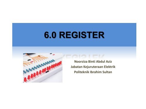
6.0 REGISTER<br />
Noorziza Binti Abdul Aziz<br />
Jabatan Kejuruteraan Elektrik<br />
Politeknik Ibrahim Sultan
Introduction<br />
• Shift registers are a type of sequential logic circuit,<br />
mainly for storage of digital data. They are a group of<br />
flip-flops connected in a chain so that the output from<br />
one flip-flop becomes the input of the next flip-flop.<br />
• Most of the registers possess no characteristic internal<br />
sequence of states.<br />
• Registers are synchronous circuits thus all flip-flops are<br />
controlled by a common clock line and all are set or<br />
reset simultaneously.<br />
• As registers are often use to collect serial data they are<br />
also called accumulators.
6.0 Register<br />
Register:<br />
• A set of n flip-flops<br />
• Each flip-flop stores one bit<br />
• An n-bit register has a group of n flip-flops.<br />
• Two basic functions: data storage and data movement.<br />
Shift Register:<br />
• A register that allows each of the flip-flops to pass the stored<br />
information to its adjacent neighbour<br />
Counter:<br />
• A register that goes through a predetermined sequence of<br />
states
• The usage of shift register can be seen<br />
in calculator functions.<br />
For example, try to press the key 1, then<br />
a number 1 will be displayed. When<br />
the second number is pressed, key<br />
8, then number 1 will be shifted to the<br />
left and number 18 will be displayed.<br />
• From the<br />
example above, we find that there have<br />
a logic circuit that was stored in<br />
calculator and will store<br />
the first number (for<br />
temporary) and then the<br />
number will shifted if the second<br />
number was entered.
D flip flop as a memory devices<br />
As a flip-flop can store only one<br />
bit of data, the device registers<br />
or memory capacity is equal<br />
to the number of flipflops<br />
are used. This means<br />
that if we want to build a 2-bit<br />
shift register, the two flip-flops<br />
are needed.<br />
2 Bits Shift Register
Types of shift register<br />
• the basic types of shift registers<br />
(i) Serial In - Serial Out (SISO)<br />
(ii) Serial In - Parallel Out (SIPO)<br />
(iii) Parallel In – Serial Out (PISO)<br />
(i) Parallel In - Parallel Out (PIPO)
Functions of shift register<br />
i. Storing data<br />
ii. Moving data<br />
iii. Convert serial data to parallel data.<br />
iv. Convert parallel data to serial data .<br />
v. Arithmetic logic in division and<br />
multiplying
Serial In - Serial Out<br />
• Block diagram:<br />
The diagram shows four flip-flops connected to form a<br />
SERIAL IN, SERIAL OUT shift register.
• Upon the arrival of a clock pulse,<br />
data at the D input of each flip-flop<br />
is transferred to its Q output.<br />
1<br />
CLK<br />
1<br />
• At the start, the contents of the<br />
register can be set to zero by means<br />
of the CLEAR line.<br />
• If a 1 is applied to the input of the<br />
first flip-flop, then upon the arrival<br />
of the first clock pulse, this 1 is<br />
transferred to the output of flip-flop<br />
1 (input of flip-flop 2).<br />
• After four clock pulses this 1 will be<br />
at the output of flip-flop 4.<br />
1<br />
1<br />
CLK<br />
2<br />
CLK<br />
3<br />
• In this manner, a four bit number<br />
can be stored in the register.<br />
• After four more clock pulses, this<br />
data will be shifted out of the<br />
register.<br />
1<br />
CLK<br />
4
Data movement using<br />
SISO shift register
Serial In - Parallel Out<br />
• Data is fed into the SERIAL IN/PARALLEL OUT shift<br />
register bit by bit, in the same way as for the SISO shift<br />
register.<br />
• However the four bits are all shifted out simultaneously,<br />
in parallel, as one word.
Serial In<br />
10010110
Parallel In – Serial Out<br />
• With the PARALLEL IN/SERIAL OUT shift<br />
register, four bits are shifted into the register<br />
simultaneously, in parallel.<br />
• They are then clocked out, one after the other,<br />
in serial form.
Parallel In<br />
Serial Out
Parallel In - Parallel Out<br />
• The PARALLEL IN/PARALLEL OUT shift register is loaded with four<br />
bits simultaneously, in parallel.<br />
• They are also clocked out simultaneously, in parallel.
Parallel In<br />
Example of data moving<br />
Parallel Out
(i)<br />
Shift register as divider circuits<br />
(Right Shift Register)<br />
• The number shifted from MSB (most significant bit) to LSB<br />
(least significant bit) which shifted from left to right.<br />
• Bit ‘0’ is inserted to MSB<br />
• Example:<br />
Binary<br />
Decimal<br />
Original number 01011000 88<br />
Shift#1 00101100 44<br />
Shift#2 00010110 22
Right shift register circuit<br />
Serial input<br />
D<br />
clk<br />
QA<br />
QA<br />
D<br />
clk<br />
QB<br />
QB<br />
D<br />
clk<br />
QC<br />
QC<br />
D QD<br />
clk<br />
QD<br />
Serial Output<br />
CLK
(ii)<br />
Shift register as multiplier circuits<br />
(Left Shift Register)<br />
• The number is shifted from LSB to MSB (shifted<br />
from right)<br />
• Bit ‘0’ is inserted to LSB.<br />
Binary<br />
Decimal<br />
Original number 00010110 22<br />
Shift#1 00101100 44<br />
Shift#2 01011000 88
Left shift register circuit<br />
Serial Output<br />
Serial Input<br />
D<br />
clk<br />
QA<br />
QA<br />
D<br />
clk<br />
QB<br />
QB<br />
D<br />
clk<br />
QC<br />
QC<br />
D QD<br />
clk<br />
QD<br />
CLK
Shift Register Counters<br />
• They are basically shift registers with the serial<br />
outputs connected back to the serial inputs in<br />
order to produce particular sequences.<br />
• These registers are classified as counters<br />
because they exhibit a specified sequence of<br />
states.
(i) Ring Counter<br />
• A ring counter is basically a circulating shift<br />
register in which the output of the most<br />
significant stage is fed back to the input of the<br />
least significant stage.<br />
• The following is a 4-bit ring counter constructed<br />
from D flip-flops.<br />
• The output of each stage is shifted into the next<br />
stage on the positive edge of a clock pulse.<br />
• If the CLEAR signal is high, all the flipflops except<br />
the first one FF0 are reset to 0. FF0 is preset to 1<br />
instead.
4 bit Ring Counter
Data movement in<br />
Ring Counter 4 bit
(i) Johnson Counter<br />
• Johnson counters are a variation of<br />
standard ring counters, with the inverted<br />
output of the last stage fed back to the<br />
input of the first stage.<br />
• They are also known as twisted ring<br />
counters. An n-stage Johnson counter<br />
yields a count sequence of length 2n, so it<br />
may be considered to be a mod-2n<br />
counter.
6 bit Johnson Counter
4 bit Johnson Counter<br />
data movement