TN1213 - LatticeXP2 Slave SPI Port User's Guide
TN1213 - LatticeXP2 Slave SPI Port User's Guide
TN1213 - LatticeXP2 Slave SPI Port User's Guide

You also want an ePaper? Increase the reach of your titles
YUMPU automatically turns print PDFs into web optimized ePapers that Google loves.
June 2012 Technical Note <strong>TN1213</strong><br />
Introduction<br />
The Serial Peripheral Interface (<strong>SPI</strong>) is the industry standard interface that can be found on most CPU and serial<br />
Flash memory devices. The drivers for reading and writing from memory devices are readily available on modern<br />
digital systems.<br />
This application note describes the programming detail using the built-in <strong>SPI</strong> port in the <strong>LatticeXP2</strong> devices to program<br />
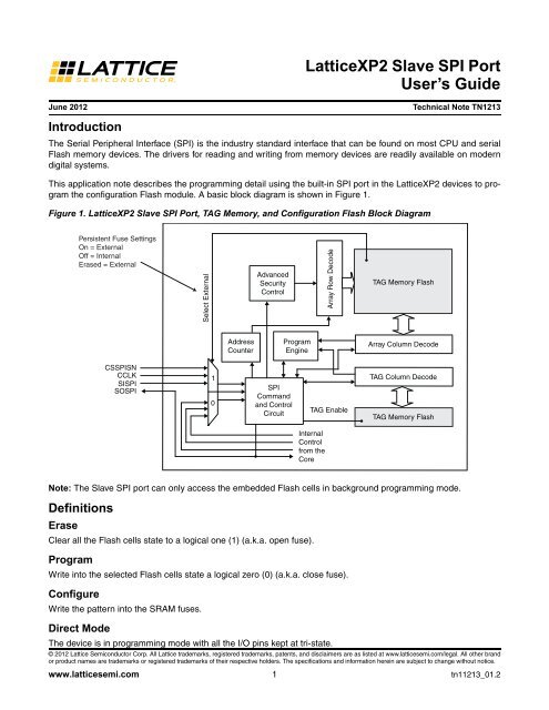
the configuration Flash module. A basic block diagram is shown in Figure 1.<br />
Figure 1. <strong>LatticeXP2</strong> <strong>Slave</strong> <strong>SPI</strong> <strong>Port</strong>, TAG Memory, and Configuration Flash Block Diagram<br />
Note: The <strong>Slave</strong> <strong>SPI</strong> port can only access the embedded Flash cells in background programming mode.<br />
Definitions<br />
Erase<br />
Clear all the Flash cells state to a logical one (1) (a.k.a. open fuse).<br />
Program<br />
Write into the selected Flash cells state a logical zero (0) (a.k.a. close fuse).<br />
Configure<br />
Persistent Fuse Settings<br />
On = External<br />
Off = Internal<br />
Erased = External<br />
Write the pattern into the SRAM fuses.<br />
Direct Mode<br />
CS<strong>SPI</strong>SN<br />
CCLK<br />
SI<strong>SPI</strong><br />
SO<strong>SPI</strong><br />
Address<br />
Counter<br />
<strong>SPI</strong><br />
Command<br />
and Control<br />
Circuit<br />
Program<br />
Engine<br />
The device is in programming mode with all the I/O pins kept at tri-state.<br />
Select External<br />
1<br />
0<br />
Advanced<br />
Security<br />
Control<br />
<strong>LatticeXP2</strong> <strong>Slave</strong> <strong>SPI</strong> <strong>Port</strong><br />
User’s <strong>Guide</strong><br />
Internal<br />
Control<br />
from the<br />
Core<br />
TAG Memory Flash<br />
Array Column Decode<br />
TAG Column Decode<br />
TAG Memory Flash<br />
© 2012 Lattice Semiconductor Corp. All Lattice trademarks, registered trademarks, patents, and disclaimers are as listed at www.latticesemi.com/legal. All other brand<br />
or product names are trademarks or registered trademarks of their respective holders. The specifications and information herein are subject to change without notice.<br />
www.latticesemi.com 1 tn11213_01.2<br />
Array Row Decode<br />
TAG Enable
Background Mode<br />
The device is in programming mode with all the I/O pins remain operational.<br />
Built-In Feature<br />
A feature comes with the silicon without pre-instantiation.<br />
Dedicated Pin<br />
The pin has only one function.<br />
Dual Purpose Pin<br />
The pin has more than one function.<br />
Secure<br />
Protect the Flash and SRAM fuses from reading.<br />
Advanced Security<br />
2<br />
<strong>LatticeXP2</strong> <strong>Slave</strong> <strong>SPI</strong> <strong>Port</strong> User’s <strong>Guide</strong><br />
The advanced features that provide additional security to the device, for example, Encryption, Flash Protect, or<br />
One Time Programmable (OTP) features.<br />
Master <strong>SPI</strong><br />
Industry standard Serial Peripheral Interface (<strong>SPI</strong>) used to configure the SRAM fuses from the bitstream stored in<br />
an external <strong>SPI</strong> Flash device.<br />
<strong>Slave</strong> <strong>SPI</strong> (S<strong>SPI</strong>)<br />
Access the <strong>SPI</strong> port through the Dual Purpose I/O pins.<br />
Internal <strong>SPI</strong><br />
Access the <strong>SPI</strong> port through the FPGA fabric.<br />
Refresh<br />
Initiates the device to reconfigure the SRAM fuses from the embedded configuration Flash fuses or external <strong>SPI</strong><br />
Flash device, depending on the configuration mode selected.<br />
Self Download Mode (SDM)<br />
Upon power up or a Refresh, the device is configured by a massive parallel transfer of the data programmed in the<br />
embedded configuration Flash fuses to the SRAM fuses.<br />
JEDEC File (.JED File)<br />
The programming data file as defined by JEDEC 42.1C standard. The programming file is expressed in the ASCII 1<br />
and 0 format. The file is printable. 3 rd party programmers use it to support large volume production programming.<br />
Binary Data File (.BIN File)<br />
The programming data file converted from the JEDEC file. The programming file is expressed in binary hex format.<br />
The file is not printable.<br />
The conversion utility, in C source code form or compiled program form, is available from Lattice.<br />
Bitstream Data File (.BIT File)<br />
The configuration data file in the format that can be loaded directly into the FPGA devices to configure the SRAM<br />
cells. The file is expressed in binary hex format. The file is not printable.
Dual Boot<br />
3<br />
<strong>LatticeXP2</strong> <strong>Slave</strong> <strong>SPI</strong> <strong>Port</strong> User’s <strong>Guide</strong><br />
The device can boot from two sources: the embedded Flash in the device or an external <strong>SPI</strong> Flash. Depending on<br />
configuration, the device may use one as primary source and the other as golden source. (Note: The only way to<br />
select this feature is by holding the CFG0 pin statically to low before, during and after powering up the <strong>LatticeXP2</strong><br />
device.)<br />
Row<br />
A row is one address location selected by the address pointer inside the <strong>LatticeXP2</strong> device.<br />
Column<br />
A column is one data bit location in the row (or address) currently selected by the address pointier.<br />
Hardware Interfaces<br />
The following is a list of built-in interfaces that are available on the <strong>LatticeXP2</strong> family.<br />
• <strong>Slave</strong> <strong>SPI</strong><br />
– Dedicated and always available except when:<br />
- The device is set into JTAG programming mode by the JTAG port.<br />
- The Master <strong>SPI</strong> interface is active.<br />
– Supports the industry standard <strong>SPI</strong> protocol.<br />
- OPCODE = 8 bits.<br />
- Command = 32 bits (8-bit OPCODE + 24-bit operand).<br />
- Supports intelligent Flash programming.<br />
- Programming action triggered by a low to high edge on the CSN pin.<br />
– External/Internal <strong>Slave</strong> <strong>SPI</strong> interface.<br />
- The external <strong>SPI</strong> interface is automatically selected when the device is erased.<br />
- Persistent Fuse Settings:<br />
On: Selects the External Interface (SI<strong>SPI</strong>, SO<strong>SPI</strong>, CS<strong>SPI</strong>SN, and CCLK).<br />
Off: Selects the Internal Interface (four CIB signals of the S<strong>SPI</strong>A core).<br />
– Supports JEDEC files.<br />
- Standard<br />
- Encrypted<br />
Master <strong>SPI</strong> (Power up with CFG0 = 0)<br />
– Supports industry standard <strong>SPI</strong> Flash devices.<br />
– Supports standard FPGA bitstream file (Encrypted bit-streams are not supported).<br />
ispJTAG (1149.1 Interface)<br />
– IEEE 1149.1 and IEEE 1532 compliant.<br />
– Dedicated and always available.<br />
General Descriptions<br />
If the CFG0 pin is tied to VCC, the <strong>LatticeXP2</strong> device is in Self Download Mode (SDM). In this mode, the<br />
<strong>LatticeXP2</strong> family of devices is designed with two standard programming ports, JTAG and <strong>Slave</strong> <strong>SPI</strong>. A basic block<br />
diagram is shown in Figure 2.
Figure 2. Self Download Mode with Persistent Enabled<br />
VCC<br />
CFG0<br />
SO<strong>SPI</strong><br />
SI<strong>SPI</strong><br />
CCLK<br />
CS<strong>SPI</strong>SN<br />
ispJTAG (1149.1 Interface)<br />
4<br />
<strong>LatticeXP2</strong> <strong>Slave</strong> <strong>SPI</strong> <strong>Port</strong> User’s <strong>Guide</strong><br />
The JTAG port is the primary programming port. The JTAG pins are hardwired as required by the IEEE 1532 standard.<br />
The four JTAG pins can never be recovered as user I/O pins. As the primary programming port, all programming<br />
activities can be carried out on this port. Particularly, the Advanced Security features, such as enabling the<br />
Flash Protect, enabling the encryption, and programming the password and keys into the device can only be done<br />
on this port.<br />
<strong>Slave</strong> <strong>SPI</strong><br />
The <strong>Slave</strong> <strong>SPI</strong> port is the secondary programming port. The four <strong>SPI</strong> pins are dual-purpose pins, not dedicated. All<br />
four <strong>SPI</strong> pins can be recovered as user I/O pins when the Persistent option is disabled. The Persistent option will<br />
be disabled by the software unless the user sets the SLAVE_<strong>SPI</strong>_PORT to Enable using the Design Planner in isp-<br />
LEVER ® . This option is shown in the Global tab of the Design Planner Spreadsheet view. As a secondary port, only<br />
a subset of the programming activities is available from this port.<br />
Program and verify an encrypted or standard JEDEC file into embedded configuration Flash in background mode<br />
only. Direct programming mode is not supported.<br />
Read the SRAM fuse cells in background mode only. The SRAM fuse configuration is not supported.<br />
Trigger a Refresh operation to download the embedded configuration Flash to the SRAM cells. The TransFR feature<br />
is not available on <strong>SPI</strong> port. The I/O pins will all be tri-stated during the Refresh.<br />
The <strong>LatticeXP2</strong> devices are shipped from Lattice with an erased embedded configuration Flash. The persistent<br />
fuse is On in the erased state, which is equivalent to setting the SLAVE_<strong>SPI</strong>_PORT to Enable in ispLEVER. Therefore,<br />
the <strong>Slave</strong> <strong>SPI</strong> interface is enabled when the <strong>LatticeXP2</strong> devices are shipped from Lattice. It is up to the user<br />
to select the desired setting in ispLEVER before generating the JEDEC file.<br />
This application note assumes that the SLAVE_<strong>SPI</strong>_PORT is set to Enable in ispLEVER when the JEDEC file is<br />
generated.<br />
This application note also assumes that the Flash Protect password and the encryption key are already programmed<br />
into the device. The Flash Protect password and the encryption key can only be programmed into the<br />
device using the JTAG port.<br />
Pin Descriptions<br />
Serial Data Input (SI<strong>SPI</strong>)<br />
The <strong>SPI</strong> Serial Data Input pin is for commands and data to be serially written to (shifted into) the device. Data is<br />
latched on the rising edge of serial clock (CCLK) input pin.<br />
Serial Data Output (SO<strong>SPI</strong>)<br />
<strong>LatticeXP2</strong><br />
TDO<br />
TDI<br />
TCK<br />
TMS<br />
Legend: Solid Lines = Dedicated JTAG Pins<br />
Dashed Lines = Dual Purpose S<strong>SPI</strong> Pins<br />
The <strong>SPI</strong> Serial Data Output pin is for status and data to be serially read out (shifted out of) the device. Data is<br />
shifted out on the falling edge of serial clock (CCLK) input pin.
Serial Clock (CCLK)<br />
The <strong>SPI</strong> Serial Clock Input pin provides the timing for serial input and output operations.<br />
Chip Select (CS<strong>SPI</strong>SN)<br />
5<br />
<strong>LatticeXP2</strong> <strong>Slave</strong> <strong>SPI</strong> <strong>Port</strong> User’s <strong>Guide</strong><br />
The <strong>SPI</strong> Chip Select pin enables and disables (reset) <strong>SPI</strong> interface operations. When the Chip Select transits from<br />
low to high the <strong>SPI</strong> interface is reset into a ready for command state and the Serial Data Output (SO<strong>SPI</strong>) pin is at<br />
high impedance. When it is brought from high to low, the <strong>SPI</strong> interface is selected, commands can be written into<br />
and data read from the device. After power up, this pin must transit from high to low before a new command can be<br />
accepted.<br />
<strong>SPI</strong> Operations<br />
<strong>SPI</strong> Modes<br />
The <strong>SPI</strong> interface is accessible through the <strong>SPI</strong> compatible bus consisting of four signals: Serial Clock (CCLK),<br />
Chip Select (CS<strong>SPI</strong>SN), Serial Data Input (SI<strong>SPI</strong>), and Serial Data Output (SO<strong>SPI</strong>). Both <strong>SPI</strong> bus operation Modes<br />
0 (0,0) and 3 (1,1) are supported. The primary difference between Mode 0 and Mode 3 concerns the normal state<br />
of the CCLK pin when the <strong>SPI</strong> master is in standby and data is not being transferred to the device’s <strong>SPI</strong> interface.<br />
For Mode 0, CCLK is normally low. For Mode 3, the CCLK signal is normally high. In either case, data input on the<br />
SI<strong>SPI</strong> pin is sampled only during the rising edge. Data output on the SO<strong>SPI</strong> pin is clocked out only on the falling<br />
edge of CCLK.<br />
Device Status Register<br />
The <strong>LatticeXP2</strong> has an 8-bit device status register, which indicates the status of the device, as defined in Table 1.<br />
Table 1. 8-Bit Device Status Register<br />
Bit State<br />
Status Bit Description<br />
0 1<br />
B0 The status of the erase operation just completed (see Note 1). Pass Fail<br />
B1 The state of the Done fuse. Erase Programmed<br />
B2 The test result of the Flash Protect Key entered. Match No Match<br />
B3 Reserved (see Note 2). Default<br />
B4 The OTP (One Time Programmable) fuse setting. Off On<br />
B5 The Flash Protect setting. Disabled Enabled<br />
B6 The Encryption setting. Disabled Enabled<br />
B7 The standard security fuse setting. Erase Programmed<br />
Notes:<br />
1. This covers the ERASE and ERASE_TAG command. The one bit status bit accessed by the PROGRAM_STATUS command only indicates if<br />
the erase action has completed. However, it does not indicate if it passed or failed. Thus, this bit is defined to indicate whether the erase<br />
operation passed or failed. A Pass means all the cells were erased with the proper margin per the data retention requirement. A Fail means<br />
some cells fail to be erased to the proper margin.<br />
2. If the SED (Soft Error Detection) feature is selected, this bit shows the comparison result of the SED CRC. If the SED feature is selected, the<br />
SED must not be running when using the <strong>SPI</strong> port to program the device. The SED engine and programming engine use the same data shift<br />
register. Only one task can use the data shift register at one time. Otherwise, the result will be unpredictable.<br />
Program Status Register<br />
The <strong>LatticeXP2</strong> has a 1-bit program status register, which indicates when the erase or program action is completed,<br />
as defined in Table 2.
Table 2. 1-Bit Program Status Register<br />
Program Status<br />
Register Value Status<br />
0 Not Complete<br />
1 Completed<br />
<strong>Slave</strong> <strong>SPI</strong> Programming Flow Diagrams<br />
6<br />
<strong>LatticeXP2</strong> <strong>Slave</strong> <strong>SPI</strong> <strong>Port</strong> User’s <strong>Guide</strong><br />
The <strong>LatticeXP2</strong> can be programmed with a standard or encrypted JEDEC file, as shown in Figure 3.<br />
Note: The JEDEC files must first be converted from an ASCII binary format to a binary HEX format using the<br />
JED2HEX utility or ispVM ® System Software.<br />
Figure 3. <strong>Slave</strong> <strong>SPI</strong> Programming Flow for Standard and Encrypted JEDEC Files<br />
On<br />
Blank<br />
Device<br />
Program TAG and<br />
Configuration Flash<br />
by External <strong>SPI</strong><br />
Interface<br />
Programmed<br />
Device<br />
Persistent Fuse<br />
= ?<br />
Off<br />
Program TAG and<br />
Configuration Flash<br />
by Internal <strong>SPI</strong><br />
Interface<br />
Standard<br />
JEDEC<br />
Encryption<br />
Enabled<br />
Device<br />
Program TAG and<br />
Configuration Flash<br />
by External <strong>SPI</strong><br />
Interface<br />
Programmed<br />
Device<br />
Persistent Fuse<br />
= ?<br />
Program TAG and<br />
Configuration Flash<br />
by Internal <strong>SPI</strong><br />
Interface<br />
Encrypted<br />
JEDEC<br />
The <strong>LatticeXP2</strong> <strong>Slave</strong> <strong>SPI</strong> programming algorithm for the embedded configuration Flash resembles the popular<br />
standard <strong>SPI</strong> Flash memory devices available in the market place. The erase, program, and verify flow diagrams<br />
are shown in Figure 4 through Figure 10.<br />
Note: Please refer to Table 6 for the erase and program loop delays and maximun number of loops. Please refer to<br />
Table 8 for the number of rows and columns for each member of the <strong>LatticeXP2</strong> family.<br />
On<br />
Off
Figure 4. Check ID and Erase Flow Diagram<br />
Optional Block.<br />
Skip if No Flash Protect<br />
No<br />
Loop=Max?<br />
STOP<br />
11<br />
Yes<br />
3<br />
1<br />
7<br />
<strong>LatticeXP2</strong> <strong>Slave</strong> <strong>SPI</strong> <strong>Port</strong> User’s <strong>Guide</strong><br />
Start<br />
Clock In Read_ID Command<br />
Clock Out 32-bit JTAG IDCODE and Compare<br />
Match?<br />
Set Device into Background Programming Mode<br />
9<br />
7<br />
8<br />
5<br />
12<br />
No<br />
Flash Protect<br />
Enabled (B5)?<br />
Load Password<br />
Clock in 64-bit Password<br />
Check Status<br />
Register B2<br />
DISABLE_DONE Command<br />
Clock in Erase Command<br />
Pause for Erase Pulse Delay<br />
No<br />
Erase Status<br />
Completed?<br />
Yes<br />
6<br />
Fail<br />
Check Status<br />
Register B0<br />
Pass<br />
Initialize Address<br />
1<br />
2<br />
4<br />
6<br />
Pass<br />
10<br />
Pass<br />
Yes<br />
Fail<br />
Fail<br />
STOP
Figure 5. Standard and Encrypted Programming Flow Diagram<br />
No<br />
14<br />
11<br />
Standard JEDEC Programming Flow<br />
Program Increment<br />
Program Status<br />
Complete?<br />
1<br />
8<br />
<strong>LatticeXP2</strong> <strong>Slave</strong> <strong>SPI</strong> <strong>Port</strong> User’s <strong>Guide</strong><br />
Encrypted JEDEC Programming Flow<br />
Reset Data CRC<br />
Clock In One Row of Programming Date 17 Encrypt Program Increment<br />
9<br />
Yes<br />
13<br />
Not Set<br />
Loop = Max?<br />
STOP<br />
Pause for Program Pulse Delay 18 Clock In One Frame of Encrypted Programming Data<br />
Fail<br />
Row = Max?<br />
1-0<br />
Set<br />
Check Status<br />
Register B0<br />
Pass<br />
Yes<br />
10<br />
6<br />
15<br />
No<br />
No<br />
16<br />
9<br />
Not Set<br />
Loop = Max?<br />
Yes<br />
STOP<br />
Pause for Program Pulse Delay<br />
Fail<br />
Program Status<br />
Completed?<br />
Check Status<br />
Register B0<br />
Pass<br />
Loop=Max?<br />
1-1<br />
Set<br />
Yes<br />
10<br />
6<br />
15<br />
No
Figure 6. Program SED CRC and Verify Flow Diagram<br />
Program SED CRC<br />
Program Status<br />
Complete?<br />
9<br />
<strong>LatticeXP2</strong> <strong>Slave</strong> <strong>SPI</strong> <strong>Port</strong> User’s <strong>Guide</strong><br />
Standard Flow Encryption Flow<br />
1-0<br />
1-1<br />
No<br />
9<br />
STOP<br />
19<br />
Not Set<br />
Loop = Max?<br />
Yes<br />
STOP<br />
Optional Block.<br />
Skip if No SED CRC.<br />
Program SED CRC<br />
Clock In 32-bit SED CRC Data Clock In 32-bit SEC CRC Data<br />
Pause for Program Pulse Delay<br />
No<br />
Row = Max?<br />
2<br />
Set<br />
10<br />
Read SED CRC<br />
Clock Out the<br />
32-bit SEC CRC<br />
and Compare<br />
Match?<br />
Yes<br />
Initialize Address<br />
Verify Increment<br />
Yes<br />
2<br />
15<br />
22<br />
23<br />
12<br />
20<br />
Clock Out One for Row of Data and Compare<br />
Match?<br />
Yes<br />
2<br />
No<br />
No<br />
STOP<br />
21<br />
9<br />
19<br />
Pause for Program Pause Delay<br />
38<br />
Program Status<br />
Completed?<br />
Set<br />
Read Data CRC<br />
Clock Out the 16-bit Data CRC and Compare<br />
Match?<br />
2<br />
Yes<br />
10<br />
Not Set<br />
Loop = Max?<br />
STOP<br />
No<br />
39<br />
STOP
Figure 7. Program and Verify USERCODE Flow Diagram<br />
24<br />
25<br />
9<br />
26<br />
2<br />
Program USERCODE<br />
Clock In 32-bit USERCODE Data<br />
Pause for Program Pulse Delay<br />
Program Status<br />
Completed?<br />
Set<br />
Read USERCODE<br />
Clock Out 32-bit USERCODE Data and Compare<br />
Match?<br />
3<br />
Yes<br />
10<br />
2<br />
10<br />
Not Set<br />
No<br />
<strong>LatticeXP2</strong> <strong>Slave</strong> <strong>SPI</strong> <strong>Port</strong> User’s <strong>Guide</strong><br />
Optional Block.<br />
Skip if No USERCODE.<br />
Loop = Max?<br />
Yes<br />
STOP<br />
11<br />
No
Figure 8. Program Security and Done Fuse Flow Diagram<br />
11<br />
<strong>LatticeXP2</strong> <strong>Slave</strong> <strong>SPI</strong> <strong>Port</strong> User’s <strong>Guide</strong><br />
Standard Flow Encryption<br />
27<br />
Program<br />
Security?<br />
Program Security<br />
Pause for Program Pulse Delay<br />
Program Status<br />
Complete?<br />
Set<br />
6<br />
Check Status<br />
Register B7<br />
Pass<br />
Yes<br />
10<br />
No<br />
28<br />
Not Set<br />
Loop = Max?<br />
Fail<br />
9<br />
STOP<br />
29<br />
9<br />
11<br />
Yes<br />
No<br />
3<br />
Program Done Fuse<br />
Pause for Program Pulse Delay<br />
6<br />
4<br />
Pass<br />
10<br />
Program Status<br />
Complete?<br />
Set<br />
Check Status<br />
Register B0<br />
Fail<br />
Program Security<br />
Pause for Program Pulse Delay<br />
Not Set<br />
Program Status<br />
Completed?<br />
6<br />
Yes<br />
Check Status<br />
Register B7<br />
11<br />
Loop = Max?<br />
STOP<br />
Pass<br />
No<br />
10<br />
28<br />
9<br />
Loop = Max?<br />
Fail<br />
STOP<br />
11<br />
Yes<br />
No
Figure 9. Program TAG Flow Diagram<br />
36<br />
35<br />
33<br />
9<br />
31<br />
9<br />
32<br />
4<br />
Program TAG<br />
Erase TAG<br />
Pause for Erase Pulse Delay<br />
10<br />
Program Status<br />
Completed?<br />
Program TAG<br />
Clock In One Page of TAG Memory Data<br />
34<br />
No<br />
Pause for Program Pulse Delay<br />
Program Status<br />
Completed?<br />
Read TAG<br />
Clock Out One Page of TAG Memory Data<br />
Match?<br />
Terminate the Background Programming Mode<br />
5<br />
Yes<br />
Set<br />
Set<br />
Yes<br />
2<br />
12<br />
10<br />
30<br />
<strong>LatticeXP2</strong> <strong>Slave</strong> <strong>SPI</strong> <strong>Port</strong> User’s <strong>Guide</strong><br />
No<br />
Not Set<br />
Not Set<br />
Loop = Max?<br />
STOP<br />
STOP<br />
11<br />
Yes<br />
11<br />
Loop = Max?<br />
Yes<br />
No<br />
No
Figure 10. Refresh Flow Diagram<br />
37<br />
42<br />
No<br />
Load Refresh Command<br />
Pause for Refresh Delay<br />
6<br />
5<br />
Refresh?<br />
Yes<br />
Check Status<br />
Register B1<br />
Finish<br />
13<br />
Pass<br />
<strong>LatticeXP2</strong> <strong>Slave</strong> <strong>SPI</strong> <strong>Port</strong> User’s <strong>Guide</strong><br />
37<br />
Fail<br />
Done = 1<br />
STOP<br />
Done = 0
Commands Table<br />
Table 3. <strong>Slave</strong> <strong>SPI</strong> Command Table<br />
Command Name Byte 0 Bytes 1-3 Description<br />
READ_ID 0x98 Dummy Read 32-bit JTAG IDCODE.<br />
X_PROGRAM_EN 0xAC Dummy<br />
X_SRAM_READ_EN 0xAE Dummy<br />
14<br />
<strong>LatticeXP2</strong> <strong>Slave</strong> <strong>SPI</strong> <strong>Port</strong> User’s <strong>Guide</strong><br />
Enable Background Flash Mode to activate the Flash erase, programming,<br />
and read back command.<br />
Enable Background SRAM Mode to activate the read (VERIFY_INC)<br />
command to target at the SRAM fuses instead of the Flash fuses.<br />
READ_TAG 0x4E Dummy<br />
Read TAG Memory. Use the command sequence as shown to read TAG<br />
memory. X_PROGRAM_EN, READ_TAG, PROGRAM_DIS. The<br />
sequence is necessary to minimize the stress to the Flash cells or to<br />
maximize the read cycle endurance.<br />
PROGRAM_TAG 0x8E Dummy Program TAG Memory.<br />
ERASE_TAG 0x0E Dummy Erase TAG Memory.<br />
READ_PROGRAM_STATUS 0x4A Dummy<br />
Read out the one bit programming status register. 1 = erase or programming<br />
action complete. 0 = action not yet started or already in progress.<br />
PROGRAM_DIS 0x78 Dummy Terminate the effect of the previously loaded enable command.<br />
DISABLE_DONE 0x24 Dummy Erase the bit indicating the internal Flash has a valid pattern.<br />
ERASE 0xC0 Dummy Erase Configuration Flash.<br />
READ_USERCODE 0xE8 Dummy Read 32-bit Flash or SRAM USERCODE.<br />
PROGRAM_USERCODE 0x58 Dummy Program 32-bit USERCODE.<br />
INIT_ADDRESS 0x84 Dummy Sets the Configuration Flash address to the first row.<br />
PROGRAM_INC 0xE6 Dummy<br />
Programs one row of configuration Flash, then increments the row<br />
address.<br />
VERIFY_INC 0x56 Dummy<br />
Reads one row of configuration Flash or SRAM fuses, then increment<br />
the row address.<br />
Note: This command will not work if the encryption feature already<br />
enabled.<br />
PROGRAM_SED_CRC 0xA2 Dummy Program the 32-bit SED CRC fuses.<br />
READ_SED_CRC 0x22 Dummy Read the 32-bit SED CRC fuses.<br />
PROGRAM_SECURITY 0x90 Dummy Program Security Fuse<br />
PROGRAM_DONE 0xF4 Dummy Program the DONE fuse.<br />
REFRESH 0xC4 Dummy<br />
ENCRYPT_PROGRAM_INC 0x02 Dummy<br />
Tri-state I/O and clear all SRAM fuses. If the done fuse is programmed,<br />
trigger a Configuration Flash to SRAM transfer. If the done fuse is not<br />
programmed, the Flash to SRAM transfer will not happen.<br />
Note: This command will not work if PROGRAM_DIS is not issued.<br />
Please refer to the flow.<br />
Program one row of encrypted data into the configuration Flash then<br />
increment the row address.<br />
Note: The command works only if the encryption feature already<br />
enabled.<br />
PROTECT_SHIFT 0x82 Dummy<br />
Program the 64-bit Flash Protect Password to unlock Configuration<br />
Flash for reprogramming.<br />
READ_DEVICE_STATUS 0x4D Dummy Read the 8-bit device status register.<br />
READ_16_CRC 0xA3 Dummy Read the 16-bit CRC value from the CRC engine.<br />
RESET_16_CRC 0x63 Dummy Initialize the 16-bit CRC engine to 0.<br />
Notes:<br />
1. Commands are classified into classes for the convenience of waveform illustration.<br />
2. Byte 1-3 are dummy clocks to provide extra timing for the device to execute the command. The data presented at the SI pin during these<br />
dummy clocks can be any value and do not have to be 0x00 as shown.<br />
3. The READ_ID command reads out the 32-bit JTAG IDCODE of the device. The first bit shifted out on SO<strong>SPI</strong> pin is thus bit 0, which has the<br />
value = 1 as per IEEE 1149.1 standard of the JTAG IDCODE and the last bit is bit 31, which is the last bit of the revision field, of the IDCODE.
15<br />
<strong>LatticeXP2</strong> <strong>Slave</strong> <strong>SPI</strong> <strong>Port</strong> User’s <strong>Guide</strong><br />
4. The PROGRAM_STATUS command read from the single bit status register. When read from the register, only the 1 st bit is valid, the other<br />
bits are dummies and should be ignored.<br />
5. Shift into the device an invalid OPCODE will cause the 1 bit bypass register connected to the SO<strong>SPI</strong> pin.<br />
6. If there is under clocking, the CS<strong>SPI</strong>SN pin is driven from low to high before enough clocks were applied, the device will behave as follows:<br />
a. If under clocking on the 8-bit IDOCDE, it has the same effect as an invalid OPCODE.<br />
b. If under clocking on the 24-bit dummy, the action of the command won’t take place.<br />
c. If under clocking on shifting out data, the remaining un-read data will be lost.<br />
d. If under clocking on shifting in programming data, the partial programming data will be programmed into the device.<br />
e. If there is over clocking, the CS<strong>SPI</strong>SN pin is driven from low to high after more than enough clocks were applied, the device will behave as<br />
follows:<br />
7. If over clocking on the 8-bit IDOCDE, the extra clocks will be treated as dummy.<br />
a. If over clocking on the 24-bit dummy, the extra clocks will be treated as data if it is a Class C or D command, otherwise they are ignored.<br />
b. If over clocking on shifting out data, the extra data being shifted out will be unknown.<br />
c. If over clocking on shifting in programming data, the extra clock will overflow the targeted data register.<br />
Use of Commands<br />
Table 4. <strong>Slave</strong> <strong>SPI</strong> Command Usage Table<br />
OPCODE<br />
Flow Operation<br />
Command Name MSB LSB Class Data Number Delay Time<br />
READ_ID 0x98 A Out 1, 2 None (see Note 1)<br />
X_PROGRAM_EN 0xAC E 3 None (see Note 1)<br />
X_SRAM_READ_EN 0xAE E See Note 3 None (see Note 1)<br />
READ_TAG 0x4E D Out 34, 35 5µs min. (see Note 1 and 2)<br />
PROGRAM_TAG 0x8E C In 32, 33, 34 See Table 6<br />
ERASE_TAG 0x0E B 31 SeeTable 7<br />
READ_PROGRAM_STATUS 0x4A D Out 9, 10, 11 = Delay of the previous command<br />
PROGRAM_DIS 0x78 E 36 1ms min.<br />
DISABLE_DONE 0x24 B 7 1ms min.<br />
ERASE 0xC0 B 8 See Table 7<br />
READ_USERCODE 0xE8 D Out 26 None (see Note 1)<br />
PROGRAM_USERCODE 0x58 C In 24, 25 1ms min., 25ms max.<br />
INIT_ADDRESS 0x84 E 12 None (see Note 1)<br />
PROGRAM_INC 0xE6 C In 13, 14 See Table 6<br />
VERIFY_INC 0x56 G Out 20, 21 5µs min.<br />
PROGRAM_SED_CRC 0xA2 C In 19 1ms min., 25ms max.<br />
READ_SED_CRC 0x22 D Out 22, 23 None (see Note 1)<br />
PROGRAM_SECURITY 0x90 B 27, 28 20ms min.<br />
PROGRAM_DONE 0xF4 B 29 1ms min., 25ms max.<br />
REFRESH 0xC4 E 37, 42 2ms min.<br />
ENCRYPT_PROGRAM_INC 0x02 C In 17, 18 1ms min., 25ms max.<br />
PROTECT_SHIFT 0x82 F In 5 None (see Note 1)<br />
READ_DEVICE_STATUS 0x4D D Out 4, 6 None (see Note 1)<br />
READ_16_CRC 0xA3 D Out 38, 39 None (see Note 1)<br />
RESET_16_CRC 0x63 E 16 None (see Note 1)<br />
Notes:<br />
1. The intrinsic delay provided by shifting in the twenty four (24) dummy bits, even if at 25 MHz, is sufficient and hence additional delay is not<br />
required.<br />
2. The READ_TAG command requires the X_PROGRAM_EN command is shifted into the device first to qualify the READ_TAG command.<br />
3. If this command, X_SRAM_READ_EN, is loaded instead of the X_PROGRAM_EN, the following commands will read out the SRAM fuses<br />
instead of from the Flash.<br />
VERIFY_INC
READ_SED_CRC<br />
READ_USERCODE<br />
This command has no effect on the READ_TAG command.<br />
Command Waveforms<br />
Class A Command Waveforms<br />
16<br />
<strong>LatticeXP2</strong> <strong>Slave</strong> <strong>SPI</strong> <strong>Port</strong> User’s <strong>Guide</strong><br />
The Class A commands is one that reads data out without an additional verification delay. The IDCODE command<br />
for reading out the 32-bit JTAG IDCODE is the only command in this class.<br />
Figure 11. Class A Command Waveforms<br />
CS<strong>SPI</strong>SN<br />
CCLK<br />
SI<strong>SPI</strong><br />
SO<strong>SPI</strong><br />
MSB<br />
Class B Commands Waveform<br />
The Class B commands require a delay to execute the action associated with the command. These types of commands<br />
can only initiate it’s own action. It cannot terminate the action of any commands, even it’s own action. The<br />
device requires three (3) extra clocks after the rising edge of CS<strong>SPI</strong>SN to initiate the action. After the specified<br />
delay time, the PROGRAM_STATUS command should be used to check if the action is completed. This will eliminate<br />
the possibility of having more than one action in progress at a giving time, which could cause the actions to<br />
clash.<br />
Figure 12. Class B Command Waveforms<br />
CS<strong>SPI</strong>SN<br />
CCLK<br />
SIPI<br />
SO<strong>SPI</strong><br />
OPCODE<br />
Tri-state<br />
8-Bit OPCODE<br />
LSB<br />
Class C Commands Waveforms<br />
SO<strong>SPI</strong> enabled by the falling edge<br />
of the 24 th dummy clock<br />
0 1 2 N-1<br />
24-Bit Dummy Valid Data<br />
3 Extra Clocks Required to Initiate Action<br />
OPCODE<br />
Tri-state<br />
8-Bit OPCODE<br />
Clocks are<br />
Optional while<br />
Pausing for<br />
Delay<br />
24-Bit Dummy Specified<br />
Delay Time<br />
SO<strong>SPI</strong> disabled by t<br />
rising edge of CSSP<br />
Tri-state<br />
The Class C commands are used for shifting data into the devices. All of the programming data registers are constructed<br />
as FIFO’s. The exact number of programming data bits must be provided to the selected programming<br />
data register. If over-shift or under-shift happens, the resulting data programmed into the device will be invalid.
17<br />
<strong>LatticeXP2</strong> <strong>Slave</strong> <strong>SPI</strong> <strong>Port</strong> User’s <strong>Guide</strong><br />
Operations in this class are PROGRAM_TAG, PROGRAM_USERCODE, PROGRAM_INC,<br />
PROGRAM_SED_CRC, and ENCRYPT_PROGRAM_INC.<br />
The actual configuration data may not be byte-bounded. Leading padding bits of zeros (0) can be used to pad the<br />
programming data into a byte bound hex file format. When shifting the programming data into the device, the overflowing<br />
characteristic of the FIFO behavior of the shift register is utilized to discard the leading padding bits. As a<br />
result, only the actual programming data will reside in the programming data register. The device requires three (3)<br />
extra clocks after the rising edge of CS<strong>SPI</strong>SN to initiate the action. After the specified delay time, the<br />
PROGRAM_STATUS command should be used to check if the action is completed. This will eliminate the possibility<br />
of having more than one action in progress at a giving time, which could cause the actions to clash.<br />
Figure 13. Type Programming Data Shift Register<br />
Figure 14. Class C Command Waveforms<br />
CS<strong>SPI</strong>SN<br />
CCLK<br />
SI<strong>SPI</strong><br />
SO<strong>SPI</strong><br />
Shifting in Data<br />
OPCODE<br />
Tri-state<br />
8-Bit OPCODE<br />
Class D Commands Waveforms<br />
Bit Size of this Register May Not be Divisible by 8<br />
Padding Bits when Applicable<br />
Discard Padding Bits by Overflowing<br />
3 Extra Clocks Required to Initiate Action<br />
Shift in the First Bit of Data<br />
0 1 2 N-1<br />
The Class D commands read data out from the device. The data can be device status, programming status, USER-<br />
CODE, or TAG Memory.<br />
When reading the TAG Memory data, there is a 5µs verify delay time required to provide the device the time it<br />
needs to physically transferring the data storing in Flash cells into the FIFO data shift register. The twenty four (24)<br />
clocks used to shift in the dummy bits are considered part of the delay by the device. If the twenty four (24) clocks<br />
are applied faster than 5µs, then extra delay is required by holding the CCLK low before sampling SO<strong>SPI</strong>.<br />
All commands in this class must be qualified by shifting in first the X_PROGRAM_EN command, which is equivalent<br />
to the WRITE_EN command in standard <strong>SPI</strong> Flash devices. If not, the transfer action will not happen, resulting<br />
in unknown data being shifted out.<br />
If the programming data size is not divisible by eight (8), trailing padding clocks can be used to shift out byte bound<br />
data and then discard the residual bits clocked out by the trailing padding clocks.<br />
0<br />
0<br />
0 0 0<br />
Clocks are<br />
Optional while<br />
Pausing for<br />
Delay<br />
24-Bit Dummy Programming Data<br />
Specified<br />
Delay Time<br />
Byte bound data shift into device<br />
Tri-state
18<br />
<strong>LatticeXP2</strong> <strong>Slave</strong> <strong>SPI</strong> <strong>Port</strong> User’s <strong>Guide</strong><br />
Note: Please refer to Table 8 for the number of data bits N (columns) for each member of the <strong>LatticeXP2</strong> family.<br />
Figure 15. Class D Command Waveforms<br />
CS<strong>SPI</strong>SN<br />
CCLK<br />
SI<strong>SPI</strong><br />
SO<strong>SPI</strong><br />
Data capture starts on the 21st dummy clock<br />
OPCODE<br />
Tri-state<br />
8-Bit OPCODE<br />
PROGRAM_STATUS (4Ah) Waveforms<br />
The PROGRAM_STATUS command is a Class D command. Instead of reading out programming data, a single bit<br />
programming status is read. This command determines if the erase action or programming action complete successfully.<br />
This command does not initiate, interrupt, or terminate the erase or programming action. It is used to interrogate<br />
the device to determine if the action initiated by the erase or programming command is done. If repetitive status bit<br />
polling is necessary, then repetitively issue the command and the twenty four (24) bits dummy.<br />
The actual bit size of the status bit register is one (1) bit. After the thirty two (32) clocks of command OPCODE and<br />
dummy, if eight (8) read clocks are applied for the convenience of the driver program, then only care about the first<br />
bit shifted out and ignore the rest.<br />
Figure 16. PROGRAM_STATUS Waveforms<br />
CS<strong>SPI</strong>SN<br />
CCLK<br />
Data capture starts on the 21st dummy clock<br />
Note 1<br />
SO<strong>SPI</strong> enabled by the falling<br />
edge of the 24th dummy clock<br />
0 1 2 N-1<br />
Tri-state<br />
24-Bit Dummy<br />
Valid Data<br />
The exact state of the padding bits<br />
shifted by over-clocking is unknown.<br />
They should be discarded.<br />
Provide device additional Erase of Program Time<br />
Next Command<br />
1 of 8 clocks to shift data<br />
SI<strong>SPI</strong> PROGRAM STATUS<br />
SO<strong>SPI</strong><br />
Tri-state<br />
SO<strong>SPI</strong> enabled by the falling<br />
edge of the 24th dummy clock<br />
0 1 2 6 7<br />
Tri-state<br />
8-Bit OPCODE<br />
24-Bit Dummy<br />
Don’t Care<br />
Note<br />
1. These edges on the CS<strong>SPI</strong>SN won’t interrupt or terminate the erase or programming action in progress. The CCLK pulses are ignored while<br />
the CS<strong>SPI</strong>SN is high.<br />
Class E Commands Waveforms<br />
The Class E commands do not require any data to be shifted in or out, and do not require any delay. The twenty<br />
four (24) dummy clocks provide the device the necessary delay for the proper execution of the command. Even if<br />
extra dummy clocks are presented, the device ignores them.<br />
Note 1
Figure 17. Class E Command Waveforms<br />
19<br />
<strong>LatticeXP2</strong> <strong>Slave</strong> <strong>SPI</strong> <strong>Port</strong> User’s <strong>Guide</strong><br />
Note<br />
1: For REFRESH command, minimum of two continuous clocks after the 8-bit opcode is required to initiate the refresh action. Only one clock or<br />
too much delay between the first and the second clock may result unsuccessful refresh.<br />
Class F Commands Waveforms<br />
The Class F commands shifts data into the device. It does not need to observe any delay. The twenty four (24)<br />
dummy clocks provide the device the necessary delay to properly execute the command.<br />
Figure 18. Class F Command Waveforms<br />
CS<strong>SPI</strong>SN<br />
CCLK<br />
SI<strong>SPI</strong><br />
SO<strong>SPI</strong><br />
CS<strong>SPI</strong>SN<br />
CCLK<br />
SI<strong>SPI</strong><br />
SO<strong>SPI</strong><br />
Class G Commands Waveforms<br />
Command Action Starts on the 3 rd Dummy Clock<br />
OPCODE<br />
Tri-state<br />
8-Bit OPCODE<br />
OPCODE<br />
Tri-state<br />
8-Bit OPCODE 24-Bit Dummy<br />
Shift in the First Bit of Data<br />
24-Bit Dummy<br />
0 1 2 N-1<br />
Byte bound data<br />
shift into device<br />
Tri-state<br />
The Class G commands read data out from the device. The data can be Flash or SRAM programming data.<br />
When reading Flash programming data, there is a 5µs verify delay time required to provide the device the time it<br />
needs to physically transferring the data storing in Flash cells into the FIFO data shift register. The twenty four (24)<br />
clocks used to shift in the dummy bits are considered part of the delay by the device. If the twenty four (24) clocks<br />
are applied faster than 5µs, then extra delay is required by holding the CCLK low before sampling SO<strong>SPI</strong>.<br />
All commands in this class must be qualified by shifting in first the X_PROGRAM_EN command, which is equivalent<br />
to the WRITE_EN command in standard <strong>SPI</strong> Flash devices. If not, the transfer action will not happen, resulting<br />
in unknown data being shifted out.<br />
If the programming data size is not divisible by eight (8), trailing padding clocks can be used to shift out byte bound<br />
data and then discard the residual bits clocked out by the trailing padding clocks. Data is not shifted out after the<br />
rising edge of CS<strong>SPI</strong>SN. However, the device requires three (3) extra clocks in order to increment the address<br />
pointer to the next row of data.
20<br />
<strong>LatticeXP2</strong> <strong>Slave</strong> <strong>SPI</strong> <strong>Port</strong> User’s <strong>Guide</strong><br />
Note: Please refer to Table 8 for the number of data bits N (columns) for each member of the <strong>LatticeXP2</strong> family.<br />
Figure 19. F Class G Command Waveforms<br />
Specifications and Timing Diagrams<br />
Power Up<br />
CS<strong>SPI</strong>SN<br />
CCLK<br />
SI<strong>SPI</strong><br />
SO<strong>SPI</strong><br />
Data capture starts on the 21st dummy clock<br />
OPCODE<br />
Tri-state<br />
8-Bit OPCODE<br />
If the device is configured to Self Download Mode (SDM), the <strong>Slave</strong> <strong>SPI</strong> port is available when the device completes<br />
the self-download. If the Flash Done fuse is not programmed, the self-download will not happen, and the<br />
<strong>Slave</strong> <strong>SPI</strong> port will be available immediately. However, it is recommended to wait the same amount of time as if the<br />
self-download was occuring before accessing the <strong>SPI</strong> port.<br />
If the device is configured to Dual Boot Mode, and if the boot up is from an external <strong>SPI</strong> Flash boot PROM, then the<br />
DONE pin must be high before accessing the <strong>Slave</strong> <strong>SPI</strong> port. If the DONE pin is not high, the <strong>Slave</strong> <strong>SPI</strong> port is not<br />
available.<br />
A low to high transition on the Chip Select pin (CS<strong>SPI</strong>SN) is needed to reset the <strong>Slave</strong> <strong>SPI</strong> interface. During power<br />
up, the low to high transition is assured by requiring the CCLK pin to track the VCC. The other method is to drive<br />
the Chip Select pin to high, to low, and then high to reset the <strong>Slave</strong> <strong>SPI</strong> interface before shifting the first command<br />
into the device.<br />
Figure 20. Power Up Timing and Voltage Level<br />
VCCmin<br />
3 Extra Clocks Required to Initiate Action<br />
SO<strong>SPI</strong> enabled by the falling<br />
edge of the 24th dummy clock<br />
0 1 2 N-1<br />
Tri-state<br />
24-Bit Dummy<br />
Valid Data<br />
The exact state of the padding bits<br />
shifted by over-clocking is unknown.<br />
They should be discarded.<br />
Chip Select Must Track VCC <strong>SPI</strong> Interface is Fully Accessible<br />
Boot Up From the Embedded Flash<br />
VCCAUX or VCC,<br />
whichever is fast.
Note: Please refer to the <strong>LatticeXP2</strong> Datasheet for the VCCmin specifications.<br />
Availability of the <strong>Slave</strong> <strong>SPI</strong> <strong>Port</strong> after Power Up<br />
The <strong>Slave</strong> <strong>SPI</strong> <strong>Port</strong> is not available during the following events:<br />
21<br />
<strong>LatticeXP2</strong> <strong>Slave</strong> <strong>SPI</strong> <strong>Port</strong> User’s <strong>Guide</strong><br />
When the JTAG <strong>Port</strong> is not at the Test-Logic-Reset state. The JTAG port is powered up into the Test-Logic-Reset<br />
state. If the JTAG port is used, before accessing the <strong>Slave</strong> <strong>SPI</strong> port, return the device to Test-Logic-Reset state<br />
by either toggling the TMS pin or by power cycle the device.<br />
During Refresh.<br />
During Reboot.<br />
AC Timing<br />
Table 5. <strong>Slave</strong> <strong>SPI</strong> AC Timing<br />
Parameter Value<br />
Maximum CCLK 25 MHz<br />
Minimum delay from VCCmin to shifting in the first command 2 ms<br />
Minimum Refresh time (embedded Flash to SRAM transfer) 2 ms<br />
Erase and Program Timing<br />
The <strong>Slave</strong> <strong>SPI</strong> Program and Read Back timinig requirements are listed in Table 6. The Erase timinig requirements<br />
are listed in Table 6.<br />
Table 6. <strong>Slave</strong> <strong>SPI</strong> Program and Read Timing<br />
Device Fuses<br />
All Members<br />
Delay per<br />
Loop<br />
Program<br />
Maximum Number of<br />
Loops per Row<br />
Maximum Delay<br />
per Row<br />
Minimum<br />
Delay<br />
Embedded Flash 1ms 10 10ms 5�s per row<br />
TAG Memory 1ms 10 10ms 5�s<br />
Embedded SRAM 1�s per row<br />
Table 7. <strong>Slave</strong> <strong>SPI</strong> Erase Timing<br />
Device Fuses<br />
LFXP2-5E<br />
LFXP2-8E<br />
LFXP2-17E<br />
LFXP2-30E<br />
LFXP2-40E<br />
Delay per Loop<br />
Erase<br />
Maximum Number of<br />
Loops<br />
Maximum Delay<br />
Embedded Flash 100ms 1200 120 sec<br />
TAG Memory 100ms 20 2 sec<br />
Embedded Flash 100ms 1800 180 sec<br />
TAG Memory 100ms 20 2 sec<br />
Embedded Flash 100ms 2400 240 sec<br />
TAG Memory 100ms 20 2 sec<br />
Embedded Flash 100ms 2800 280 sec<br />
TAG Memory 100ms 40 4 sec<br />
Embedded Flash 100ms 3000 300 sec<br />
TAG Memory 100ms 40 4 sec
22<br />
<strong>LatticeXP2</strong> <strong>Slave</strong> <strong>SPI</strong> <strong>Port</strong> User’s <strong>Guide</strong><br />
All Lattice non-volatile devices support JEDEC files. Utilities are available in the ispVM System software for converting<br />
the JEDEC file into other programming file formats, such as STAPL, SVF, or bitstream (hex or binary). The<br />
relevant detail about the JEDEC file is provided in Table 8 for completeness. The DOS program and the C source<br />
code are available from Lattice for converting the JEDEC file into the binary file format.<br />
Table 8. JEDEC File Details<br />
Don’t Care<br />
Start-of-text<br />
Header<br />
JEDEC Field Syntax Description<br />
My design Characters appear before ^B are don’t care. All character sets or internal<br />
language can be used here except ^B.<br />
^B ^B (CTLB) marks the beginning of the JEDEC file. Only ASCII characters<br />
are legal after ^B. The character * is the delimiter to mark the ending of a<br />
JEDEC field. The CR and LF are treated as regular white spaces and<br />
have no delimiter function in a JEDEC file.<br />
My design The first field is the header, which does not have an identifier to indicate<br />
its start. Only ASCII characters are legal after ^B. The header is terminated<br />
by an asterisk character *.<br />
Field Terminator * Each Field in the JEDEC file will be terminated with an asterisk.<br />
Note (Comment)<br />
Fuse Count<br />
Default Fuse State<br />
NOTE my design The key word N marks the beginning of the comment. It can appear anywhere<br />
in the JEDEC file. Lattice’s JEDEC files add “OTE” to the N key<br />
word to make it a more meaningful word NOTE.<br />
QF3627736 The key word QF identifies the total real fuse count of the device (see<br />
Note 1).<br />
F0 or F1 The key word F identifies the fuse state of those fuses not included in the<br />
link field. F0 = fill them with zeros (0), F1 = fill them with ones (1). It is<br />
defined for the purpose of reducing JEDEC file size.<br />
It actually has no meaning in Lattice’s JEDEC file. Lattice recommends<br />
using compression to reduce file size instead.<br />
Security Setting G0 or G1 JEDEC standard defines G to program security <br />
OTP and Security Setting<br />
G0, G1, G2, or G3 Lattice enhances the G field to cover OTP fuse programming as well.<br />
G (see<br />
Note 1).
Table 8. JEDEC File Details (Continued)<br />
Link Field<br />
Fuse Checksum<br />
U Field<br />
E Field<br />
JEDEC Field Syntax Description<br />
L0000000<br />
101011…100011<br />
…………………..<br />
111111…101100<br />
110<br />
101011…100011<br />
…………………..<br />
111111…101100<br />
110<br />
……..<br />
……..<br />
101011…100011<br />
…………………..<br />
111111…101100<br />
110*<br />
NOTE<br />
SED_CRC*<br />
L3627704<br />
111111….111111<br />
*<br />
CC1B9<br />
23<br />
<strong>LatticeXP2</strong> <strong>Slave</strong> <strong>SPI</strong> <strong>Port</strong> User’s <strong>Guide</strong><br />
Notes:<br />
1. Only the JTAG port can program the OTP Feature fuse.<br />
2. For encrypted JEDEC file, the first sixteen (16) bits of USERCODE is the CRC value calculated from of the row 0 only; the second sixteen<br />
(16) bits is the CRC value calculated from row 0 to the last row.<br />
An example of a <strong>LatticeXP2</strong> unencrypted JEDEC file is shown in Figure 21. The data highlighted in grey is the data<br />
for one row (or address) in the device. The <strong>LatticeXP2</strong> contains M number of rows (or addresses). Each row has N<br />
number columns (or data locations) per row. The JEDEC mapping into the <strong>LatticeXP2</strong> embedded Flash is shown in<br />
Figure 22. It is important to note that address bit 0 of the address shift register is connected to SI<strong>SPI</strong> whereas bit 0<br />
of the data register is connected to SO<strong>SPI</strong>. This assignment is due to the convention that addressing is in ascending<br />
order. Address 0 is the first address to be selected (by the INIT_ADDRESS command), whereas for data bit 0 is<br />
the first bit to be shifted out from the device. The PROGRAM_INC command programs one row of configuration<br />
Flash, then increments the row address.<br />
Refer to Table 8 for the row and column lengths for each density.<br />
The keyword L identifies the first fuse address of the fuse pattern that follows<br />
after the white space. The number of digit shown following the L<br />
keyword must be the same as that on the QF field. In this example,<br />
QF3627736 has seven (7) digits, thus L0000000 should have seven (7)<br />
zeros (0).<br />
The fuse address traditionally starts counting from 0.<br />
The link field is the most critical portion of the JEDEC file where the programming<br />
pattern is stored. The programming data is written into this<br />
field in the manner mirroring exactly the fuse array layout of the silicon<br />
physically.<br />
Row address is written from top to bottom in ascending order:<br />
Top = Row 0, Bottom = Last Row.<br />
The column address is written from left to right in ascending order:<br />
Left most = bit 0, Right most = last bit.<br />
Row 0 is selected first by the INIT_ADDRESS command. The first bit to<br />
shift into the device is bit 0 for programming. The first to shift out from the<br />
device is also bit 0 when verify.<br />
Following the last row of data is the 32-bit SED_CRC value. If the SED<br />
feature is not used, the value will be all ones (32 bits of 1’s).<br />
If the JEDEC file is encrypted, all the data in the link field are encrypted<br />
except the SED_CRC value. The column size will increase accordingly to<br />
include filler bits to make the column size packet (128-bit, or 16 bytes, per<br />
packet) bounded.<br />
CC1B9 The checksum of all the fuses = Fuse count. The fuse state of all the<br />
fuses can be found from the Link field. If it is not specified in the link field,<br />
then use the Default Fuse State in their places. If the JEDEC file is<br />
encrypted, the fuse checksum is calculated after encryption. The fuse<br />
checksum prior to encryption can be found on one of the comments.<br />
UA Home This is the place to store the 32-bit USERCODE. The 32-bit USERCODE<br />
can be expressed in UA = ASCII, UH = ASCII Hex, U = Binary. Lattice<br />
enhanced this field for storing the CRC value of encrypted JEDEC (see<br />
Note 2).<br />
EH 012..ABCDEF JEDEC standard defines this field to hold the architecture fuses. Lattice<br />
changed this field to store the TAG Memory instead.<br />
End-of-text ^C ^C (CTLC) marks the ending of the JEDEC file.<br />
Transmission Checksum<br />
ABCD This is the checksum of the whole file starting from ^B to ^C. All characters<br />
and white space, including the ^B and ^C, are included in the checksum<br />
calculation.
24<br />
<strong>LatticeXP2</strong> <strong>Slave</strong> <strong>SPI</strong> <strong>Port</strong> User’s <strong>Guide</strong><br />
Figure 21. Unencrypted JEDEC File Example<br />
*<br />
NOTE ispLever_v71_PROD_Build (58) JEDEC Compatible Fuse File.*<br />
NOTE Copyright (C), 1992-2007, Lattice Semiconductor Corporation.*<br />
NOTE All Rights Reserved.*<br />
NOTE DATE CREATED:Fri Oct 03 13:45:53 2008*<br />
NOTE DESIGN NAME:lfxp2_05et144.ncd*<br />
NOTE DEVICE NAME:LFXP2-5E-5TQFP144*<br />
NOTE PIN ASSIGNMENTS*<br />
NOTE PINS seven_seg_3 : 143 : out*<br />
NOTE PINS clk_in : 144 : in*<br />
NOTE PINS seven_seg_0 : 130 : out*<br />
NOTE PINS seven_seg_1 : 133 : out*<br />
NOTE PINS seven_seg_2 : 142 : out*<br />
QP144*<br />
QF1236476*<br />
G0*<br />
F0*<br />
L0000000<br />
11111111111111111111111111111111111111111111111111111111111111111111111111111111<br />
11111111111111111111111111111111111111111111111111111111111111111111111111111111<br />
11111111111111111111111111111111111111111111111111111111111111111111111111111111<br />
11111111111111111111111111111111111111111111111111111111111111111111111111111111<br />
11111111111111111111111111111111111111111111111111111111111111111111111111111111<br />
11111111111111111111111111111111111111111111111111111111111111111111111111111111<br />
11111111111111111111111111111111111111111111111111111111111111111111111111111111<br />
111111111111111111111111111111111111111111111111111111111111111111111111111111<br />
11111111111111111111111111111111111111111111111111111111111111111111111111111111<br />
11111111111111111111111111111111111111111111111111111111111111111111111111111111<br />
11111111111111111111111111111111111111111111111111111111111111111111111111111111<br />
11111111111111111111111111111111111111111111111111111111111111111111111111111111<br />
11111111111111111111111111111111111111111111111111111111111111111111111111111111<br />
11111111111111111111111111111111111111111111111111111111111111111111111111111111<br />
11111111111111111111111111111111111111111111111111111111111111111111111111111111<br />
111111111111111111111111111111111111111111111111111111111111111111111111111111<br />
.<br />
.<br />
.<br />
11111111111111111111111111111111111111111111111111111111111111111111111111111111<br />
11111111111111111111111111111111111111111111111111111111111111111111111111111111<br />
11111111111111111111111111111111111111111111111111111111111111111111111111010111<br />
11111111111111111111111111111111111111111111111111111111111111111111111111111111<br />
11111111111111111111111111111111111111111111111111111111111111111111111111111111<br />
11111111111111010111111010111111111111111111111111111111111111111111111111111111<br />
11111111111111111111111111111111111111111111111111111111111111111111111111111111<br />
111111111111111111111111111111111111111111111111111111111111111111111111111111*<br />
NOTE SED_CRC = 0xFE0F558F*<br />
L1236444<br />
11110001101010101111000001111111*<br />
C3222*<br />
NOTE User Electronic Signature Data*<br />
UH01234567*<br />
18D5
Figure 22. JEDEC Fuse Map vs. Embedded Flash Fuse MapDee Specifics<br />
Row 0<br />
Row M-1<br />
Device Specifics<br />
The device specifics for the <strong>LatticeXP2</strong> family are listed in Table 9<br />
Table 9. <strong>LatticeXP2</strong> Device Specifics<br />
Device<br />
32-bit JTAG<br />
IDCODE<br />
Rows<br />
(M)<br />
25<br />
<strong>LatticeXP2</strong> <strong>Slave</strong> <strong>SPI</strong> <strong>Port</strong> User’s <strong>Guide</strong><br />
Column 0 Column N-1 SIPI Data Register SO<strong>SPI</strong><br />
JEDEC Fuse 0000<br />
JEDEC Fuse N<br />
JEDEC Fuse 2N<br />
..<br />
..<br />
..<br />
JEDEC<br />
Fuse<br />
Map<br />
JEDEC Fuse N-1<br />
JEDEC Fuse 2N-1<br />
JEDEC Fuse 3N-1<br />
..<br />
..<br />
..<br />
JEDEC Fuse (M-1)N JEDEC Fuse (M*1-N<br />
Standard JEDEC Encrypted JEDEC TAG<br />
Colu<br />
mn<br />
(N)<br />
Padding<br />
Bits 3<br />
Density<br />
Fuse (0, N-1)<br />
Fuse (1, N-1)<br />
Fuse (2, N-1)<br />
..<br />
..<br />
..<br />
Notes:<br />
1. The column size increases because the encrypted file must be packet size bounded (16 bytes per packet).<br />
2. The fuse density increases due to the apparent increase in the column size to comply with the packet bound requirement. However, the real<br />
fuse density remains the same as shown under the Standard JEDEC column. The decryption engine will automatically discard the packet<br />
bounded filler bits during the programming process.<br />
3. Byte-bounding padding bits if required by target system.<br />
Advanced Applications – The Internal <strong>Slave</strong> <strong>SPI</strong> Interface<br />
Memory<br />
Page Size<br />
Once the device has been programmed either by using the JTAG port or the external <strong>Slave</strong> <strong>SPI</strong> port, the internal<br />
<strong>SPI</strong> port can then be selected to carry out the re-programming or field upgrade. One of the main concerns of field<br />
upgrade a device is due to un-controllable disruption like loss of power during field upgrade. The system would not<br />
be able to recover. This concern is magnified when using the internal <strong>SPI</strong> interface to support field upgrade.<br />
In the event the power disruption happens before re-programming finished, it is obvious that the internal <strong>SPI</strong> interface<br />
will not be available. Only the external <strong>SPI</strong> interface will be available.<br />
Rows<br />
(M)<br />
Embedded<br />
Flash<br />
Fuse<br />
Map<br />
Column 1<br />
(N)<br />
Density 2<br />
LFXP2-5E 0x01299043 1938 638 2 1,236,476 1938 640 1,240,352 632<br />
LFXP2-8E 0x0129A043 2532 772 4 1,954,736 2532 896 2,268,704 768<br />
LFXP2-17E 0x0129B043 1658 2188 4 3,627,704 1658 2304 3,820,032 2184<br />
LFXP2-30E 0x0129D043 2252 2644 4 5,954,320 2252 2688 6,053,408 2640<br />
LFXP2-40E 0x0129E043 2454 3384 0 8,304,368 2454 3456 8,481,056 3384<br />
A<br />
d<br />
d<br />
r<br />
e<br />
s<br />
s<br />
R<br />
e<br />
g<br />
i<br />
s<br />
t<br />
e<br />
r<br />
Fuse (0, 0)<br />
Fuse (1, 0)<br />
Fuse (2, 0)<br />
..<br />
..<br />
..<br />
Fuse (M-1, N-1) Fuse (M-1, 0)<br />
Column N-1 Column 0<br />
Row 0<br />
Row M-1
26<br />
<strong>LatticeXP2</strong> <strong>Slave</strong> <strong>SPI</strong> <strong>Port</strong> User’s <strong>Guide</strong><br />
The best solution is to use the dual boot feature of the <strong>LatticeXP2</strong> family of devices. The feature requires the<br />
Golden pattern be stored in an external standard <strong>SPI</strong> Flash device that will reboot the <strong>LatticeXP2</strong> devices when<br />
field upgrade failure happens.<br />
The second best solution is to use the same I/O pins to access the external and the internal <strong>SPI</strong> interface. This<br />
solution works due to the programming flow is exactly the same using internal external <strong>SPI</strong> Interface. The diagram<br />
of such an application is shown in Figure 23.<br />
Figure 23. Internal and External <strong>Slave</strong> <strong>SPI</strong> Block Diagram<br />
SO<strong>SPI</strong>/IO<br />
SI<strong>SPI</strong>/IO<br />
CCLK/IO<br />
CS<strong>SPI</strong>SN/IO<br />
Description<br />
The diagram shows the S<strong>SPI</strong>A primitive instantiated connects the four (4) user I/O pins to the <strong>Slave</strong> <strong>SPI</strong> Command<br />
Engine and the other user logical functions. It is strongly recommended to keep the CS<strong>SPI</strong>SN pin dedicated as the<br />
select pin to multiplex the SO<strong>SPI</strong>, SI<strong>SPI</strong>, and CCLK pin between the S<strong>SPI</strong>A primitive and the other logical functions.<br />
This is to take advantage of the fact that the <strong>Slave</strong> <strong>SPI</strong> Engine will not recognize the CCLK signal unless the<br />
CS<strong>SPI</strong>SN pin is low. Regardless whether the persistent fuse is On or Off, the four (4) pins can always access the<br />
<strong>SPI</strong> command engine reliably to re-program the device.<br />
The persistent fuse controls the multiplexer in front of the <strong>SPI</strong> command engine. The external <strong>SPI</strong> pins are only<br />
connected to the <strong>SPI</strong> command engine when the persistent fuse is set to On. The persistent fuse is On in the<br />
erased state (1), which is equivalent to setting the SLAVE_<strong>SPI</strong>_PORT to Enable in the in the Lattice Diamond<br />
Spreadsheet view, or the ispLEVER ® Design Planner ‘Global’ tab.<br />
The persistent fuse is On under the following circumstances.<br />
1. The device is a blank part.<br />
2. The done fuse is not programmed due to re-programming failure.<br />
3. The device is programmed with the SLAVE_<strong>SPI</strong>_PORT set to Enable.<br />
The persistent fuse is Off under the following circumstances.<br />
1<br />
0<br />
Persistent<br />
<strong>Slave</strong><br />
<strong>SPI</strong><br />
Engine<br />
S<strong>SPI</strong>A<br />
Primitive<br />
TAG Enable<br />
Config. Enable<br />
1. The device is programmed with the SLAVE_<strong>SPI</strong>_PORT set to Disable.<br />
2. The S<strong>SPI</strong>A primitive is instantiated.<br />
TAG Memory Flash<br />
Embedded Flash<br />
Soft<br />
<strong>SPI</strong><br />
Master<br />
User Logic<br />
Since the S<strong>SPI</strong>A module is an internal module, I/Os can be treated as I/Os of any other soft module. Therefore,<br />
they can be routed to other internal modules, or they can go out to I/O pads. The recommended routing is to the<br />
sysCONFIG port pins.
Figure 24. S<strong>SPI</strong>A Primitive<br />
Table 10. S<strong>SPI</strong>A Primitive Signal Description<br />
Verilog Example Code<br />
module test (CLK, SI, CS, SO);<br />
input wire CLK;<br />
input wire SI;<br />
input wire CS;<br />
output wire SO;<br />
S<strong>SPI</strong>A TAGInst_0 (.SI(SI), .CLK(CLK), .CS(CS), .SO(SO))<br />
/* synthesis TAG_INITIALIZATION="DISABLED" */;<br />
endmodule<br />
VHDL Example Code<br />
Primitive <strong>Port</strong> Name Description<br />
SI Data input<br />
SO Data output<br />
CLK Clock<br />
CS Chip select<br />
-- local component declarations<br />
component S<strong>SPI</strong>A<br />
port (SI: in std_logic; CLK: in std_logic; CS: in std_logic;<br />
SO: out std_logic);<br />
end component;<br />
attribute TAG_INITIALIZATION : string;<br />
attribute TAG_INITIALIZATION of TAGInst_0 : label is "DISABLED";<br />
begin<br />
-- component instantiation statements<br />
TAGInst_0: S<strong>SPI</strong>A<br />
port map (SI=>SI, CLK=>CLK, CS=>CS, SO=>SO);<br />
SI<br />
CLK<br />
CS<br />
S<strong>SPI</strong>A<br />
27<br />
<strong>LatticeXP2</strong> <strong>Slave</strong> <strong>SPI</strong> <strong>Port</strong> User’s <strong>Guide</strong><br />
There are three special considerations when implement the encryption programming flow.<br />
1. Provide the device the password to unlock the device for re-programming.<br />
2. Authentication of the encrypted JEDEC file. The purpose is to make sure the Encryption Key programmed<br />
in the device and encrypting the JEDEC file matches. If there is a mismatch, the erroneous JEDEC programmed<br />
into the device could cause internal contention.<br />
3. Check the CRC instead of read back and verify. The purpose is to confirm the entire JEDEC file is<br />
decrypted and programmed into the embedded Flash correctly.<br />
SO
28<br />
<strong>LatticeXP2</strong> <strong>Slave</strong> <strong>SPI</strong> <strong>Port</strong> User’s <strong>Guide</strong><br />
The conceptual encryption programming circuitry in the <strong>LatticeXP2</strong> family of devices is shown in Figure 25.<br />
Figure 25. Decryption Block Diagram<br />
Description<br />
Decrypted JEDEC<br />
Data Shift Register<br />
Embedded Flash<br />
CRC<br />
The 128-bit register can store only one packet of encrypted data.<br />
The Data Shift Register size can store one column of un-encrypted data.<br />
The decryption engine converts the incoming encrypted data into decrypted data. The decrypted data is shifted<br />
into the Data Shift Register as well as the CRC calculator.<br />
The VERIFY_INC command would return unknown data due to the command is disabled when enabling the<br />
Encryption Feature. Verification through authentication is thus recommended.<br />
The encrypt JEDEC can be authenticated by reading out the CRC value after shifting in the first row or all the rows<br />
and compare with the value written to the upper (left hand) or lower (right hand) sixteen (16) bits of the U field,<br />
respectively.<br />
The programming flow is listed below.<br />
AES Decryption Engine<br />
16-bit CRC Register<br />
8-bit Status Register<br />
The Output Path Opens When Encryption Enabled<br />
8-bit Status Register<br />
1. Check bit 6 of the device status register for a one (1) to confirm the encryption feature is enabled. Refer to<br />
Table 1 for the definition of the device status register.<br />
2. Check bit 5 of the device status register for a one (1) to confirm if Password is needed to unlock the device<br />
for re-programming.<br />
3. Shift in the Flash Protect password and then check bit 2 of the device status register for a zero (0) for<br />
match.<br />
4. Flow the rest of the encryption programming flow.<br />
Advanced Applications – Dual Boot Configuration<br />
The above documentation provides <strong>Slave</strong> <strong>SPI</strong> port programming information when the <strong>LatticeXP2</strong> device is set to<br />
Self Download Mode only (CFG0 = 1). When the CFG0 pin is tied to low (logical 0), the device may load pattern<br />
from two sources: embedded Flash memory in the latticeXP2 device or external <strong>SPI</strong> Flash. This configuration<br />
mode is called Dual Boot mode. When the CFG0 is set to 0, several User IO pins will become dedicated pins to<br />
support the Dual Boot feature. One of the pin which becomes dedicated is the CFG1 pin. Figure 26 shows how the<br />
CFG1 configures the priority of pattern sources.<br />
M<br />
U<br />
X<br />
SI<strong>SPI</strong><br />
SO<strong>SPI</strong><br />
Encrypted<br />
JEDEC
Figure 26. Master <strong>SPI</strong> Dual Boot Block Diagram<br />
Recommended<br />
Setting<br />
<strong>SPI</strong><br />
Flash<br />
/S<br />
D<br />
Q<br />
C<br />
PROGRAMN<br />
CFGO<br />
XP2 CFG1<br />
29<br />
<strong>LatticeXP2</strong> <strong>Slave</strong> <strong>SPI</strong> <strong>Port</strong> User’s <strong>Guide</strong><br />
The advantage of Dual Boot is that it allows users to perform field upgrade more safely. When performing upgrade,<br />
the new pattern could be written to the Primary source, and the device will be able to wake up with new pattern. If<br />
the upgrade fails, the device can retrieve the pattern from the Golden source, which may contain logic to perform<br />
upgrade again.<br />
The <strong>Slave</strong> <strong>SPI</strong> interface is very well suited for field-upgrade applications. It is quite obvious that the <strong>LatticeXP2</strong><br />
embedded Flash memory should contain the Primary boot pattern due to the security and fast boot up time it<br />
offers. Booting from the <strong>SPI</strong> Flash would be much slower and the bitstream in the <strong>SPI</strong> Flash does not support<br />
encryption.<br />
Field upgrades will be done by a CPU. Board manufacturing programming also can use the same CPU. Figure 27<br />
illustrates the necessary board connections.<br />
Figure 27. Example Embedded Dual Boot Block Diagram<br />
Golden<br />
Golden<br />
<strong>SPI</strong><br />
Flash<br />
/S<br />
D<br />
Q<br />
C<br />
CC<strong>SPI</strong>N<br />
SI<strong>SPI</strong><br />
SO<strong>SPI</strong><br />
CCLK<br />
INITN<br />
Flash<br />
PROGRAMN<br />
CFGO<br />
XP2 CFG1<br />
CC<strong>SPI</strong>N<br />
SI<strong>SPI</strong><br />
SO<strong>SPI</strong><br />
CCLK<br />
INITN<br />
CC<strong>SPI</strong>N<br />
Flash<br />
DONE<br />
DONE<br />
Contention Prevention Resistor<br />
PROGRAMN<br />
CFGO<br />
XP2 CFG1<br />
CC<strong>SPI</strong>N<br />
SI<strong>SPI</strong><br />
SO<strong>SPI</strong><br />
CCLK<br />
INITN<br />
The connections shown in Figure 27 illustrate one method using the CPU to program the <strong>SPI</strong> Flash device and<br />
field-upgrade the <strong>LatticeXP2</strong> device. The programming flow and sequence is strictly under software (user driver<br />
code) control. The only special requirement is that the GPIO pins of the CPU must be normally tri-stated. They<br />
should be enabled only when they are needed.<br />
If the JTAG port is available, then ispVM can be used to program the Golden pattern into the <strong>SPI</strong> Flash device during<br />
the board design phase, as shown in Figure 28.The Golden pattern should then enable the internal <strong>SPI</strong> <strong>Port</strong> for<br />
<strong>SPI</strong><br />
Flash<br />
/S<br />
D<br />
Q<br />
C<br />
HIZ/GPIO1<br />
HIZ/GPIO2<br />
HIZ/GPIO3<br />
GPIO4<br />
HIZ/GPIO5<br />
CPU<br />
Flash<br />
DONE<br />
The GPIO pins should be inputs or disabled<br />
normal applications. The driver code can enable<br />
them as output only if it is necessary to program<br />
the <strong>SPI</strong> Flash or the XP2 embedded Flash.<br />
The <strong>SPI</strong> <strong>Port</strong> to<br />
access the XP2<br />
embedded Flash<br />
The <strong>SPI</strong> <strong>Port</strong> to<br />
access the <strong>SPI</strong><br />
Flash device<br />
Golden
30<br />
<strong>LatticeXP2</strong> <strong>Slave</strong> <strong>SPI</strong> <strong>Port</strong> User’s <strong>Guide</strong><br />
the CPU to program the embedded Flash of the <strong>LatticeXP2</strong> device. Alternatively, the JTAG port can be used to program<br />
both the <strong>SPI</strong> Flash device and the <strong>LatticeXP2</strong> device during the board development phase.<br />
Figure 28. Example Embedded Dual Boot Block Diagram Using JTAG <strong>Port</strong><br />
Use ispVM to program<br />
the Golden Pattern into<br />
the <strong>SPI</strong> Flash device to<br />
bring up the board via<br />
the JTAG <strong>Port</strong>.<br />
<strong>LatticeXP2</strong><br />
Golden<br />
<strong>SPI</strong><br />
Flash<br />
It is recommended to program the Golden pattern into the <strong>SPI</strong> Flash during the board manufacturing phase. If the<br />
<strong>SPI</strong> Flash device cannot be pre-programmed, one alternative is to connect the JTAG port to four (4) GPIO pins of<br />
the CPU, port in the ispVME driver, and use ispVME instead of ispVM to program the <strong>SPI</strong> Flash devices during the<br />
board manufacturing phase. Optionally, the embedded Flash can also be programmed by ispVME as well during<br />
the manufacturing phase. This will save the internal <strong>SPI</strong> port only for the field upgrade. This approach is clean cut<br />
and there are no switches required. It is all done by software.<br />
Reprogramming a Secured Device<br />
When reprogramming the embedded Flash on a secured device, the device will fail verification. This is due to the<br />
security fuse latch is not cleared by the Erase command. Below are the two work-around solutions for reprogramming<br />
a secured <strong>LatticeXP2</strong> device using the <strong>Slave</strong> <strong>SPI</strong> flow.<br />
Direct <strong>Slave</strong> <strong>SPI</strong> Programming Mode Flow<br />
/S<br />
D<br />
Q<br />
C<br />
PROGRAMN<br />
CC<strong>SPI</strong>N<br />
SI<strong>SPI</strong><br />
SO<strong>SPI</strong><br />
CCLK<br />
INITN<br />
1. Erase the device.<br />
2. Disable <strong>Slave</strong> <strong>SPI</strong> configuration mode by issuing the ISC_DISABLE (0x78) command.<br />
3. Issue the SLAVE_<strong>SPI</strong>_REFRESH command (0xC4) to wake-up the device and clear the security fuse<br />
latch.<br />
4. Enable <strong>Slave</strong> <strong>SPI</strong> background programming mode back by issuing the XPROGRAM_ENABLE (0xAC)<br />
command and continue the programming flow.<br />
Background <strong>Slave</strong> <strong>SPI</strong> Programming Mode Flow<br />
1. Follow the regular Erase and Programming flow.<br />
2. Skip the Flash verification.<br />
Flash<br />
DONE<br />
CFGO<br />
CFG1<br />
CPU<br />
User I/O GPIO1 (CS<strong>SPI</strong>SN)<br />
User I/O<br />
User I/O<br />
User I/O<br />
GPIO2 (SI<strong>SPI</strong>)<br />
GPIO3 (SO<strong>SPI</strong>)<br />
GPIO4 (CCLK)<br />
Route the internal <strong>Slave</strong><br />
<strong>SPI</strong> <strong>Port</strong> to the 4 I/O<br />
pins of your choice.
Technical Support Assistance<br />
Hotline:1-800-LATTICE (North America)<br />
+1-503-268-8001 (Outside North America)<br />
e-mail: techsupport@latticesemi.com<br />
Internet: www.latticesemi.com<br />
Revision History<br />
31<br />
<strong>LatticeXP2</strong> <strong>Slave</strong> <strong>SPI</strong> <strong>Port</strong> User’s <strong>Guide</strong><br />
Date Version Change Summary<br />
November 2010 01.0 Initial release.<br />
April 2011 01.1 Updated Figures 4-10.<br />
Updated Table 3. <strong>Slave</strong> <strong>SPI</strong> Command Table<br />
Updated Table 4. <strong>Slave</strong> <strong>SPI</strong> Command Usage Table<br />
Updated Figure 23. Internal and External <strong>Slave</strong> <strong>SPI</strong> Block Diagram<br />
June 2012 01.2 Updated Program SED CRC and Verify Flow Diagram.<br />
Updated Refresh Flow Diagram.<br />
Updated <strong>Slave</strong> <strong>SPI</strong> Command Usage Table.