Powering Up and Programming the ispPAC-POWR1014/A - Lattice ...
Powering Up and Programming the ispPAC-POWR1014/A - Lattice ...
Powering Up and Programming the ispPAC-POWR1014/A - Lattice ...

Create successful ePaper yourself
Turn your PDF publications into a flip-book with our unique Google optimized e-Paper software.
April 2011 Application Note AN6075<br />
Introduction<br />
This application note discusses <strong>the</strong> states of <strong>the</strong> Power Manager II <strong>ispPAC</strong> ® -<strong>POWR1014</strong>/A device’s output pins —<br />
Open drain logic outputs (OUT3-OUT14) <strong>and</strong> HVOUT — during power-up, reset, <strong>and</strong> JTAG programming, as well<br />
as <strong>the</strong> states of <strong>the</strong>se pins on a device that has not yet been programmed by <strong>the</strong> user. An underst<strong>and</strong>ing of this<br />
aspect of <strong>the</strong> device’s operation is <strong>the</strong> key to designing systems that sequence supplies on in a dependable fashion.<br />
Suggested methods for interfacing to <strong>the</strong> enable pin of DC/DC converters <strong>and</strong> for performing in-system programming<br />
are also covered in this application note.<br />
Power-on Reset<br />
The <strong>ispPAC</strong>-<strong>POWR1014</strong>/A contains on-chip power-on reset circuitry to ensure that all parts of <strong>the</strong> device start up<br />
reliably, regardless of <strong>the</strong> VCC ramp rate. The device enters power-on reset when VCC is approximately 0.8V. VCC<br />
must reach a voltage greater than 2.5V for <strong>the</strong> device to exit power-on reset. During power-on reset, <strong>the</strong> output pins<br />
will go to <strong>the</strong> states shown in Table 23-1. After <strong>the</strong> device exits power-on reset, any brownouts that cause <strong>the</strong> VCC<br />
supply to dip below 2.5V will cause ano<strong>the</strong>r power-on reset event to occur.<br />
Table 23-1. Output States During Power-On Reset<br />
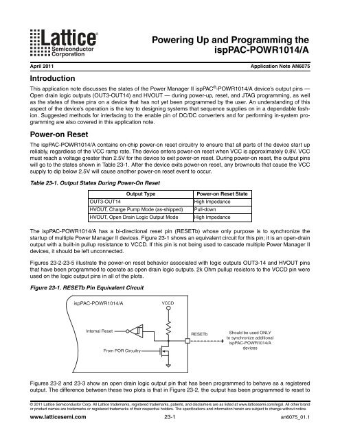
The <strong>ispPAC</strong>-<strong>POWR1014</strong>/A has a bi-directional reset pin (RESETb) whose only purpose is to synchronize <strong>the</strong><br />
startup of multiple Power Manager II devices. Figure 23-1 shows an equivalent circuit for this pin; it is an open-drain<br />
output with a built-in pullup resistance to VCCD. If this pin is not being used to cascade multiple Power Manager II<br />
devices, it should be left unconnected.<br />
Figures 23-2-23-5 illustrate <strong>the</strong> power-on reset behavior associated with logic outputs OUT3-14 <strong>and</strong> HVOUT pins<br />
that have been programmed to operate as open drain logic outputs. 2k Ohm pullup resistors to <strong>the</strong> VCCD pin were<br />
used on <strong>the</strong> logic output pins in all of <strong>the</strong> plots.<br />
Figure 23-1. RESETb Pin Equivalent Circuit<br />
Output Type Power-on Reset State<br />
OUT3-OUT14 High Impedance<br />
HVOUT, Charge Pump Mode (as-shipped) Pull-down<br />
HVOUT, Open Drain Logic Output Mode High Impedance<br />
<strong>ispPAC</strong>-<strong>POWR1014</strong>/A<br />
Internal Reset<br />
From POR Circuitry<br />
<strong>Powering</strong> <strong>Up</strong> <strong>and</strong> <strong>Programming</strong> <strong>the</strong><br />
<strong>ispPAC</strong>-<strong>POWR1014</strong>/A<br />
VCCD<br />
RESETb<br />
Should be used ONLY<br />
to synchronize additional<br />
<strong>ispPAC</strong>-<strong>POWR1014</strong>/A<br />
devices<br />
Figures 23-2 <strong>and</strong> 23-3 show an open drain logic output pin that has been programmed to behave as a registered<br />
output. The difference between <strong>the</strong>se two plots is that in Figure 23-2, <strong>the</strong> output has been programmed to reset to<br />
© 2011 <strong>Lattice</strong> Semiconductor Corp. All <strong>Lattice</strong> trademarks, registered trademarks, patents, <strong>and</strong> disclaimers are as listed at www.latticesemi.com/legal. All o<strong>the</strong>r br<strong>and</strong><br />
or product names are trademarks or registered trademarks of <strong>the</strong>ir respective holders. The specifications <strong>and</strong> information herein are subject to change without notice.<br />
www.latticesemi.com 23-1 an6075_01.1
<strong>Powering</strong> <strong>Up</strong> <strong>and</strong> <strong>Programming</strong><br />
<strong>Lattice</strong> Semiconductor <strong>the</strong> <strong>ispPAC</strong>-<strong>POWR1014</strong>/A<br />
a low level, whereas in Figure 23-3, it has been programmed to reset high. The power supply goes from zero to<br />
3.3V in 20 milliseconds. The waveforms in Figures 23-2 <strong>and</strong> 23-3 are typical of VCC supplies that take more than a<br />
millisecond to reach 3.3V.<br />
Figure 23-2. Startup with Slow Supply; Output Resets Low<br />
Figure 23-3. Startup with Slow Supply; Output Resets High<br />
The behavior in both cases is identical until <strong>the</strong> time that VCC reaches 2.5V. RESETb pulls down starting at a VCC<br />
voltage of 0.8V; <strong>the</strong> RESETb output thus follows VCC up until this point. The open drain logic output retains its high<br />
impedance state until VCC reaches 2.5V; <strong>the</strong> voltage observed at <strong>the</strong> open drain logic output thus follows VCC to<br />
2.5V. When VCC reaches 2.5V, power-on reset ends. From that point on, RESETb goes to a high level, <strong>and</strong> <strong>the</strong><br />
logic outputs assume <strong>the</strong>ir programmed macrocell reset levels.<br />
Figures 23-4 <strong>and</strong> 23-5 show <strong>the</strong> waveforms observed when <strong>the</strong> same device <strong>and</strong> setup that were examined in Figures<br />
23-2 <strong>and</strong> 23-3 are powered from a supply that goes from 0 to 3.3V in 100 microseconds. Despite <strong>the</strong> faster<br />
power-up rate, RESETb still indicates that power-on reset starts when VCC reaches 0.8V. At this faster power-up<br />
rate, however, <strong>the</strong> time at which power-on reset ends is dominated by <strong>the</strong> time that it takes for <strong>the</strong> logic circuitry<br />
inside <strong>the</strong> <strong>ispPAC</strong>-<strong>POWR1014</strong>/A device to initialize, ra<strong>the</strong>r than occurring when VCC crosses 2.5V. Regardless of<br />
<strong>the</strong> VCC supply ramp rate, <strong>the</strong> low-to-high transition of RESETb indicates that <strong>the</strong> logic circuitry is ready to operate,<br />
<strong>and</strong> <strong>the</strong> outputs can be observed going to <strong>the</strong>ir programmed states.<br />
23-2
<strong>Powering</strong> <strong>Up</strong> <strong>and</strong> <strong>Programming</strong><br />
<strong>Lattice</strong> Semiconductor <strong>the</strong> <strong>ispPAC</strong>-<strong>POWR1014</strong>/A<br />
Figure 23-4. Startup with Fast Supply; Output Resets Low<br />
Figure 23-5. Startup with Fast Supply; Output Resets High<br />
HVOUT pins that have been programmed for charge pump operation pull down during power-on reset regardless of<br />
<strong>the</strong> reset levels programmed into <strong>the</strong>ir associated macrocells. This is a safety feature that ensures that <strong>the</strong> external<br />
MOSFETs that <strong>the</strong>se pins control will be off when <strong>the</strong> <strong>ispPAC</strong>-<strong>POWR1014</strong>/A begins its power supply sequencing<br />
operations.<br />
An internal delayed reset signal, called AGOOD in PAC-Designer ® , becomes true approximately 220 microseconds<br />
after RESETb goes high. AGOOD is an indication that all analog circuitry in <strong>the</strong> device is ready. Since <strong>the</strong> logic circuitry<br />
becomes available before <strong>the</strong> analog circuitry, PAC-Designer’s LogiBuilder interface automatically inserts a<br />
“Wait for AGOOD” instruction at <strong>the</strong> beginning of each new sequence as a convenience. The user is given <strong>the</strong> freedom<br />
to insert new steps before <strong>the</strong> “Wait for AGOOD” instruction because sequencing tasks that depend purely on<br />
digital inputs can be performed before AGOOD becomes true.<br />
Because all VMON comparator outputs will be low, regardless of <strong>the</strong> voltage at <strong>the</strong> VMON input pin, before <strong>the</strong><br />
analog circuitry is ready, any supervisory logic window equations in which a low VMON comparator output indicates<br />
a failure condition will need to use AGOOD to block <strong>the</strong> comparator signal. For example, assume that two<br />
VMON inputs (Vin_5v <strong>and</strong> Vin_3v3) are being used to monitor rails not sequenced by this Power Manager device<br />
for brownout conditions <strong>and</strong> that if ei<strong>the</strong>r of <strong>the</strong>se rails browns out, <strong>the</strong> signal BROWN_OUT is to be driven low. If<br />
we program <strong>the</strong> supervisory logic equation<br />
23-3
<strong>Powering</strong> <strong>Up</strong> <strong>and</strong> <strong>Programming</strong><br />
<strong>Lattice</strong> Semiconductor <strong>the</strong> <strong>ispPAC</strong>-<strong>POWR1014</strong>/A<br />
BROWN_OUT = Vin_5v AND Vin_3v3<br />
<strong>the</strong> result will be that BROWN_OUT will pull low for about 220 microseconds following <strong>the</strong> release of RESETb,<br />
even if <strong>the</strong>se voltage rails are within acceptable limits during that time. Modifying <strong>the</strong> above equation to<br />
BROWN_OUT = (NOT AGOOD) OR (Vin_5v AND Vin_3v3)<br />
prevents an indication of failure from being generated due to <strong>the</strong> analog circuitry not being ready. During that time,<br />
<strong>the</strong> expression NOT AGOOD will be true, forcing <strong>the</strong> output BROWN_OUT to be high.<br />
User-initiated Resets<br />
The <strong>ispPAC</strong>-<strong>POWR1014</strong>/A may be reset via I 2 C or JTAG. CAUTION: The output pins will go to <strong>the</strong> states defined in<br />
Table 23-2 during a reset event, irrespective of <strong>the</strong> logic implemented.<br />
Table 23-2. Output States During Reset<br />
At <strong>the</strong> conclusion of <strong>the</strong> reset event, <strong>the</strong> RESETb pin goes high. The OUT3 to OUT14 pins, as well <strong>the</strong> HVOUT pins<br />
go to <strong>the</strong>ir programmed levels at this time. AGOOD becomes true approximately 220 microseconds after RESETb<br />
goes high. The VMON comparators become operational when AGOOD becomes true.<br />
Behavior During JTAG <strong>Programming</strong><br />
During JTAG programming, <strong>the</strong> RESETb pin goes to a low value, <strong>and</strong> <strong>the</strong> output pins go to <strong>the</strong> states defined in<br />
Table 23-3.<br />
Table 23-3. Output States During JTAG <strong>Programming</strong><br />
HVOUT pins that were programmed for open drain logic operation temporarily change to FET driver mode during<br />
programming <strong>and</strong> pull down. This behavior ensures that any MOSFETs driven by <strong>the</strong>se pins will stay off during programming.<br />
If <strong>the</strong> HVOUT pins are being used as open drain logic outputs, <strong>the</strong>n it is recommended that power be<br />
supplied only to <strong>the</strong> <strong>ispPAC</strong>-<strong>POWR1014</strong>/A through VCCJ <strong>and</strong> VCCPROG during in-system programming. Strategies<br />
for doing this are covered in a later section of this application note.<br />
Shipped State of New Parts<br />
Output Pin Reset State<br />
OUT3 to OUT14 High-Z<br />
HVOUT 1-2, FET Driver (as-shipped) Discharge<br />
HVOUT 1-2, Open-Drain High-Z<br />
Output Type State During JTAG <strong>Programming</strong><br />
OUT3 to OUT14 High Impedance<br />
HVOUT Pull-down<br />
<strong>ispPAC</strong>-<strong>POWR1014</strong>/A devices are programmed during factory testing with a sequence known as <strong>the</strong> “as-shipped”<br />
state. The output pins of devices in <strong>the</strong> as-shipped state will assume <strong>the</strong> states defined in Table 23-4 once poweron<br />
reset is completed. The I 2 C address of devices in <strong>the</strong> as-shipped state is 0.<br />
Table 23-4. Output Functions of Device As-Shipped from <strong>Lattice</strong> Semiconductor<br />
Output Pin As-Shipped State<br />
OUT3-14 High-Z<br />
HVOUT 1&2 Discharge (FET driver mode)<br />
MCLK High-Z (St<strong>and</strong>alone clocking mode)<br />
PLDCLK Enabled<br />
23-4
<strong>Powering</strong> <strong>Up</strong> <strong>and</strong> <strong>Programming</strong><br />
<strong>Lattice</strong> Semiconductor <strong>the</strong> <strong>ispPAC</strong>-<strong>POWR1014</strong>/A<br />
Ensuring Reliable Operation at Power-up<br />
Power supply systems using <strong>the</strong> <strong>ispPAC</strong>-<strong>POWR1014</strong>/A should be designed such that a high impedance state on a<br />
given logic output disables <strong>the</strong> supply controlled by that pin. Supplies with negative enable logic – that is, ones in<br />
which pulling <strong>the</strong> enable pin to ground turns <strong>the</strong> supply on – can often be connected directly to <strong>the</strong> open drain output<br />
pins without any additional components. For supplies with positive enable logic, <strong>the</strong> circuit in Figure 23-6 should<br />
be used. In both cases, <strong>the</strong> DC/DC converter data sheet should be checked to see whe<strong>the</strong>r its enable input has a<br />
built-in pullup resistor or whe<strong>the</strong>r an external resistor must be used. Tables 23-5 <strong>and</strong> 23-6 list <strong>the</strong> values that should<br />
be used in <strong>the</strong> LogiBuilder OUTPUT instructions <strong>and</strong> <strong>the</strong> reset levels that should be selected in <strong>the</strong> “PINS” window<br />
for supplies with positive <strong>and</strong> negative enable logic, respectively.<br />
Figure 23-6. Interfacing to Supplies with Positive Enable Logic<br />
<strong>ispPAC</strong>-<br />
<strong>POWR1014</strong>/A<br />
Table 23-5. Controlling Positive Logic Supplies<br />
Interface Method<br />
Use Inverter Circuit (Figure 23-<br />
6)<br />
Table 23-6. Controlling Negative Logic Supplies<br />
Interface Method<br />
Connect Directly to Open-Drain<br />
Output<br />
Open drain output<br />
“PINS” Window<br />
Reset Level<br />
LogiBuilder OUTPUT Value<br />
to Turn Supply ON<br />
In-System <strong>Programming</strong> with <strong>the</strong> <strong>ispPAC</strong>-<strong>POWR1014</strong>/A<br />
The <strong>ispPAC</strong>-<strong>POWR1014</strong>/A provides several different modes of programming, in relation to how it is powered. Using<br />
<strong>the</strong> st<strong>and</strong>ard method of powering VCCD, VCCA <strong>and</strong> VCCJ, <strong>the</strong> device can be programmed as powered up normally<br />
<strong>and</strong> <strong>the</strong> device output pins will respond to <strong>the</strong> programming as noted in Table 23-3. After <strong>the</strong> program is complete,<br />
<strong>the</strong> device is ready to start its sequence.<br />
The second method is for programming just <strong>the</strong> <strong>ispPAC</strong>-<strong>POWR1014</strong>/A, without powering up <strong>the</strong> PLD macrocells,<br />
I/O or I 2 C circuitry. This method allows <strong>the</strong> user to power up just a portion of <strong>the</strong> device for programming without<br />
powering up <strong>the</strong> whole board or affecting o<strong>the</strong>r devices <strong>and</strong> supplies in <strong>the</strong> system. This is achieved by powering<br />
VCCPROG <strong>and</strong> VCCJ only. A simple low power external 3.3V supply is needed to supply power to VCCPROG <strong>and</strong><br />
VCCJ as shown in Figure 23-7. In this mode <strong>the</strong> HVOUT pins will be low <strong>and</strong> <strong>the</strong> OUT3-OUT14 will be in a high<br />
23-5<br />
LogiBuilder OUTPUT Value<br />
to Turn Supply OFF<br />
HIGH 0 (Deassert) 1 (Assert)<br />
“PINS” Window<br />
Reset Level<br />
10k<br />
DC/DC Converter<br />
Input Supply<br />
10k*<br />
PN2222A or<br />
equivalent<br />
* Required only if <strong>the</strong> DC-DC converter does not<br />
have an internal pull-up resistance.<br />
LogiBuilder OUTPUT Value<br />
to Turn Supply ON<br />
DC/DC Converter<br />
ENABLE<br />
LogiBuilder OUTPUT Value<br />
to Turn Supply OFF<br />
HIGH 0 (Deassert) 1 (Assert)
<strong>Powering</strong> <strong>Up</strong> <strong>and</strong> <strong>Programming</strong><br />
<strong>Lattice</strong> Semiconductor <strong>the</strong> <strong>ispPAC</strong>-<strong>POWR1014</strong>/A<br />
impedance state. Once programming is complete, remove <strong>the</strong> VCCPROG supply <strong>and</strong> power up with VCCA, VCCD,<br />
<strong>and</strong> VCCINP. To enable normal JTAG operations, power should be applied to VCCJ <strong>and</strong> can be separated from<br />
VCCPROG with a jumper or Schottky diode.<br />
Figure 23-7. <strong>Powering</strong> Through VCCPROG <strong>and</strong> VCCJ During <strong>Programming</strong><br />
JTAG <strong>Programming</strong> Cable or<br />
Test Points<br />
<strong>Programming</strong><br />
VCC Supply<br />
+3.3V<br />
TDI<br />
TDO<br />
TMS<br />
TCK<br />
GND<br />
N/C<br />
To have <strong>the</strong> device fully powered up during programming, power should be applied to VCCJ, VCCD, <strong>and</strong> VCCA, but<br />
not VCCPROG. This is <strong>the</strong> strategy that must be used if it is desired to initiate a test sequence via JTAG (by writing<br />
to <strong>the</strong> register associated with IN1) after programming is complete. Frequently, o<strong>the</strong>r JTAG devices on <strong>the</strong> board,<br />
such as FPGAs, have <strong>the</strong>ir power sequenced on by <strong>the</strong> <strong>ispPAC</strong>-<strong>POWR1014</strong>/A. Ideally, <strong>the</strong> design should be<br />
achievable using only one JTAG chain. The <strong>ispPAC</strong>-<strong>POWR1014</strong>/A provides an alternate TDI JTAG input feature<br />
that makes this goal achievable. By using <strong>the</strong> ATDI pin, as shown in Figure 8, <strong>the</strong> unpowered devices in <strong>the</strong> chain<br />
can be bypassed while <strong>the</strong> <strong>ispPAC</strong>-<strong>POWR1014</strong>/A is being programmed. TDISEL should be pulled to ground during<br />
programming of <strong>the</strong> Power Manager II device in order to select <strong>the</strong> ATDI input. All JTAG devices in <strong>the</strong> chain must<br />
be hot-socket compatible to guarantee that <strong>the</strong> TMS <strong>and</strong> TCK signals are not clamped. For a more detailed treatment<br />
on programming using <strong>the</strong> ATDI input, please refer to AN6068, <strong>Programming</strong> <strong>the</strong> <strong>ispPAC</strong>-POWR1220AT8 in a<br />
JTAG Chain Using <strong>the</strong> ATDI Pin. The operation of <strong>the</strong> ATDI feature on <strong>the</strong> <strong>ispPAC</strong>-<strong>POWR1014</strong>/A is identical to that<br />
on <strong>the</strong> <strong>ispPAC</strong>-POWR1220AT8.<br />
23-6<br />
TDISEL<br />
VCCJ<br />
VCCPROG<br />
TDI<br />
TDO<br />
TMS<br />
TCK<br />
GNDA<br />
Main +3.3V Supply (Not active<br />
during JTAG programming)<br />
<strong>ispPAC</strong>-<strong>POWR1014</strong>/A<br />
GNDD<br />
VCCA<br />
VCCD
<strong>Powering</strong> <strong>Up</strong> <strong>and</strong> <strong>Programming</strong><br />
<strong>Lattice</strong> Semiconductor <strong>the</strong> <strong>ispPAC</strong>-<strong>POWR1014</strong>/A<br />
Figure 23-8. Using ATDI to Bypass Unpowered Devices<br />
TDISEL<br />
TDI<br />
TCK<br />
TMS<br />
TDO<br />
Non hot-socket compliant devices may share a JTAG chain with <strong>the</strong> <strong>ispPAC</strong>-<strong>POWR1014</strong>/A if <strong>the</strong>se devices have a<br />
separate VCCJ power supply pin. Power must be applied to <strong>the</strong> VCCJ pins on <strong>the</strong>se devices while programming<br />
<strong>the</strong> <strong>ispPAC</strong>-<strong>POWR1014</strong>/A in order to prevent clamping of <strong>the</strong> TMS <strong>and</strong> TCK signals. These devices can be<br />
bypassed by using <strong>the</strong> ATDI feature.<br />
Capacitive Loading on Outputs<br />
In certain applications, <strong>the</strong> outputs of <strong>the</strong> Power Manager device are used to enable <strong>the</strong> soft-start feature of a DC-<br />
DC converter. This presents a capacitive load to <strong>the</strong> outputs of <strong>the</strong> Power Manager. During <strong>the</strong> power-up cycle of<br />
<strong>the</strong> Power Manager, <strong>the</strong> open-drain outputs will transition from active low to high-z. Likewise, <strong>the</strong> HVOUT pins will<br />
transition from active low to discharge (or high-z depending on <strong>the</strong> configuration) during <strong>the</strong> power-up cycle. If <strong>the</strong><br />
soft-start capacitors have any charge stored during this time, excessive currents will flow through <strong>the</strong> open-drain<br />
outputs to ground. These currents can result in an unreliable start-up of <strong>the</strong> Power Manager. Fur<strong>the</strong>rmore, during<br />
normal operation setting an output low can also result in a discharge current that exceeds <strong>the</strong> maximum current<br />
limits in <strong>the</strong> data sheet.<br />
To ensure reliable Power Manager start-up <strong>and</strong> to limit <strong>the</strong> current surge it is required to add a series resistor when<br />
a capacitive load is connected to an output as shown in Figure 23-9. The value of R1 should be such that when C1<br />
is discharged by <strong>the</strong> open-drain output <strong>the</strong> current is less than <strong>the</strong> ISINKMAXTOTAL limit in <strong>the</strong> data sheet. The ISINKMAX-<br />
TOTAL is for any single output <strong>and</strong> is found in <strong>the</strong> Absolute Maximum Ratings Table of <strong>the</strong> data sheet. If multiple outputs<br />
have capacitive loads <strong>the</strong> ISINKTOTAL Max should also be considered in setting a value for <strong>the</strong> series resistors.<br />
The ISINKTOTAL number is found in <strong>the</strong> Digital Specifications table of <strong>the</strong> data sheet <strong>and</strong> applies to all outputs combined.<br />
23-7<br />
Power Supplies<br />
VCC<br />
VCC<br />
HVOUT VCC<br />
JTAG<br />
Device 1<br />
JTAG<br />
Device 2<br />
<strong>ispPAC</strong>-POWR<br />
1014/A<br />
TDI<br />
TDI TDO TDI TDO<br />
TDISEL TDO<br />
TCK TMS TCK TMS<br />
ATDI TCK TMS
<strong>Powering</strong> <strong>Up</strong> <strong>and</strong> <strong>Programming</strong><br />
<strong>Lattice</strong> Semiconductor <strong>the</strong> <strong>ispPAC</strong>-<strong>POWR1014</strong>/A<br />
Figure 23-9. Limiting Capacitive Load Currents to Less than ISINKMAXTOTAL<br />
Summary<br />
The startup characteristics of <strong>the</strong> open drain logic outputs (OUT3 to OUT14) <strong>and</strong> <strong>the</strong> HVOUT pins as a function of<br />
<strong>the</strong> power-on reset condition have been described. The behavior of <strong>the</strong>se outputs has also been defined during<br />
user-issued resets <strong>and</strong> during JTAG programming. The programmed state in which new devices are shipped from<br />
<strong>the</strong> factory (<strong>the</strong> “as-shipped” state) has been described.<br />
To ensure reliable startup of power supplies, <strong>the</strong> <strong>ispPAC</strong>-<strong>POWR1014</strong>/A’s logic outputs should be set up so that a<br />
logic low activates <strong>the</strong> supplies. Supplies that use positive enable logic require a simple one-transistor inverter to<br />
interface to <strong>the</strong> <strong>ispPAC</strong>-<strong>POWR1014</strong>/A’s open drain logic outputs.<br />
Strategies to perform in-system programming by applying power only to VCCJ <strong>and</strong> VCCPROG are strongly suggested.<br />
An example was presented showing a system in which <strong>the</strong> <strong>ispPAC</strong>-<strong>POWR1014</strong>/As JTAG interface is<br />
shared between a JTAG programmer <strong>and</strong> an on-board JTAG chain that uses <strong>the</strong> device’s non-programming JTAG<br />
capabilities.<br />
When outputs are driving a capacitive load a series resistor is required to insure <strong>the</strong> discharge current is below <strong>the</strong><br />
current limits in <strong>the</strong> data sheet.<br />
Related Literature<br />
<strong>ispPAC</strong>-<strong>POWR1014</strong>/A Data Sheet<br />
AN6068, <strong>Programming</strong> <strong>the</strong> <strong>ispPAC</strong>-POWR1220AT8 in a JTAG Chain Using <strong>the</strong> ATDI Pin<br />
Technical Support Assistance<br />
Hotline: 1-800-LATTICE (North America)<br />
+1-503-268-8001 (Outside North America)<br />
e-mail: isppacs@latticesemi.com<br />
Internet: www.latticesemi.com<br />
Revision History<br />
Power Manager<br />
R1<br />
C1<br />
DC/DC Converter<br />
Input Supply<br />
Date Version Change Summary<br />
March 2006 01.0 Initial release.<br />
April 2011 01.1 <strong>Up</strong>dated to address capacitive loading on <strong>the</strong> outputs.<br />
23-8<br />
Soft-Start<br />
Enable<br />
DC-DC Converter