TN1050 - Lattice Semiconductor
TN1050 - Lattice Semiconductor
TN1050 - Lattice Semiconductor

Create successful ePaper yourself
Turn your PDF publications into a flip-book with our unique Google optimized e-Paper software.
September 2012 Technical Note <strong>TN1050</strong><br />
Introduction<br />
<strong>Lattice</strong>ECP, <strong>Lattice</strong>EC and <strong>Lattice</strong>XP devices support various Double Data Rate (DDR) and Single Data<br />
Rate (SDR) interfaces using the logic built into the Programmable I/O (PIO). SDR applications capture data on one<br />
edge of a clock while the DDR interfaces capture data on both the rising and falling edges of the clock, thus doubling<br />
the performance. This document will address in detail how to utilize the capabilities of the <strong>Lattice</strong>ECP/EC and<br />
<strong>Lattice</strong>XP devices to implement both generic DDR and DDR memory interfaces.<br />
DDR SDRAM Interfaces Overview<br />
DDR SDRAM interfaces rely on the use of a data strobe signal, called DQS, for high-speed operation. When reading<br />
data from the external memory device, data coming into the device is edge aligned with respect to the DQS signal.<br />
This DQS strobe signal needs to be phase shifted 90 degrees before FPGA logic can sample the read data.<br />
When writing to a DDR SDRAM the memory controller (FPGA) must shift the DQS by 90 degrees to center align<br />
with the data signals (DQ). DQ and DQS are bi-directional ports. The same two signals are used for both write and<br />
read operations. A clock signal is also provided to the memory. This clock is provided as a differential clock (CLKP<br />
and CLKN) to minimize duty cycle variations. The memory also uses these clock signals to generate the DQS signal<br />
during a read via a DLL inside the memory. The skew between CLKP or CLKN and the SDRAM-generated<br />
DQS signal is specified in the DDR SDRAM data sheet. Figures 10-1 and 10-2 show DQ and DQS relationships for<br />
read and write cycles.<br />
During read, the DQS signal is LOW for some duration after it comes out of tristate. This state is called Preamble.<br />
The state when the DQS is LOW before it goes into Tristate is the Postamble state. This is the state after the last<br />
valid data transition.<br />
DDR SDRAM also require a Data Mask (DM) signals to mask data bits during write cycles. SDRAM interfaces typically<br />
are implemented with x8, x16 and x32 bits for each DQS signal. Note that the ratio of DQS to data bits is<br />
independent of the overall width of the memory. An 8-bit interface will have one strobe signal.<br />
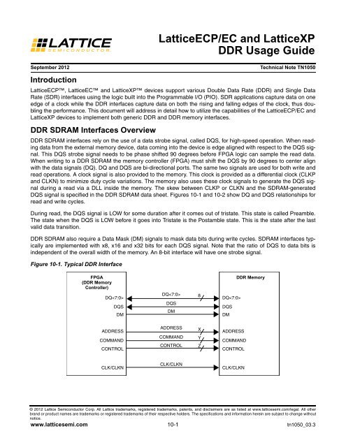
Figure 10-1. Typical DDR Interface<br />
FPGA<br />
(DDR Memory<br />
Controller)<br />
DQ<br />
DQS<br />
DM<br />
ADDRESS<br />
COMMAND<br />
CONTROL<br />
CLK/CLKN<br />
<strong>Lattice</strong>ECP/EC and <strong>Lattice</strong>XP<br />
DDR Usage Guide<br />
DQ<br />
DQS<br />
DM<br />
ADDRESS<br />
COMMAND<br />
CONTROL<br />
CLK/CLKN<br />
DQ<br />
DDR Memory<br />
© 2012 <strong>Lattice</strong> <strong>Semiconductor</strong> Corp. All <strong>Lattice</strong> trademarks, registered trademarks, patents, and disclaimers are as listed at www.latticesemi.com/legal. All other<br />
brand or product names are trademarks or registered trademarks of their respective holders. The specifications and information herein are subject to change without<br />
notice.<br />
www.latticesemi.com 10-1 tn1050_03.3<br />
8<br />
X<br />
Y<br />
Z<br />
DQS<br />
DM<br />
ADDRESS<br />
COMMAND<br />
CONTROL<br />
CLK/CLKN
Figure 10-2. DQ-DQS During READ<br />
Figure 10-3. DQ-DQS During WRITE<br />
DQS<br />
(at PIN)<br />
DQ<br />
(at PIN)<br />
10-2<br />
<strong>Lattice</strong>ECP/EC and <strong>Lattice</strong>XP<br />
DDR Usage Guide<br />
Implementing DDR Memory Interfaces with the <strong>Lattice</strong>ECP/EC Devices<br />
This section describes how to implement the read and write sections of a DDR memory interface. It also provides<br />
details of the DQ and DQS grouping rules associated with the <strong>Lattice</strong>ECP/EC and <strong>Lattice</strong>XP devices.<br />
DQS Grouping<br />
DQS<br />
(at PIN) Preamble Postamble<br />
DQ<br />
(at PIN)<br />
DQS<br />
(at REG)<br />
DQ<br />
(at REG)<br />
DQS PIN to<br />
REG and 90<br />
Degree<br />
Phase Shift<br />
Each DQS group generally consists of at least 10 I/Os (1DQS, 8DQ and 1DM) to implement a complete 8-bit DDR<br />
memory interface. In the <strong>Lattice</strong>ECP/EC devices each DQS signal will span across 16 I/Os and in the <strong>Lattice</strong>XP<br />
devices the DQS will span 14 I/Os. Any 10 of these 16 I/Os can be used to implement an 8-bit DDR memory interface.<br />
In addition to the DQS grouping, the user must also assign one reference voltage VREF1 for a given I/O bank.<br />
The tables below show the total number of DQS groups available per I/O bank for each device and package.
Table 10-1. Number of DQS Banks in the <strong>Lattice</strong>ECP/EC Device<br />
Package Device<br />
100-pin TQFP<br />
144-pin TQFP<br />
208-pin TQFP<br />
256-ball fpBGA<br />
484-ball fpBGA<br />
Total x8<br />
DQS Groups<br />
Table 10-2. Number of DQS Banks in the <strong>Lattice</strong>XP Device<br />
10-3<br />
<strong>Lattice</strong>ECP/EC and <strong>Lattice</strong>XP<br />
DDR Usage Guide<br />
Number of DQS Groups per I/O Bank<br />
0 1 2 3 4 5 6 7<br />
LFEC1 3 1 1 0 0 1 0 0 0<br />
LFEC3 3 1 1 0 0 1 0 0 0<br />
LFEC1 6 1 1 0 1 1 1 1 0<br />
LFEC3 6 1 1 0 1 1 1 1 0<br />
LFEC6/LFECP6 6 1 1 0 1 1 1 1 0<br />
LFEC1 6 1 1 0 1 1 1 1 0<br />
LFEC3 8+21 1+1 1<br />
1 1 1 1 1+1 1<br />
1 1<br />
LFEC6/LFECP6 8+21 1+1 1<br />
1 1 1 1 1+1 1<br />
1 1<br />
LFEC10/LFECP10 8+2 1<br />
1+1 1<br />
1 1 1 1 1+1 1<br />
1 1<br />
LFEC3 10 2 1 1 1 1 2 1 1<br />
LFEC6/LFECP6 12 2 1 1 2 1 2 2 1<br />
LFEC10/LFECP10 12 2 1 1 2 1 2 2 1<br />
LFEC15/LFECP15 12 2 1 1 2 1 2 2 1<br />
LFEC6/LFECP6 14 2 2 1 2 2 2 2 1<br />
LFEC10/LFECP10 18 3 2 2 2 2 3 2 2<br />
LFEC15/LFECP15 20 3 3 2 2 3 3 2 2<br />
LFEC20/LFECP20 22 3 3 2 3 3 3 3 2<br />
LFEC33/LFECP33 22 3 3 2 3 3 3 3 2<br />
LFEC20/LFECP20 24 4 3 2 3 3 4 3 2<br />
672-ball fpBGA<br />
LFEC33/LFECP33 30 4 4 3 4 4 4 4 3<br />
1. 10 I/Os (1 DQS + 8 DQs + Bank VREF1) can function as a DDR interface in which the FPGA can have a DM output but not a DQS aligned<br />
input (in the same DDR bank as the rest of the system).<br />
Package Device<br />
100-pin TQFP<br />
144-pin TQFP<br />
208-pin PQFP<br />
256-ball fpBGA<br />
388-ball fpBGA<br />
Total x8<br />
DQS Groups<br />
Number of DQS Groups per I/O Bank<br />
0 1 2 3 4 5 6 7<br />
LFXP3C/LFXP3E 2 0 0 0 0 0 1 0 1<br />
LFXP6C LFXP6E 2 0 0 0 0 0 1 0 1<br />
LFXP3C/LFXP3E 7 1 0 1 1 1 1 1 1<br />
LFXP6C/LFXP6E 7 1 0 1 1 1 1 1 1<br />
LFXP3C/LFXP3E 8 1 1 1 1 1 1 1 1<br />
LFXP6C/LFXP6E 8 1 1 1 1 1 1 1 1<br />
LFXP3C/LFXP3E 12 2 2 1 1 2 2 1 1<br />
LFXP6C/LFXP6E 12 2 2 1 1 2 2 1 1<br />
LFXP10C/LFXP10E 16 2 2 2 2 2 2 2 2<br />
LFXP15C/LFXP15E 16 2 2 2 2 2 2 2 2<br />
LFXP20C/LFXP20E 20 3 3 2 2 3 3 2 2<br />
LFXP10C/LFXP10E 16 2 2 2 2 2 2 2 2<br />
LFXP15C/LFXP15E 20 3 3 2 2 3 3 2 2<br />
LFXP20C/LFXP20E 20 3 3 2 2 3 3 2 2<br />
484-ball fpBGA<br />
LFXP15C/LFXP15E<br />
LFXP20C/LFXP20E<br />
20<br />
20<br />
3<br />
3<br />
3<br />
3<br />
2<br />
2<br />
2<br />
2<br />
3<br />
3<br />
3<br />
3<br />
2<br />
2<br />
2<br />
2<br />
672-ball fpBGA LFXP20C/LFXP20E 24 4 4 2 2 4 4 2 2
Figure 10-4. DQ-DQS Grouping<br />
n* I/O PADS<br />
DQS PAD<br />
(Ninth I/O Pad)<br />
*For <strong>Lattice</strong>ECP/EC: n = 16, for <strong>Lattice</strong>XP: n = 14.<br />
10-4<br />
DQ, DM or VREF1<br />
<strong>Lattice</strong>ECP/EC and <strong>Lattice</strong>XP<br />
DDR Usage Guide<br />
Figure 10-4 shows a typical DQ-DQS group for both the <strong>Lattice</strong>ECP/EC device and the <strong>Lattice</strong>XP device. The ninth<br />
I/O of this group of 16 I/Os (for <strong>Lattice</strong>ECP/EC) or 14 I/Os (for <strong>Lattice</strong>XP) is the dedicated DQS pin. All eight pads<br />
before the DQS and seven (for <strong>Lattice</strong>ECP/EC) or four (for <strong>Lattice</strong>XP) pads after the DQS are covered by this DQS<br />
bus span. The user can assign any eight of these I/O pads to be DQ data pins. Hence, to implement a 32-bit wide<br />
memory interface you would need to use four such DQ-DQS groups.<br />
When not interfacing with the memory, the dedicated DQS pin can be used as a general purpose I/O. Each of the<br />
dedicated DQS pin is internally connected to the DQS phase shift circuitry. The pinout information contained in the<br />
<strong>Lattice</strong>ECP/EC and <strong>Lattice</strong>XP device data sheets shows pin locations for the DQS pads. Table 10-2 shows an<br />
extract from the <strong>Lattice</strong>ECP/EC data sheet. In this case, the DQS is marked as LDQS6 (L=left side, 6 =associated<br />
PFU row/column). Since DQS is always the fifth true pad in the DQ-DQS group, counting from low to high PFU<br />
row/column number, LDQS6 will cover PL2A to PL9B. Following this convention, there are eight pads before and<br />
seven pads after DQS for DQ available following counter-clockwise for the left and bottom sides of the device, and<br />
following clockwise for the top and right sides of the device. The user can assign any eight of these pads to be DQ<br />
data signals. The <strong>Lattice</strong>XP device follows the same method.<br />
Table 10-3. EC20 Pinout (from <strong>Lattice</strong>ECP/EC Family Data Sheet)<br />
Ball Function Bank LVDS Dual Function 484 fpBGA 672 fpBGA<br />
PL2A 7 T VREF2_7 D4 E3<br />
PL2B 7 C VREF1_7 E4 E4<br />
PL3A 7 T — C3 B1<br />
PL3B 7 C — B2 C1<br />
PL4A 7 T — E5 F3<br />
PL4B 7 C — F5 G3<br />
PL5A 7 T — D3 D2<br />
PL5B 7 C — C2 E2<br />
PL6A 7 T LDQS6 F4 D1<br />
PL6B 7 C — G4 E1<br />
PL7A 7 T — E3 F2<br />
PL7B 7 C — D2 G2<br />
PL8A 7 T LUM0_PLLT_IN_A B1 F6<br />
PL8B 7 C LUM0_PLLC_IN_A C1 G6<br />
PL9A 7 T LUM0_PLLT_FB_A F3 H4<br />
PL9B 7 C LUM0_PLLC_FB_A E2 G4<br />
PL11A 7 T — G5 J4
Table 10-3. EC20 Pinout (from <strong>Lattice</strong>ECP/EC Family Data Sheet)<br />
DDR Software Primitives<br />
10-5<br />
<strong>Lattice</strong>ECP/EC and <strong>Lattice</strong>XP<br />
DDR Usage Guide<br />
Ball Function Bank LVDS Dual Function 484 fpBGA 672 fpBGA<br />
PL11B 7 C — H6 J5<br />
PL12A 7 T — G3 K4<br />
This section describes the software primitives that can be used to implement DDR interfaces and provides details<br />
about how to instantiate them in the software. The primitives described include:<br />
DQSDLL The DQS delay calibration DLL<br />
DQSBUF The DQS delay function and the clock polarity selection logic<br />
INDDRXB The DDR input and DQS to system clock transfer registers<br />
ODDRXB The DDR output registers<br />
An HDL usage example for each of these primitives is listed in Appendices B and C.<br />
DQSDLL<br />
The DQSDLL will generate a 90-degree phase shift required for the DQS signal. This primitive will implement the<br />
on-chip DQSDLL. Only one DQSDLL should be instantiated for all the DDR implementations on one half of the<br />
device. The clock input to this DLL should be at the same frequency as the DDR interface. The DLL will generate<br />
the delay based on this clock frequency and the update control input to this block. The DLL will update the dynamic<br />
delay control to the DQS delay block when this update control (UDDCNTL) input is asserted. Figure 10-5 shows<br />
the primitive symbol. The active low signal on UDDCNTL updates the DQS phase alignment and should be initiated<br />
at the beginning of READ cycles.<br />
Figure 10-5. DQSDLL Symbol<br />
Table 10-4 provides a description of the ports.<br />
Table 10-4. DQSDLL Ports<br />
CLK<br />
RST<br />
UDDCNTL<br />
DQSDLL<br />
Port Name I/O Definition<br />
CLK I System CLK should be at frequency of the DDR interface, from the FPGA core.<br />
RST I Resets the DQSDLL<br />
UDDCNTL<br />
I<br />
Provides an update signal to the DLL that will update the dynamic delay. When held low<br />
this signal will update the DQSDEL.<br />
LOCK O Indicates when the DLL is in phase<br />
DQSDEL O The digital delay generated by the DLL should be connected to the DQSBUF primitive.<br />
DQSDLL Configuration Attributes<br />
By default this DLL will generate a 90-degree phase shift for the DQS strobe based on the frequency of the input<br />
reference clock to the DLL. The user can control the sensitivity to jitter by using the LOCK_SENSITIVITY attribute.<br />
This configuration bit can be programmed to be either “HIGH” or “LOW”.<br />
LOCK<br />
DQSDEL
10-6<br />
<strong>Lattice</strong>ECP/EC and <strong>Lattice</strong>XP<br />
DDR Usage Guide<br />
The DLL Lock Detect circuit has two modes of operation controlled by the LOCK_SENSITIVITY bit, which selects<br />
more or less sensitivity to jitter. If this DLL is operated at or above 150 MHz, it is recommended that the<br />
LOCK_SENSITIVITY bit be programmed “HIGH” (more sensitive). For operation running at or under 100 MHz it is<br />
recommended that the bit be programmed “LOW” (more tolerant). For 133 MHz, the LOCK_SENSITIVITY bit can<br />
go either way.<br />
DQSBUF<br />
This primitive implements the DQS Delay and the DQS transition detector logic. Figure 10-6 shows the DQSBUFB<br />
function. The preamble detect signal is also generated within this primitive.<br />
Figure 10-6. DQSBUFB Function<br />
DQSI<br />
READ<br />
CLK<br />
V REF<br />
Figure 10-7 shows the primitive symbol and its ports. DQSI is the DQS signal from the memory. PRMBDET is the<br />
preamble detect signal that is generated from the DQSI input. READ and CLK are user interface signals coming<br />
from the FPGA logic. The DQSDLL block sends digital control line DQSDEL to this block. The DQS is delayed<br />
based on this input from the DQSDLL. DQSO is the delayed DQS and is connected to the clock input of the first set<br />
of DDR registers.<br />
Figure 10-7. DQSBUFB Symbol<br />
+<br />
-<br />
+<br />
-<br />
VREF - DV<br />
(DV ~ 170mV)<br />
PRMBDET<br />
DQSBUFB<br />
DQSI<br />
CLK<br />
READ<br />
DQSDEL<br />
DQSBUFB<br />
DQSDEL<br />
DQSDEL<br />
DQS<br />
TRANSITION<br />
DETECT<br />
DQSO<br />
DDRCLKPOL<br />
DQSC<br />
PRMBDET<br />
Table 10-5 provides a description of the I/O ports associated with the DQSBUFB primitive.<br />
DQSO<br />
DQSC<br />
PRMBDET<br />
DDRCLKPOL
Table 10-5. DQSBUFB Ports<br />
Notes:<br />
10-7<br />
<strong>Lattice</strong>ECP/EC and <strong>Lattice</strong>XP<br />
DDR Usage Guide<br />
Port Name I/O Definition<br />
DQSI I DQS strobe signal from memory<br />
CLK I System CLK<br />
READ I Read generated from the FPGA core<br />
DQSDEL I DQS delay from the DQSDLL primitive<br />
DQSO O Delayed DQS Strobe signal, to the input capture register block<br />
DQSC O DQS Strobe signal before delay, going to the FPGA core logic<br />
DDRCLKPOL O DDR Clock Polarity signal<br />
PRMBDET O Preamble detect signal, going to the FPGA core logic<br />
1. The DDR Clock Polarity output from this block should be connected to the DDCLKPOL inputs of the input<br />
register blocks (IDDRXB).<br />
READ Pulse Generation<br />
The READ signal to the DQSBUFB block is internally generated in the FPGA core. The Read signal will go high<br />
when the READ command to control the DDR SDRAM is initially asserted. This should normally precede the DQS<br />
preamble by one cycle yet may overlap the trailing bits of a prior read cycle. The DQS Detect circuitry of the <strong>Lattice</strong>ECP/EC<br />
and <strong>Lattice</strong>XP devices require the falling edge of the READ signal to be placed within the preamble<br />
stage.<br />
The preamble state of the DQS can be detected using the CAS latency and the round trip delay for the signals<br />
between the FPGA and the memory device. Note that the internal FPGA core generates the READ pulse. The rise<br />
of the READ pulse needs to coincide with the initial READ Command of the Read Burst and needs to go low before<br />
the Preamble goes high.<br />
Figure 10-8 shows the READ Pulse Timing Example with respect to the PRMBDET signal.<br />
Figure 10-8. READ Pulse Generation<br />
OK<br />
FAIL<br />
FAIL<br />
OK<br />
DQS<br />
PRMBDET<br />
READ<br />
READ<br />
READ<br />
READ<br />
PRIOR READ CYCLE<br />
POSTAMBLE<br />
PREAMBLE<br />
VTH<br />
FIRST DQS<br />
TRANSITION<br />
POSTAMBLE
10-8<br />
<strong>Lattice</strong>ECP/EC and <strong>Lattice</strong>XP<br />
DDR Usage Guide<br />
IDDRXB<br />
This primitive will implement the input register block. The software defaults to CE Enabled unless otherwise specified.<br />
The ECLK input is used to connect to the DQS strobe coming from the DQS delay block (DQSBUFB primitive).<br />
The SCLK input should be connected to the system (FPGA) clock. The SCLK and CE inputs to this primitive<br />
will be used primarily to synchronize the DDR inputs. DDRCLKPOL is an input from the DQS Clock Polarity tree.<br />
This signal is generated by the DQS Transition detect circuit in the hardware. Figure 10-9 shows the primitive symbol<br />
and the I/O ports.<br />
Figure 10-9. IDDRXB Symbol<br />
Table 10-6 provides a description of all I/O ports associated with the IDDRXB primitive.<br />
Table 10-6. IDDRXB Ports<br />
Note:<br />
D<br />
ECLK<br />
LSR<br />
IDDRXB<br />
SCLK<br />
CE<br />
DDRCLKPOL<br />
Port Name I/O Definition<br />
D I DDR data<br />
ECLK I The phase shifted DQS should be connected to this input<br />
LSR I Reset<br />
SCLK I System CLK<br />
CE I Clock enable<br />
DDRCLKPOL I DDR clock polarity signal<br />
QA O Data at the positive edge of the CLK<br />
QB O Data at the negative edge of the CLK<br />
1. The DDRCLKPOL input to IDDRXB should be connected to the DDRCLKPOL output of DQSBUFB.<br />
ODDRXB<br />
The ODDRXB primitive implements both the write and the tristate functions. This primitive is used to output DDR<br />
data and the DQS strobe to the memory. The CKP and CKN can also be generated using this primitive. All the<br />
DDR output tristate implementations are also implemented using the same primitive.<br />
Figure 10-10 shows the ODDRXB primitive symbol and its I/O ports.<br />
QA<br />
QB
Figure 10-10. ODDRXB Symbol<br />
Table 10-7 provides a description of all I/O ports associated with the ODDRXB primitive.<br />
Table 10-7. ODDRXB Ports<br />
Notes:<br />
10-9<br />
<strong>Lattice</strong>ECP/EC and <strong>Lattice</strong>XP<br />
DDR Usage Guide<br />
1. LSR should be held low during DDR Write operation. By default, the software will be implemented CE High<br />
and LSR low.<br />
2. DDR output and tristate registers do not have CE support. LSR is available for the tristate DDRX mode<br />
(while reading). The LSR will default to set when used in the tristate mode.<br />
3. CE and LSR support is available for the regular (non-DDR) output mode.<br />
4. When asserting reset during DDR writes, it is important to keep in mind that this would only reset the FFs<br />
and not the latches.<br />
Memory Read Implementation<br />
Port Name I/O Definition<br />
CLK I System CLK<br />
DA I Data at the positive edge of the clock<br />
DB I Data at the negative edge of the clock<br />
LSR I Reset<br />
Q I DDR data to the memory<br />
The <strong>Lattice</strong>ECP/EC and <strong>Lattice</strong>XP devices contain a variety of features to simplify implementation of the read portion<br />
of a DDR interface:<br />
DLL compensated DQS delay elements<br />
DDR input registers<br />
Automatic DQS to system clock domain transfer circuitry<br />
The <strong>Lattice</strong>ECP/EC and <strong>Lattice</strong>XP device data sheets detail these circuit elements.<br />
CLK<br />
DA<br />
DB<br />
LSR<br />
ODDRXB<br />
Three primitives in the <strong>Lattice</strong> ispLEVER ® design tools represent the capability of these three elements. The DQS-<br />
DLL represents the DLL used for calibration. The IDDRXB primitive represents the DDR input registers and clock<br />
domain transfer registers. Finally, the DQSBUFB represents the DQS delay block and the clock polarity control<br />
logic. These primitives are explained in more detail in the following sections of this document. Figure 10-11 illustrates<br />
how to hook these primitives together to implement the read portion of a DDR memory interface. The DDR<br />
Software Primitives section describes each of the primitives and its instantiation in more detail. Appendices A and B<br />
provide example code to implement the complete I/O section of a memory interface within a <strong>Lattice</strong>ECP/EC or <strong>Lattice</strong>XP<br />
device.<br />
Q
Figure 10-11. Software Primitive Implementation for Memory READ<br />
dq<br />
dqs<br />
clk<br />
read<br />
reset<br />
uddcntl<br />
ce<br />
DQSI<br />
CLK<br />
READ<br />
DQSBUFB<br />
6<br />
DQSDEL<br />
RST<br />
UDDCNTL<br />
DQSDLL<br />
DQSO<br />
DDRCLKPOL<br />
DQSC<br />
PRMBDET<br />
DQSDEL<br />
LOCK<br />
10-10<br />
<strong>Lattice</strong>ECP/EC and <strong>Lattice</strong>XP<br />
DDR Usage Guide<br />
Read Timing Waveforms<br />
Figure 10-12 and Figure 10-13 show READ data transfer for two cases based on the results of the DQS Transition<br />
detector logic. This circuitry decides whether or not to invert the phase of FPGA system CLK to the synchronization<br />
registers based on the relative phases of PRMBDET and CLK.<br />
Case 1 – If CLK = 0 on the 1st PRMBDET transition, then DDRCLKPOL = 0, hence no inversion required.<br />
(Figure 10-12)<br />
Case 2 – If CLK=1 on the 1st PRMBDET then DDRCLKPOL = 1, the system clock (CLK) needs to be<br />
inverted before it is used for synchronization. (Figure 10-13)<br />
The signals A, B and C illustrate the Read Cycle half clock transfer at different stages of IDDRX registers. The first<br />
stage of the register captures data on the positive edge as shown by signal A and negative edge as shown by signal<br />
B. The data stream A goes through an additional half clock cycle transfers shown by signal C. Phase aligned<br />
data streams B and C are presented to the next stage registers clocked by the FPGA CLK<br />
D<br />
ECLK<br />
DDRCLKPOL<br />
LSR<br />
CE<br />
SCLK<br />
IDDRXB<br />
QA<br />
QB<br />
datain_p<br />
datain_n<br />
dqsc<br />
prmbdet<br />
lock
Figure 10-12. READ Data Transfer When DDRCLKPOL=0<br />
DQS at PIN<br />
DQ at PIN<br />
PRMBDET<br />
DQS at IOL<br />
FPGA CLK<br />
DDRCLKPOL= 0<br />
CLK TO SYNC<br />
IO REGISTERS<br />
Notes -<br />
DQ at IOL<br />
A<br />
B<br />
C<br />
DATAIN_P<br />
DATAIN_N<br />
P0 N0 P1 N1<br />
P0 N0 P1 N1<br />
P0<br />
10-11<br />
P1<br />
N0 N1<br />
P0 P1<br />
P0<br />
N0<br />
<strong>Lattice</strong>ECP/EC and <strong>Lattice</strong>XP<br />
DDR Usage Guide<br />
(1) DDR memory sends DQ aligned to DQS strobe.<br />
(2) The DQS Strobe is delayed by 90 degree using the dedicated DQS logic.<br />
(3) DQ is now center aligned to DQS Strobe.<br />
(4) PRMBDET is the Preamble detect signal generated using the DQSBUFB primitive. This is used to<br />
generate the DDRCLKPOL signal.<br />
(5) The first set of IO registers A and B, capture data on the positive edge and negative edge of DQS.<br />
(6) IO register C transfers data so that both data are now aligned to negative edge of DQS.<br />
(7) DDCLKPOL signal generated will determine if the CLK going into the synchronization registers need to<br />
be inverted. In this case, the DDRCLKPOL=0 as the CLK is LOW at the 1 st rising edge of PRMBDET.<br />
(8) The IO Synchronization registers capture data at on positive edge of the FPGA CLK.
Figure 10-13. Read Data Transfer When DDRCLKPOL=1<br />
DQS at PIN<br />
DQ at PIN<br />
PRMBDET<br />
DQS at IOL<br />
DQ at IOL<br />
Data Read Critical Path<br />
A<br />
B<br />
C<br />
FPGA CLK<br />
DDRCLKPOL=1<br />
CLK TO SYNC<br />
IO REGISTERS<br />
Notes -<br />
DATAIN_P<br />
DATAIN_N<br />
P0 N0 P1 N1<br />
P0 N0 P1 N1<br />
10-12<br />
P0 P1<br />
N0 N1<br />
P0 P1<br />
<strong>Lattice</strong>ECP/EC and <strong>Lattice</strong>XP<br />
DDR Usage Guide<br />
(1) DDR memory sends DQ aligned to DQS strobe.<br />
(2) The DQS Strobe is delayed by 90 degree using the dedicated DQS logic.<br />
(3) DQ is now center aligned to DQS Strobe.<br />
(4) PRMBDET is the Preamble detect signal generated using the DQSBUFB primitive. This is used to<br />
generate the DDRCLKPOL signal.<br />
(5) The first set of IO registers A and B, capture data on the positive edge and negative edge of DQS.<br />
(6) IO register C transfers data so that both data are now aligned to negative edge of DQS.<br />
(7) DDCLKPOL signal generated will determine if the CLK going into the synchronization registers need to<br />
be inverted. In this case, the DDRCLKPOL=1 as the CLK is HIGH at the 1 st rising edge of PRMBDET.<br />
(8) The IO Synchronization registers capture data at on negative edge of the FPGA CLK.<br />
Data in the second stage DDR registers can be registered either on the positive edge or on the falling edge of<br />
FPGA clock depending on the DDRCLKPOL signal. In order to ensure that the data transferred to the FPGA core<br />
registers is aligned to the rising edge of system CLK, this path should be constrained with a half clock transfer. This<br />
half clock transfer can be forced in the software by assigning a multicycle constraint (multicycle of 0.5 X) on all the<br />
data paths to the first PFU register.<br />
P0<br />
N0
DQS Postamble<br />
10-13<br />
<strong>Lattice</strong>ECP/EC and <strong>Lattice</strong>XP<br />
DDR Usage Guide<br />
At the end of a READ cycle, the DDR SDRAM device executes the READ cycle postamble and then immediately<br />
tristates both the DQ and DQS output drivers. Since neither the memory controller (FPGA) nor the DDR SDRAM<br />
device are driving DQ or DQS at that time, these signals float to a level determined by the off-chip termination<br />
resistors. While these signals are floating, noise on the DQS strobe may be interpreted as a valid strobe signal by<br />
the FPGA input buffer. This can cause the last READ data captured in the IOL input DDR registers to be overwritten<br />
before the data has been transferred to the free running resynchronization registers inside the FPGA.<br />
Figure 10-14. Postamble Effect on READ<br />
DQS at PIN<br />
DQ at PIN<br />
DQS at IOL<br />
DQ at IOL<br />
<strong>Lattice</strong>ECP/EC and <strong>Lattice</strong>XP devices have extra dedicated logic in the in the DQS Delay Block that will prevent<br />
this postamble problem. The DQS postamble logic is automatically implemented when the user instantiates the<br />
DQS Delay logic (DQSBUFB software primitive) in a design.<br />
This postamble solution was implemented in all the devices of the <strong>Lattice</strong>ECP/EC and <strong>Lattice</strong>XP families except<br />
the LFEC20/LFECP20 device. For this device, it is recommended that the user issue an extra READ command to<br />
assure correct data has been transferred to the synchronization registers.<br />
The circumstances under which the extended READ cycle is issued are given in Table 10-8.<br />
Table 10-8. DDR Read Postamble<br />
Current Command Next Command Action Lost Cycles<br />
Read (Row x, Bank y) Read (Row x, Bank y) None. None<br />
Read (any address) NOP Extend the current read command. 1<br />
3<br />
Read (Row x, Bank y) Read (Row n, Bank y)<br />
A<br />
B<br />
C<br />
CLK at<br />
synce reg<br />
DATAIN_P<br />
DATAIN_N<br />
P0 N0 P1 N1<br />
P0 N0 P1 N1<br />
P0 P1<br />
Extend the current read to (Row x, Bank y) consecutive to<br />
current command<br />
Read (Row x, Bank y) Read (Row x, Bank n)<br />
If the Row x, Bank n was open, do nothing. Else, extend<br />
the current read to Row x, Bank y<br />
3<br />
Read (any address) Write/LMR Extend the current read command. 3<br />
1. Current read is extended one or more additional clock cycles.<br />
N0<br />
P0<br />
P0<br />
N0<br />
N1<br />
P1<br />
3
Figure 10-15. Postamble Solution with Extra READ Command<br />
DQS at PIN<br />
DQ at PIN<br />
DQS at IOL<br />
DQ at IOL<br />
Memory Write Implementation<br />
10-14<br />
<strong>Lattice</strong>ECP/EC and <strong>Lattice</strong>XP<br />
DDR Usage Guide<br />
To implement the write portion of a DDR memory interface, two streams of single data rate data must be multiplexed<br />
together with data transitioning on both edges of the clock. In addition, during a write cycle, DQS must arrive<br />
at the memory pins center-aligned with data, DQ. Along with the strobe and data this portion of the interface provides<br />
the CLKP, CLKN Address/Command and Data Mask (DM) signals to the memory.<br />
<strong>Lattice</strong>ECP/EC and <strong>Lattice</strong>XP devices contain DDR output and tri-state registers along with PLLs that allow the<br />
easy implementation of the write portion of the DDR memory interfaces. The DDR output registers can be<br />
accessed in the design tools via the ODDRXB primitive.<br />
All DDR output signals (“ADDR, CMD”, DQS, DQ, DM) are initially aligned to the rising edge of CLK inside the<br />
FPGA core. These signals are used for the entire DDR write interface or the controls of DDR read interface. The<br />
relative phase of the signals may be adjusted in the IOL logic before departing the FPGA. The adjustments are<br />
shown in Figure 16<br />
The adjustments are as follows:<br />
A<br />
B<br />
C<br />
CLK at<br />
synce reg<br />
DATAIN_P<br />
DATAIN_N<br />
P0 N0 P1 N1<br />
P0 N0 P1 N1<br />
P0 P1<br />
N0 N1<br />
P0 P1<br />
The PLL is used to generate a 90 degree phase shifted clock. This 90 degree phase shifted clock will be used to<br />
generate DQS and the differential clocks going to the memory.<br />
The CLKP needs to be centered relative to the ADDR,CMD signal, which is an SDR signal. This is accomplished<br />
by inverting the CLKP signal relative to the PLL’s 90 degree phase shifted CLK.<br />
The DDR clock can be generated by assigning “0” to the DA input and “1” to the DB inputs of the ODDRXB primitive<br />
as shown in Figure 10-16. This is then fed into a SSTL25 differential output buffer to generate CLKP and CLKN<br />
differential clocks. Generating the CLKN in this manner would prevent any skew between the two signals.<br />
The DDR interface specification for t DSS and t DSH parameters, defined as DQS falling to CLKP rising setup and<br />
hold times must be met. This is met by making CLKP and DQS identical in phase. DQS is inverted to match CLKP<br />
(= CLK + 270). This is accomplished by routing the positive DQS data in core logic to DB, and negative DQS data<br />
in core logic to DA inputs of the ODDRXB primitive.<br />
P0<br />
N0<br />
P1<br />
N1
10-15<br />
<strong>Lattice</strong>ECP/EC and <strong>Lattice</strong>XP<br />
DDR Usage Guide<br />
Internally the DQS and ADDR/CMD signals are clocked using the primary FPGA clock. Therefore, the user will<br />
need to do a 1/4 (one-quarter) clock transfer from the core logic to the DDR registers. Timing can be hard to meet,<br />
so it is recommended that the user first register these signals with the inverted Clock, so that the transfer from the<br />
core logic to I/O registers will only require a 1/2 (half) clock transfer.<br />
The data DQ and DM needs to be delayed by 90° as it leaves the FPGA. This is to center the data and data mask<br />
relative to the DQS when it reaches the DDR memory. This can be accomplished by inverting the CLK to the DQ<br />
and DM data.<br />
The DM signal is generated using the same clock as the DQ data pin. The memory masks the DQ signals if the DM<br />
pins are driven high.<br />
The tristate control for the data output can also be implemented using the ODDRXB primitive.<br />
Figure 10-16 illustrates how to hook up the ODDRXB primitives and the PLL. The DDR Software Primitives section<br />
describes each of the primitives and its instantiation in more detail. Appendix A and Appendix B provide example<br />
code for implementing the complete I/O section of a memory interface for a <strong>Lattice</strong>ECP/EC or <strong>Lattice</strong>XP device.<br />
Figure 10-16. Software Primitive Implementation for Memory Write<br />
CLK<br />
PLL<br />
(From<br />
User logic)<br />
CLK + 90<br />
CLK<br />
D<br />
D<br />
D<br />
D<br />
Q<br />
Q<br />
Q<br />
Q<br />
D Q<br />
(From<br />
User logic)<br />
Core Logic<br />
“0”<br />
“1”<br />
dqstri_p<br />
dqstri_n<br />
“0”<br />
“1”<br />
datatri_p<br />
datatri_n<br />
dataout_p<br />
dataout_n<br />
PIO Logic<br />
CLK<br />
DA<br />
DB<br />
LSR<br />
D<br />
CLK<br />
DA<br />
DB<br />
LSR<br />
CLK<br />
DA<br />
DB<br />
LSR<br />
CLK<br />
DA<br />
DB<br />
LSR<br />
CLK<br />
DA<br />
DB<br />
LSR<br />
CLK<br />
DA<br />
DB<br />
LSR<br />
ODDRXB<br />
ODDRXB<br />
ODDRXB<br />
ODDRXB<br />
ODDRXB<br />
ODDRXB<br />
Q<br />
Q<br />
Q<br />
Q<br />
Q<br />
Q<br />
Q<br />
CLKP<br />
CLKN<br />
ADDR/<br />
CMD<br />
DQS<br />
DQ<br />
DM<br />
DDR Memory<br />
Device
10-16<br />
<strong>Lattice</strong>ECP/EC and <strong>Lattice</strong>XP<br />
DDR Usage Guide<br />
Write Timing Waveforms<br />
Figure 10-17 shows DDR write side data transfer timing for the DQ Data pad and the DQS Strobe Pad. When writing<br />
to the DDR memory device, the DM (Data Mask) and the ADDR/ CMD (Address and Command) signals are<br />
also sent to the memory device along with the data and strobe signals.<br />
Figure 10-17. DDR Write Data Transfer for DQ Data<br />
CLK<br />
DATAOUT_P P0 P1 P2<br />
DATAOUT_N<br />
CLK +270<br />
DQS<br />
CLKP<br />
CLKN<br />
CLK +180<br />
DQ<br />
Design Rules/Guidelines<br />
N0 N1 N2<br />
P0 N0 P1 N1 P2 N2<br />
Notes -<br />
(1) DATAOUT_P and DATAOUT_N are inputs to the DDR output registers.<br />
(2) DQS is generated at 270 degree phase of CLK.<br />
(3) CLKP is generated simular to DQS and CLKN is the inverted CLKP.<br />
(4) DQ is generated at 180 degree phase of CLK.<br />
(5) DQ is center aligned with the DQS strobe signal when it reaches the memory.<br />
Listed below are some rules and guidelines to keep in mind when implementing DDR memory interfaces in the <strong>Lattice</strong>ECP/EC<br />
and <strong>Lattice</strong>XP devices.<br />
The <strong>Lattice</strong>ECP/EC and <strong>Lattice</strong>XP devices have dedicated DQ-DQS banks. Please refer to the logical signal<br />
connections of the groups in the <strong>Lattice</strong>ECP/EC and <strong>Lattice</strong>XP data sheets before locking these pins.<br />
There are two DQSDLLs on the device, one for the top half and one for the bottom half. Hence, only one<br />
DQSDLL primitive should be instantiated for each half of the device. Since there is only one DQSDLL on<br />
each half of the device, all the DDR memory interfaces on that half of the device should run at the same frequency.<br />
Each DQSDLL will generate 90 degree digital delay bits for all the DQS delay blocks on that half of<br />
the device based on the reference clock input to the DLL.
10-17<br />
<strong>Lattice</strong>ECP/EC and <strong>Lattice</strong>XP<br />
DDR Usage Guide<br />
The DDR SDRAM interface supports the SSTL25 I/O standard, therefore the interface pins should be<br />
assigned as SSTL25 I/O type.<br />
When implementing a DDR interface, the VREF1 of the bank is used to provide the reference voltage for the<br />
interface pins.<br />
Appendix F shows DDR400 implementation results of the <strong>Lattice</strong>EC Advanced Evaluation Board.<br />
QDR II Interface<br />
QDR II SRAM is a new memory technology defined by a number of leading memory vendors for high-performance<br />
and high-bandwidth communication applications. QDR is a synchronous pipelined burst SRAM with two separate<br />
unidirectional data buses dedicated for read and write operations running at double data rate. Both the QDR II read<br />
and write interfaces use HSTL 1.8V I/O standard.<br />
A QDR II memory controller can be easily implemented using the <strong>Lattice</strong>ECP/EC and <strong>Lattice</strong>XP devices by taking<br />
advantage of the DDR I/O registers. For <strong>Lattice</strong>ECP/EC and <strong>Lattice</strong>XP devices, ODDRXB primitives are used on<br />
the QDR outputs and PFU registers are used on the QDR inputs to implement the DDR interface. To see the details<br />
of this implementation refer to <strong>Lattice</strong> reference design RD1019, QDR Memory Controller on the <strong>Lattice</strong> web site at<br />
www.latticesemi.com.<br />
FCRAM (Fast Cycle Random Access Memory) Interface<br />
FCRAM is a DDR-type DRAM, which performs data output at both the rising and the falling edges of the clock.<br />
FCRAM devices operate at a core voltage of 2.5V with SSTL Class II I/O. It has enhanced both the core and<br />
peripheral logic of the SDRAM. In FCRAM the address and command signals are synchronized with the clock<br />
input, and the data pins are synchronized with the DQS signal. Data output takes place at both the rising and falling<br />
edges of the DQS. DQS is in phase with the clock input of the device. The DDR SDRAM and DDR FCRAM controller<br />
will have different pin outs.<br />
<strong>Lattice</strong>ECP/EC and <strong>Lattice</strong>XP devices can implement an FCRAM interface using the dedicated DQS logic, input<br />
DDR registers and output DDR registers as described in the Implementing Memory Interfaces section of this document.<br />
Generation of address and control signals for FCRAM are different compared to the DDR SDRAM devices.<br />
Please refer to the FCRAM data sheets to see detailed specifications. Toshiba, Inc. and Fujitsu, Inc. offer FCRAM<br />
devices in 256Mb densities. They are available in x8 or x16 configurations.<br />
Generic High Speed DDR Implementation<br />
In addition to the DDR memory interface, users can use the I/O logic registers to implement a high speed DDR<br />
interface. DDR data write operations can be implemented using the DDR output registers similar to the memory<br />
interface implementation using the ODDRXB primitives.<br />
On the input side, the read interface can be implemented using the core logic PFU registers. The PFU register next<br />
to the I/O cells can be used to de-mux the DDR data to single data rate data. This method of implementing DDR<br />
can run at 300 MHz when accompanied by proper preferences in the software. The HDL and the preferences to<br />
implement this DDR interface are listed in Appendix D of this document.<br />
Board Design Guidelines<br />
The most common challenge associated with implementing DDR memory interfaces is the board design and layout.<br />
Users must strictly follow the guidelines recommended by memory device vendors.<br />
Some common recommendations include matching trace lengths of interface signals to avoid skew, proper DQ-<br />
DQS signal grouping, proper termination of the SSTL2 I/O standard, proper VREF and VTT generation decoupling<br />
and proper PCB routing.
Some reference documents that discuss board layout guidelines:<br />
10-18<br />
<strong>Lattice</strong>ECP/EC and <strong>Lattice</strong>XP<br />
DDR Usage Guide<br />
www.idt.com, IDT, PCB Design for Double Data Rate Memory.<br />
www.motorola.com, AN2582, Hardware and Layout Design Considerations for DDR Interfaces.<br />
www.micron.com, TN4607, DDR 333 Design Guide for Two DIMM Systems<br />
References<br />
www.jedec.org – JEDEC Standard 79, Double Data Rate (DDR) SDRAM Specification<br />
www.micron.com – DDR SDRAM Data Sheets<br />
www.infinion.com – DDR SDRAM Data Sheets<br />
www.samsung.com – DDR SDRAM Data Sheets<br />
www.latticesemi.com – RD1019 QDR Memory Controller Reference Design for <strong>Lattice</strong>ECP/EC devices<br />
www.toshiba.com – DDR FCRAM Data Sheet<br />
www.fujitsu.com – DDR FCRAM Data Sheet<br />
www.latticesemi.com – <strong>Lattice</strong>EC Advanced Evaluation Board User’s Guide<br />
www.latticesemi.com – DDR SDRAM Controller (Pipelined Version for <strong>Lattice</strong>ECP/EC Devices) User’s<br />
Guide<br />
Technical Support Assistance<br />
Hotline: 1-800-LATTICE (North America)<br />
+1-503-268-8001 (Outside North America)<br />
e-mail: techsupport@latticesemi.com<br />
Internet: www.latticesemi.com<br />
Revision History<br />
Date Version Change Summary<br />
— — Previous <strong>Lattice</strong> releases.<br />
February 2007 03.2 Updated Generic High Speed DDR Implementation section.<br />
Updated Appendix D.<br />
September 2012 03.3 Updated document with new corporate logo.
Appendix A. Using IPexpress to Generate DDR Modules<br />
10-19<br />
<strong>Lattice</strong>ECP/EC and <strong>Lattice</strong>XP<br />
DDR Usage Guide<br />
The input and output DDR module can be generated using IPexpress. The I/O section under the Architecture modules<br />
provides two options to the user:<br />
1. DDR_GENERIC – The option allows generation of a Generic DDR interface, which in the case of <strong>Lattice</strong>ECP/EC<br />
and <strong>Lattice</strong>XP devices, is only the output side DDR. The input side for a Generic DDR interface<br />
must be implemented using PFU registers. Appendix D provides the example code for the input side<br />
generic DDR.<br />
2. DDR_MEM – This option allows the user to generate a complete DDR memory interface. It will generate<br />
both the read and write side interface required to interface with the memory.<br />
IPexpress generates only the modules that are implemented within the IOLOGIC. Any logic required in the FPGA<br />
core to complete the memory interface must be implemented by the user.<br />
Figure 10-18. IPexpress I/O Section<br />
DDR Generic<br />
DDR Generic will generate the output DDR (ODDRXB) primitives for a given bus width. The user has the option to<br />
enable or disable tristate control to the output DDR registers. Figure 10-19 shows the DDR Generic views of IPexpress.
Figure 10-19. DDR Generic Configuration Options<br />
DDR Memory Interface<br />
10-20<br />
<strong>Lattice</strong>ECP/EC and <strong>Lattice</strong>XP<br />
DDR Usage Guide<br />
This IPexpress option generates both read and write interfaces using all DDR primitives for a given bus width.<br />
Figure 10-20 shows the options under this section.<br />
Figure 10-20. Configuration Options for DDR Memory Interface
10-21<br />
<strong>Lattice</strong>ECP/EC and <strong>Lattice</strong>XP<br />
DDR Usage Guide<br />
Appendix B. Verilog Example for DDR Input and Output Modules<br />
module ddr_mem (dq, dqs, clk, reset, uddcntl, read, datain_p, datain_n, dqsc, prmbdet, lock,<br />
ddrclkpol, clk90, dqstri_p, dqstri_n, datatri_p, datatri_n, dataout_p, dataout_n, ddrclk);<br />
inout [7:0] dq/* synthesis IO_TYPE="SSTL25_II"*/;<br />
inout dqs/* synthesis IO_TYPE="SSTL25_II"*/;<br />
--clk is the core clock and clk90 is the 90 degree phase shifted clock coming from the PLL<br />
input clk, clk90;<br />
input reset, uddcntl, read;<br />
input [7:0] dataout_p, dataout_n;<br />
input [7:0] datatri_p, datatri_n;<br />
input dqstri_p, dqstri_n;<br />
output [7:0] datain_p;<br />
output[7:0] datain_n;<br />
output dqsc, prmbdet, lock, ddrclkpol;<br />
output ddrclk /* synthesis IO_TYPE="SSTL25D_II"*/ ;<br />
wire vcc_net,gnd_net;<br />
wire dqsbuf, dqsdel, clk, ddrclkpol_sig;<br />
wire [7:0] ddrin, ddrout, tridata;<br />
wire dqsout, tridqs, dqsin, ddrclk;<br />
assign vcc_net = 1'b1;<br />
assign gnd_net = 1'b0;<br />
assign ddrclkpol = ddrclkpol_sig;<br />
//-------Bidirectional Buffers ------------------------------------------------------<br />
BB bidiInst0 (.I(ddrout[0]), .T(tridata[0]), .O(ddrin[0]), .B(dq[0]));<br />
BB bidiInst1 (.I(ddrout[1]), .T(tridata[1]), .O(ddrin[1]), .B(dq[1]));<br />
BB bidiInst2 (.I(ddrout[2]), .T(tridata[2]), .O(ddrin[2]), .B(dq[2]));<br />
BB bidiInst3 (.I(ddrout[3]), .T(tridata[3]), .O(ddrin[3]), .B(dq[3]));<br />
BB bidiInst4 (.I(ddrout[4]), .T(tridata[4]), .O(ddrin[4]), .B(dq[4]));<br />
BB bidiInst5 (.I(ddrout[5]), .T(tridata[5]), .O(ddrin[5]), .B(dq[5]));<br />
BB bidiInst6 (.I(ddrout[6]), .T(tridata[6]), .O(ddrin[6]), .B(dq[6]));<br />
BB bidiInst7 (.I(ddrout[7]), .T(tridata[7]), .O(ddrin[7]), .B(dq[7]));<br />
//Bidirectional Strobe, DQS<br />
BB bidiInst8(.I(dqsout), .T(tridqs), .O(dqsin), .B(dqs));<br />
//------------------------------------------------------------------------------------<br />
//-----------DDR Input ---------------------------------------------------------------<br />
DQSBUFB U8 (.DQSI(dqsin), .CLK(clk), .READ(read), .DQSDEL(dqsdel), .DDRCLK-<br />
POL(ddrclkpol_sig),<br />
.DQSC(dqsc), .PRMBDET(prmbdet), .DQSO(dqsbuf));<br />
DQSDLL U9 (.CLK(clk), .UDDCNTL(uddcntl), .RST(reset), .DQSDEL(dqsdel), .LOCK(lock));<br />
IDDRXB UL0 (.D(ddrin[0]), .ECLK(dqsbuf), .SCLK(clk), .CE(vcc_net), .DDRCLK-<br />
POL(ddrclkpol_sig),<br />
.LSR(reset), .QA(datain_p[0]), .QB(datain_n[0]));
10-22<br />
<strong>Lattice</strong>ECP/EC and <strong>Lattice</strong>XP<br />
DDR Usage Guide<br />
IDDRXB UL1 (.D(ddrin[1]), .ECLK(dqsbuf), .SCLK(clk), .CE(vcc_net), .DDRCLK-<br />
POL(ddrclkpol_sig),<br />
.LSR(reset), .QA(datain_p[1]), .QB(datain_n[1]));<br />
IDDRXB UL2 (.D(ddrin[2]), .ECLK(dqsbuf), .SCLK(clk), .CE(vcc_net), .DDRCLK-<br />
POL(ddrclkpol_sig),<br />
.LSR(reset), .QA(datain_p[2]), .QB(datain_n[2]));<br />
IDDRXB UL3 (.D(ddrin[3]), .ECLK(dqsbuf), .SCLK(clk), .CE(vcc_net), .DDRCLK-<br />
POL(ddrclkpol_sig),<br />
.LSR(reset), .QA(datain_p[3]), .QB(datain_n[3]));<br />
IDDRXB UL4 (.D(ddrin[4]), .ECLK(dqsbuf), .SCLK(clk), .CE(vcc_net), .DDRCLK-<br />
POL(ddrclkpol_sig),<br />
.LSR(reset), .QA(datain_p[4]), .QB(datain_n[4]));<br />
IDDRXB UL5 (.D(ddrin[5]), .ECLK(dqsbuf), .SCLK(clk), .CE(vcc_net), .DDRCLK-<br />
POL(ddrclkpol_sig),<br />
.LSR(reset), .QA(datain_p[5]), .QB(datain_n[5]));<br />
IDDRXB UL6 (.D(ddrin[6]), .ECLK(dqsbuf), .SCLK(clk), .CE(vcc_net), .DDRCLK-<br />
POL(ddrclkpol_sig),<br />
.LSR(reset), .QA(datain_p[6]), .QB(datain_n[6]));<br />
IDDRXB UL7 (.D(ddrin[7]), .ECLK(dqsbuf), .SCLK(clk), .CE(vcc_net), .DDRCLK-<br />
POL(ddrclkpol_sig),<br />
.LSR(reset), .QA(datain_p[7]), .QB(datain_n[7]));<br />
-<br />
-<br />
//----------------------------------------------------------------------------------------<br />
//----TRISTATE Instantiations-------------------------------------------------------------<br />
// DDR Trisate for data, DQ<br />
ODDRXB T0 (.DA(datatri_p[0]), .DB(datatri_n[0]), .LSR(reset), .CLK(~clk), .Q(tridata[0]));<br />
ODDRXB T1 (.DA(datatri_p[1]), .DB(datatri_n[1]), .LSR(reset), .CLK(~clk), .Q(tridata[1]));<br />
ODDRXB T2 (.DA(datatri_p[2]), .DB(datatri_n[2]), .LSR(reset), .CLK(~clk), .Q(tridata[2]));<br />
ODDRXB T3 (.DA(datatri_p[3]), .DB(datatri_n[3]), .LSR(reset), .CLK(~clk), .Q(tridata[3]));<br />
ODDRXB T4 (.DA(datatri_p[4]), .DB(datatri_n[4]), .LSR(reset), .CLK(~clk), .Q(tridata[4]));<br />
ODDRXB T5 (.DA(datatri_p[5]), .DB(datatri_n[5]), .LSR(reset), .CLK(~clk), .Q(tridata[5]));<br />
ODDRXB T6 (.DA(datatri_p[6]), .DB(datatri_n[6]), .LSR(reset), .CLK(~clk), .Q(tridata[6]));<br />
ODDRXB T7 (.DA(datatri_p[7]), .DB(datatri_n[7]), .LSR(reset), .CLK(~clk), .Q(tridata[7]));<br />
// DDR Trisate for strobe, DQS<br />
ODDRXB T8 (.DA(dqstri_p), .DB(dqstri_n), .LSR(reset), .CLK(clk90), .Q(tridqs));<br />
//-----------------------------------------------------------------------------------------<br />
//-----------DQ output---------------------------------------------------------------------<br />
ODDRXB O0 (.DA(dataout_p[0]), .DB(dataout_n[0]), .LSR(reset), .CLK(~clk), .Q(ddrout[0]));<br />
ODDRXB O1 (.DA(dataout_p[1]), .DB(dataout_n[1]), .LSR(reset), .CLK(~clk), .Q(ddrout[1]));<br />
ODDRXB O2 (.DA(dataout_p[2]), .DB(dataout_n[2]), .LSR(reset), .CLK(~clk), .Q(ddrout[2]));<br />
ODDRXB O3 (.DA(dataout_p[3]), .DB(dataout_n[3]), .LSR(reset), .CLK(~clk), .Q(ddrout[3]));<br />
ODDRXB O4 (.DA(dataout_p[4]), .DB(dataout_n[4]), .LSR(reset), .CLK(~clk), .Q(ddrout[4]));<br />
ODDRXB O5 (.DA(dataout_p[5]), .DB(dataout_n[5]), .LSR(reset), .CLK(~clk), .Q(ddrout[5]));<br />
ODDRXB O6 (.DA(dataout_p[6]), .DB(dataout_n[6]), .LSR(reset), .CLK(~clk), .Q(ddrout[6]));<br />
ODDRXB O7 (.DA(dataout_p[7]), .DB(dataout_n[7]), .LSR(reset), .CLK(~clk), .Q(ddrout[7]));
10-23<br />
<strong>Lattice</strong>ECP/EC and <strong>Lattice</strong>XP<br />
DDR Usage Guide<br />
//-----------------------------------------------------------------------------------------<br />
--<br />
//--------------- DQS output---------------------------------------------------------------<br />
--<br />
ODDRXB O8 (.DA(gnd_net), .DB(vcc_net), .LSR(reset), .CLK(clk90), .Q(dqsout));<br />
//-----------------------------------------------------------------------------------------<br />
--<br />
//--------------- CLKOUTP and CLKOUTN Generation-------------------------------------------<br />
--<br />
ODDRXB O9 (.DA(gnd_net), .DB(vcc_net), .LSR(reset), .CLK(clk90), .Q(ddrclk));<br />
//-----------------------------------------------------------------------------------------<br />
-endmodule
Appendix C. VHDL Example for DDR Input and Output Modules<br />
library IEEE;<br />
use IEEE.std_logic_1164.all;<br />
library ec;<br />
use ec.components.all;<br />
10-24<br />
<strong>Lattice</strong>ECP/EC and <strong>Lattice</strong>XP<br />
DDR Usage Guide<br />
entity ddr_mem is<br />
port( dq : inout std_logic_vector(7 downto 0 );<br />
dqs : inout std_logic;<br />
clk : in std_logic; -- core clock<br />
clk90 : in std_logic; -- 90 degree phase shifted clock from the pll<br />
reset : in std_logic;<br />
uddcntl : in std_logic;<br />
read : in std_logic;<br />
dataout_p : in std_logic_vector(7 downto 0);<br />
dataout_n : in std_logic_vector(7 downto 0);<br />
datatri_p : in std_logic_vector(7 downto 0);<br />
datatri_n : in std_logic_vector(7 downto 0);<br />
dqstri_p : in std_logic;<br />
dqstri_n : in std_logic;<br />
ddrclk : out std_logic;<br />
datain_p : out std_logic_vector(7 downto 0);<br />
datain_n : out std_logic_vector(7 downto 0);<br />
dqsc : out std_logic;<br />
prmbdet : out std_logic;<br />
lock : out std_logic;<br />
ddrclkpol : out std_logic);<br />
--*****DDR interface signals assigned SSTL25 IO Standard *************<br />
ATTRIBUTE IO_TYPE : string;<br />
ATTRIBUTE IO_TYPE OF ddrclk : SIGNAL IS "SSTL25D_II";<br />
ATTRIBUTE IO_TYPE OF dq : SIGNAL IS "SSTL25_II";<br />
ATTRIBUTE IO_TYPE OF dqs : SIGNAL IS "SSTL25_II";<br />
end ddr_mem;<br />
architecture structure of ddr_mem is<br />
--*****DDR Input register*********************************************<br />
component IDDRXB<br />
port(<br />
D : in STD_LOGIC;<br />
ECLK : in STD_LOGIC;<br />
SCLK : in STD_LOGIC;<br />
CE : in STD_LOGIC;<br />
LSR : in STD_LOGIC;<br />
DDRCLKPOL : in STD_LOGIC;<br />
QA : out STD_LOGIC;<br />
QB : out STD_LOGIC);<br />
end component;
--*******DDR Output register *******************************************<br />
component ODDRXB<br />
port(<br />
CLK : in STD_LOGIC;<br />
DA : in STD_LOGIC;<br />
DB : in STD_LOGIC;<br />
LSR : in STD_LOGIC;<br />
Q : out STD_LOGIC);<br />
end component;<br />
--*******Bidirectional Buffer********************************************<br />
component BB<br />
port(<br />
I : in STD_LOGIC;<br />
T : in STD_LOGIC;<br />
O : out STD_LOGIC;<br />
B : inout STD_LOGIC);<br />
end component;<br />
--******DQS DLL Component*************************************************<br />
component DQSDLL<br />
port(<br />
CLK : in STD_LOGIC;<br />
RST : in STD_LOGIC;<br />
UDDCNTL : in STD_LOGIC;<br />
LOCK : out STD_LOGIC;<br />
DQSDEL : out STD_LOGIC);<br />
end component;<br />
--****** DQS Delay block***************************************************<br />
component DQSBUFB<br />
port(<br />
DQSI : in STD_LOGIC;<br />
CLK : in STD_LOGIC;<br />
READ : in STD_LOGIC;<br />
DQSDEL : in STD_LOGIC;<br />
DQSO : out STD_LOGIC;<br />
DDRCLKPOL : out STD_LOGIC;<br />
DQSC : out STD_LOGIC;<br />
PRMBDET : out STD_LOGIC);<br />
end component;<br />
signal dqsbuf : std_logic;<br />
signal dqsdel : std_logic;<br />
signal ddrclkpol_sig : std_logic;<br />
signal ddrin : std_logic_vector(7 downto 0 );<br />
signal ddrout : std_logic_vector(7 downto 0 );<br />
signal tridata : std_logic_vector(7 downto 0 );<br />
signal dqsout : std_logic;<br />
signal tridqs : std_logic;<br />
signal dqsin : std_logic;<br />
signal vcc_net : std_logic;<br />
signal gnd_net : std_logic;<br />
10-25<br />
<strong>Lattice</strong>ECP/EC and <strong>Lattice</strong>XP<br />
DDR Usage Guide
signal clkinv : std_logic;<br />
signal ddrclk : std_logic;<br />
begin<br />
vcc_net dq(0));<br />
bidiInst1 : BB PORT MAP( I => ddrout(1),T => tridata(1),O => ddrin(1),B => dq(1));<br />
bidiInst2 : BB PORT MAP( I => ddrout(2),T => tridata(2),O => ddrin(2),B => dq(2));<br />
bidiInst3 : BB PORT MAP( I => ddrout(3),T => tridata(3),O => ddrin(3),B => dq(3));<br />
bidiInst4 : BB PORT MAP( I => ddrout(4),T => tridata(4),O => ddrin(4),B => dq(4));<br />
bidiInst5 : BB PORT MAP( I => ddrout(5),T => tridata(5),O => ddrin(5),B => dq(5));<br />
bidiInst6 : BB PORT MAP( I => ddrout(6),T => tridata(6),O => ddrin(6),B => dq(6));<br />
bidiInst7 : BB PORT MAP( I => ddrout(7),T => tridata(7),O => ddrin(7),B => dq(7));<br />
bidiInst8 : BB PORT MAP( I=> dqsout, T=> tridqs, O=> dqsin, B=> dqs);<br />
--***************************************************************************************<br />
--*************DDRInput******************************************************************<br />
--DQSDLL, generates the DQS delay<br />
I0: DQSDLL PORT MAP(CLK=>clk, UDDCNTL=> uddcntl, RST=> reset, DQSDEL=> dqsdel,<br />
LOCK => lock);<br />
I1: DQSBUFB PORT MAP( DQSI=> dqsin, CLK=>clk, READ=> read, DQSDEL=> dqsdel,<br />
DDRCLKPOL=> ddrclkpol_sig, DQSC=> dqsc, PRMBDET=> prmbdet,<br />
DQSO=> dqsbuf);<br />
--DDR INPUT primitives<br />
I2 : IDDRXB PORT MAP(D=> ddrin(0), ECLK=> dqsbuf, SCLK => clk, CE => vcc_net,<br />
DDRCLKPOL=> ddrclkpol_sig, LSR => reset, QA =>datain_p(0),<br />
QB => datain_n(0));<br />
I3 : IDDRXB PORT MAP(D=> ddrin(1), ECLK=> dqsbuf, SCLK => clk, CE => vcc_net,<br />
DDRCLKPOL=> ddrclkpol_sig, LSR => reset, QA =>datain_p(1),<br />
QB => datain_n(1));<br />
I4 : IDDRXB PORT MAP(D=> ddrin(2), ECLK=> dqsbuf, SCLK => clk, CE => vcc_net,<br />
DDRCLKPOL=> ddrclkpol_sig, LSR => reset, QA =>datain_p(2),<br />
QB => datain_n(2));<br />
I5 : IDDRXB PORT MAP(D=> ddrin(3), ECLK=> dqsbuf, SCLK => clk, CE => vcc_net,<br />
DDRCLKPOL=> ddrclkpol_sig, LSR => reset, QA =>datain_p(3),<br />
QB => datain_n(3));<br />
I6 : IDDRXB PORT MAP(D=> ddrin(4), ECLK=> dqsbuf, SCLK => clk, CE => vcc_net,<br />
DDRCLKPOL=> ddrclkpol_sig, LSR => reset, QA =>datain_p(4),<br />
QB => datain_n(4));<br />
I7 : IDDRXB PORT MAP(D=> ddrin(5), ECLK=> dqsbuf, SCLK => clk, CE => vcc_net,<br />
DDRCLKPOL=> ddrclkpol_sig, LSR => reset, QA =>datain_p(5),<br />
QB => datain_n(5));
10-27<br />
<strong>Lattice</strong>ECP/EC and <strong>Lattice</strong>XP<br />
DDR Usage Guide<br />
I8 : IDDRXB PORT MAP(D=> ddrin(6), ECLK=> dqsbuf, SCLK => clk, CE => vcc_net,<br />
DDRCLKPOL=> ddrclkpol_sig, LSR => reset, QA =>datain_p(6),<br />
QB => datain_n(6));<br />
I9 : IDDRXB PORT MAP(D=> ddrin(7), ECLK=> dqsbuf, SCLK => clk, CE => vcc_net,<br />
DDRCLKPOL=> ddrclkpol_sig, LSR => reset, QA =>datain_p(7),<br />
QB => datain_n(7));<br />
--***************************************************************************************<br />
--*****TRISTATE Instantiations***********************************************************<br />
-- DDR Trisate for data, DQ<br />
T0 : ODDRXB PORT MAP( DA => datatri_p(0), DB => datatri_n(0), LSR => reset,<br />
CLK => clkinv, Q => tridata(0));<br />
T1 : ODDRXB PORT MAP( DA => datatri_p(1), DB => datatri_n(1), LSR => reset,<br />
CLK => clkinv, Q => tridata(1));<br />
T2 : ODDRXB PORT MAP( DA=> datatri_p(2), DB => datatri_n(2), LSR => reset,<br />
CLK => clkinv, Q => tridata(2));<br />
T3 : ODDRXB PORT MAP( DA => datatri_p(3), DB => datatri_n(3), LSR => reset,<br />
CLK => clkinv, Q => tridata(3));<br />
T4 : ODDRXB PORT MAP( DA => datatri_p(4), DB => datatri_n(4), LSR => reset,<br />
CLK => clkinv, Q => tridata(4));<br />
T5 : ODDRXB PORT MAP( DA => datatri_p(5), DB => datatri_n(5), LSR => reset,<br />
CLK => clkinv, Q => tridata(5));<br />
T6 : ODDRXB PORT MAP( DA => datatri_p(6), DB => datatri_n(6), LSR => reset,<br />
CLK => clkinv, Q => tridata(6));<br />
T7 : ODDRXB PORT MAP( DA => datatri_p(7), DB => datatri_n(7), LSR => reset,<br />
CLK => clkinv, Q => tridata(7));<br />
--DDR Trisate for strobe, DQS<br />
T8: ODDRXB PORT MAP( DA =>dqstri_p, DB=> dqstri_n, LSR=> reset, CLK=> clk90,<br />
Q => tridqs);<br />
--****************************************************************************************<br />
--***************DDR Output***************************************************************<br />
--DQ OUTPUT<br />
O0 : ODDRXB PORT MAP( DA => dataout_p(0), DB => dataout_n(0), LSR => reset,<br />
CLK => clkinv, Q => ddrout(0));<br />
O1 : ODDRXB PORT MAP( DA => dataout_p(1), DB => dataout_n(1), LSR => reset,<br />
CLK => clkinv, Q => ddrout(1));<br />
O2 : ODDRXB PORT MAP( DA => dataout_p(2), DB => dataout_n(2), LSR => reset,<br />
CLK => clkinv, Q => ddrout(2));<br />
O3 : ODDRXB PORT MAP( DA => dataout_p(3), DB => dataout_n(3), LSR => reset,<br />
CLK => clkinv, Q => ddrout(3));<br />
O4 : ODDRXB PORT MAP( DA => dataout_p(4), DB => dataout_n(4), LSR => reset,<br />
CLK => clkinv, Q => ddrout(4));<br />
O5 : ODDRXB PORT MAP( DA => dataout_p(5), DB => dataout_n(5), LSR => reset,<br />
CLK => clkinv, Q => ddrout(5));<br />
O6 : ODDRXB PORT MAP( DA => dataout_p(6), DB => dataout_n(6), LSR => reset,<br />
CLK => clkinv, Q => ddrout(6));<br />
O7 : ODDRXB PORT MAP( DA => dataout_p(7), DB => dataout_n(7), LSR => reset,<br />
CLK => clkinv, Q => ddrout(7));
10-28<br />
<strong>Lattice</strong>ECP/EC and <strong>Lattice</strong>XP<br />
DDR Usage Guide<br />
--DQS output<br />
O8: ODDRXB PORT MAP( DA => gnd_net, DB => vcc_net, LSR => reset, CLK => clk90,<br />
Q => dqsout);<br />
--clkp and clkn Generation<br />
O9 : ODDRXB PORT MAP( DA => vcc_net, DB => gnd_net, LSR => reset, CLK => clk90,<br />
Q => ddrclk);<br />
--******************************************************************************************<br />
end structure;
Appendix D. Generic (Non-Memory) High-Speed DDR Interface<br />
10-29<br />
<strong>Lattice</strong>ECP/EC and <strong>Lattice</strong>XP<br />
DDR Usage Guide<br />
The following HDL implements the DDR input interface using PFU registers for non-memory DDR applications.<br />
VHDL Implementation<br />
library IEEE;<br />
use IEEE.std_logic_1164.all;<br />
library ec;<br />
use ec.components.all;<br />
entity ddrin is<br />
port (rst : in std_logic;<br />
ddrclk: in std_logic;<br />
ddrdata: in std_logic_vector(7 downto 0);<br />
datap: out std_logic_vector(7 downto 0);<br />
datan: out std_logic_vector(7 downto 0));<br />
end ddrin;<br />
architecture structure of ddrin is<br />
-- parameterized module component declaration<br />
component pll90<br />
port (CLK: in std_logic; RESET: in std_logic; CLKOP: out std_logic;<br />
CLKOS: out std_logic; LOCK: out std_logic);<br />
end component;<br />
signal pos0 : std_logic_vector( 7 downto 0 );<br />
signal pos1 : std_logic_vector( 7 downto 0 );<br />
signal neg0 : std_logic_vector( 7 downto 0 );<br />
signal clklock : std_logic;<br />
signal ddrclk0: std_logic;<br />
signal ddrclk90: std_logic;<br />
signal vcc_net : std_logic;<br />
signal gnd_net: std_logic;<br />
attribute syn_useioff : boolean;<br />
attribute syn_useioff of structure : architecture is false;<br />
begin<br />
vcc_net rst, CLKOP=>ddrclk0, CLKOS=>ddrclk90, LOCK=>clklock);<br />
demux: process (rst, ddrclk90)<br />
begin<br />
if rst = '1' then<br />
pos0 '0');<br />
neg0 '0');<br />
pos1 '0');<br />
elsif rising_edge(ddrclk90) then<br />
pos0
elsif falling_edge(ddrclk90) then<br />
neg0
Verilog Example<br />
10-31<br />
<strong>Lattice</strong>ECP/EC and <strong>Lattice</strong>XP<br />
DDR Usage Guide<br />
module ddrin (rst, ddrclk, ddrdata, datap, datan)/*synthesis syn_useioff = 0*/;<br />
// Inputs<br />
input rst;<br />
input ddrclk;<br />
input [7:0] ddrdata;<br />
// Outputs<br />
output [7:0] datap, datan;<br />
reg [7:0] pos0/*synthesis syn_keep=1*/;<br />
reg [7:0] pos1/*synthesis syn_keep=1*/;<br />
reg [7:0] neg0/*synthesis syn_keep=1*/;<br />
reg [7:0] datap, datan/*synthesis syn_keep=1*/;<br />
//PLL signals<br />
wire ddrclk0;<br />
wire ddrclk90;<br />
pll I0 (.CLK(ddrclk), .RESET(rst), .CLKOP(ddrclk0), .CLKOS(ddrclk90), .LOCK(clklock));<br />
always @ ( posedge ddrclk90)<br />
begin<br />
if (rst)<br />
begin<br />
pos0
end<br />
endmodule<br />
Preference File<br />
10-32<br />
<strong>Lattice</strong>ECP/EC and <strong>Lattice</strong>XP<br />
DDR Usage Guide<br />
In order to run the above DDR PFU Implementation at 300MHZ, the following preferences were added to the software<br />
preference file.<br />
COMMERCIAL;<br />
FREQUENCY NET "ddrclk90" 300.000000 MHz ;<br />
INPUT_SETUP PORT "ddrdata_0" 0.800000 ns CLKNET "ddrclk90" ;<br />
INPUT_SETUP PORT "ddrdata_1" 0.800000 ns CLKNET "ddrclk90" ;<br />
INPUT_SETUP PORT "ddrdata_2" 0.800000 ns CLKNET "ddrclk90" ;<br />
INPUT_SETUP PORT "ddrdata_3" 0.800000 ns CLKNET "ddrclk90" ;<br />
INPUT_SETUP PORT "ddrdata_4" 0.800000 ns CLKNET "ddrclk90" ;<br />
INPUT_SETUP PORT "ddrdata_5" 0.800000 ns CLKNET "ddrclk90" ;<br />
INPUT_SETUP PORT "ddrdata_6" 0.800000 ns CLKNET "ddrclk90" ;<br />
INPUT_SETUP PORT "ddrdata_7" 0.800000 ns CLKNET "ddrclk90" ;<br />
BLOCK ASYNCPATHS ;
Appendix E. List of Compatible DDR SDRAM<br />
Below are the criteria used to list the DDR SDRAM part numbers.<br />
10-33<br />
<strong>Lattice</strong>ECP/EC and <strong>Lattice</strong>XP<br />
DDR Usage Guide<br />
1. The memory device should support one DQS strobe for every eight DQ data bits.<br />
2. 4-bit, 8-bit and 16-bit configurations. For 16-bit configurations, each data byte must have an independent<br />
DQS strobe.<br />
3. The memory device uses SSTL2 I/O interface standard.<br />
4. Data transfer rate DDR400, DDR333 or DDR266 for <strong>Lattice</strong>ECP/EC devices and DDR333 or DDR266 for<br />
<strong>Lattice</strong>XP devices.<br />
5. Clock transfer rate of 200MHz, 167MHz or 133MHz for <strong>Lattice</strong>ECP/EC devices and 167MHz or 133MHz for<br />
<strong>Lattice</strong>XP devices.<br />
Table 10-9 lists the DDR SDRAM part numbers that can be used with the <strong>Lattice</strong>ECP/EC and <strong>Lattice</strong>XP devices.<br />
Please note these part numbers are chosen based on the criteria stated above and have not necessary been validated<br />
in hardware.<br />
Table 10-9. List of Compatible DDR SDRAM<br />
DDR SDRAM Vendor Part Number Configuration Max Data Rate Clock Speed<br />
Micron 128MB MT46V32M4TG 32Mx4 DDR266 133MHz<br />
Micron 128MB MT46V16M8TG 16Mx8<br />
DDR333<br />
DDR266<br />
167MHz<br />
133MHz<br />
Micron 128MB MT46V8M16TG 8Mx16 DDR266 133MHz<br />
Micron 256MB MT46V64M4FG 64Mx4<br />
Micron 256MB MT46V64M4TG 64Mx4<br />
Micron 256MB MT46V32M8FG 32Mx8<br />
Micron 256MB MT46V32M8TG 32Mx8<br />
DDR400<br />
DDR333<br />
DDR266<br />
DDR400<br />
DDR333<br />
DDR266<br />
DDR400<br />
DDR333<br />
DDR266<br />
DDR400<br />
DDR333<br />
DDR266<br />
200MHz<br />
167MHz<br />
133MHz<br />
200MHz<br />
167MHz<br />
133MHz<br />
200MHz<br />
167MHz<br />
133MHz<br />
200MHz<br />
167MHz<br />
133MHz<br />
Micron 256MB MT46V16M16FG 16Mx16 DDR266 133MHz<br />
Micron 256MB MT46V16M16TG 16Mx16<br />
Micron 512MB MT46V128M4FN 128Mx4<br />
DDR400<br />
DDR333<br />
DDR266<br />
DDR400<br />
DDR333<br />
DDR266<br />
200MHz<br />
167MHz<br />
133MHz<br />
200MHz<br />
167MHz<br />
133MHz<br />
Micron 512MB MT46V128M4TG 128Mx4 DDR266 133MHz<br />
Micron 512MB MT46V64M8FN 64Mx8<br />
Micron 512MB MT46V64M8TG 64Mx8<br />
Micron 512MB MT46V32M16FN 32Mx16<br />
DDR400<br />
DDR333<br />
DDR266<br />
DDR400<br />
DDR333<br />
DDR266<br />
DDR400<br />
DDR333<br />
DDR266<br />
200MHz<br />
167MHz<br />
133MHz<br />
200MHz<br />
167MHz<br />
133MHz<br />
200MHz<br />
167MHz<br />
133MHz
Table 10-9. List of Compatible DDR SDRAM (Continued)<br />
Micron 512MB MT46V32M16TG 32Mx16<br />
10-34<br />
<strong>Lattice</strong>ECP/EC and <strong>Lattice</strong>XP<br />
DDR Usage Guide<br />
DDR SDRAM Vendor Part Number Configuration Max Data Rate Clock Speed<br />
DDR400<br />
DDR333<br />
DDR266<br />
200MHz<br />
167MHz<br />
133MHz<br />
Micron 1GB MT46V256M4TG 256Mx4 DDR266 133MHz<br />
Micron 1GB MT46V128M8TG 128Mx8 DDR266 133MHz<br />
Micron 1GB MT46V64M16TG 64Mx16<br />
Samsung 128MB E die<br />
Samsung 256 Mb E-die<br />
Samsung 512Mb B die<br />
Infineon 128Mb<br />
DDR333<br />
DDR266<br />
167MHz<br />
133MHz<br />
K4H280438E-TC/LB3 32Mx4 DDR333 167MHz<br />
K4H280838E-TC/LB3 16Mx8 DDR333 167MHz<br />
K4H281638E-TC/LB3 8Mx16 DDR333 167MHz<br />
K4H560438E-TC/LB3 64Mx4 DDR333 167MHz<br />
K4H560438E-NC/LB3 64Mx4 DDR333 167MHz<br />
K4H560438E-GC/LB3, CC 64Mx4<br />
K4H560838E-TC/LB3, CC 32Mx8<br />
K4H560838E-NC/LB3, CC 32Mx8<br />
K4H560838E-GC/LB3, CC 32Mx8<br />
K4H510838B-TC/LB3, CC 64Mx8<br />
K4H510838B-NC/LB3, CC 64Mx8<br />
K4H511638B-TC/LB3, CC 32Mx16<br />
DDR333<br />
DDR400<br />
DDR333<br />
DDR400<br />
DDR333<br />
DDR400<br />
DDR333<br />
DDR400<br />
DDR333<br />
DDR400<br />
DDR333<br />
DDR400<br />
DDR333<br />
DDR400<br />
167MHz<br />
200MHz<br />
167MHz<br />
200MHz<br />
167MHz<br />
200MHz<br />
167MHz<br />
200MHz<br />
167MHz<br />
200MHz<br />
167MHz<br />
200MHz<br />
167MHz<br />
200MHz<br />
K4H510438B-TC/LB3 128Mx4 DDR333 167MHz<br />
K4H510438B-NC/LB3 128Mx4 DDR333 167MHz<br />
HYB25D128400AT 32Mx4 DDR266 133MHz<br />
HYB25D128400CT 32Mx4 DDR266 133MHz<br />
HYB25D128400CE 32Mx4 DDR266 133MHz<br />
HYB25D128800AT 16Mx8 DDR266 133MHz<br />
HYB25D128800CT 16Mx8 DDR333 167MHz<br />
HYB25D128800CE 16Mx8 DDR333 167MHz<br />
HYB25D128160AT 8Mx16<br />
HYB25D128160CT 8Mx16<br />
HYB25D128160CE 8Mx16<br />
DDR333<br />
DDR266<br />
DDR333<br />
DDR400<br />
DDR333<br />
DDR400<br />
167MHz<br />
133MHz<br />
167MHz<br />
200MHz<br />
167MHz<br />
200MHz<br />
HYB25D128160CC 8Mx16 DDR333 167MHz
Table 10-9. List of Compatible DDR SDRAM (Continued)<br />
Infineon 256Mb<br />
10-35<br />
<strong>Lattice</strong>ECP/EC and <strong>Lattice</strong>XP<br />
DDR Usage Guide<br />
DDR SDRAM Vendor Part Number Configuration Max Data Rate Clock Speed<br />
Infineon 512Mb<br />
HYB25D256400BT 64Mx4 DDR266 133MHz<br />
HYB25D256400CT 64Mx4 DDR266 133MHz<br />
HYB25D256400CE 64Mx4 DDR266 133MHz<br />
HYB25D256800BT 32Mx8 DDR333 167MHz<br />
HYB25D256800CT 32Mx8 DDR333 167MHz<br />
HYB25D256800CE 32Mx8<br />
HYB25D256160BT 16Mx16<br />
HYB25D256160CT 16Mx16<br />
HYB25D256160CE 16Mx16<br />
HYB25D256400BC 64Mx16<br />
DDR333<br />
DDR400<br />
DDR400<br />
DDR333<br />
DDR266<br />
DDR333<br />
DDR400<br />
DDR333<br />
DDR400<br />
DDR400<br />
DDR333<br />
DDR266<br />
167MHz<br />
200MHz<br />
200MHz<br />
167MHz<br />
133MHz<br />
167MHz<br />
200MHz<br />
167MHz<br />
200MHz<br />
200MHz<br />
167MHz<br />
133MHz<br />
HYB25D256400CF 64Mx16 DDR333 167MHz<br />
HYB25D256400CC 64Mx16 DDR333 167MHz<br />
HYB25D256160BC 16Mx16<br />
HYB25D256160CC 16Mx16<br />
DDR333<br />
DDR266<br />
DDR333<br />
DDR400<br />
167MHz<br />
133MHz<br />
167MHz<br />
200MHz<br />
HYB25D512400AT 128Mx4 DDR266 133MHz<br />
HYB25D512400BT 128Mx4 DDR333 167MHz<br />
HYB25D512400BE 128Mx4 DDR333 167MHz<br />
HYB25D1G400BG 256Mx4 DDR266 133MHz<br />
HYB25D512800AT 64Mx8<br />
HYB25D512800BT 64Mx8<br />
HYB25D512800BE 64Mx8<br />
HYB25D512160AT 32Mx16<br />
HYB25D512160BT 32Mx16<br />
HYB25D512160BE 32Mx16<br />
HYB25D512400BC 128Mx4<br />
HYB25D512400BF 128Mx4<br />
DDR333<br />
DDR266<br />
DDR333<br />
DDR400<br />
DDR333<br />
DDR400<br />
DDR333<br />
DDR266<br />
DDR333<br />
DDR400<br />
DDR333<br />
DDR400<br />
DDR333<br />
DDR400<br />
DDR333<br />
DDR400<br />
167MHz<br />
133MHz<br />
167MHz<br />
200MHz<br />
167MHz<br />
200MHz<br />
167MHz<br />
133MHz<br />
167MHz<br />
200MHz<br />
167MHz<br />
200MHz<br />
167MHz<br />
200MHz<br />
167MHz<br />
200MHz<br />
HYB25D512800BC 64Mx8 DDR333 167MHz<br />
HYB25D512800BF 64Mx8<br />
HYB25D512160BC 32Mx16<br />
HYB25D512160BF 32Mx16<br />
DDR333<br />
DDR400<br />
DDR333<br />
DDR400<br />
DDR333<br />
DDR400<br />
167MHz<br />
200MHz<br />
167MHz<br />
200MHz<br />
167MHz<br />
200MHz
10-36<br />
<strong>Lattice</strong>ECP/EC and <strong>Lattice</strong>XP<br />
DDR Usage Guide<br />
Appendix F. DDR400 Interface using the <strong>Lattice</strong>EC Evaluation Board<br />
The DDR400 interface was implemented using the <strong>Lattice</strong>EC20 device on the <strong>Lattice</strong>EC Advanced Evaluation<br />
Board. Figures 10-21, 10-22 and 10-23 show the READ, WRITE and WRITE to READ transition operations running<br />
at 200MHz. For more information on the evaluation board, refer to <strong>Lattice</strong>EC Advanced Evaluation Board User’s<br />
Guide available on the <strong>Lattice</strong> web site at www.latticesemi.com.<br />
Figure 10-21. READ Function Running at 200MHz<br />
Note: An extra READ command is implemented in the <strong>Lattice</strong>EC20 device to protect the data during postamble.<br />
This extra READ is not required for other <strong>Lattice</strong>EC devices. Refer to the DQS Postamble section of this document<br />
for more information.
Figure 10-22. WRITE Function Running at 200MHz<br />
Figure 10-23. WRITE to READ Transition Running at 200MHz<br />
10-37<br />
<strong>Lattice</strong>ECP/EC and <strong>Lattice</strong>XP<br />
DDR Usage Guide<br />
Note: An extra READ command is implemented in the <strong>Lattice</strong>EC20 device to protect the data during postamble.<br />
This extra READ is not required for other <strong>Lattice</strong>EC devices. Refer to the DQS Postamble section of this document<br />
for more information.