LatticeECP3 sysCONFIG Usage Guide - Lattice Semiconductor ...
LatticeECP3 sysCONFIG Usage Guide - Lattice Semiconductor ...
LatticeECP3 sysCONFIG Usage Guide - Lattice Semiconductor ...

Create successful ePaper yourself
Turn your PDF publications into a flip-book with our unique Google optimized e-Paper software.
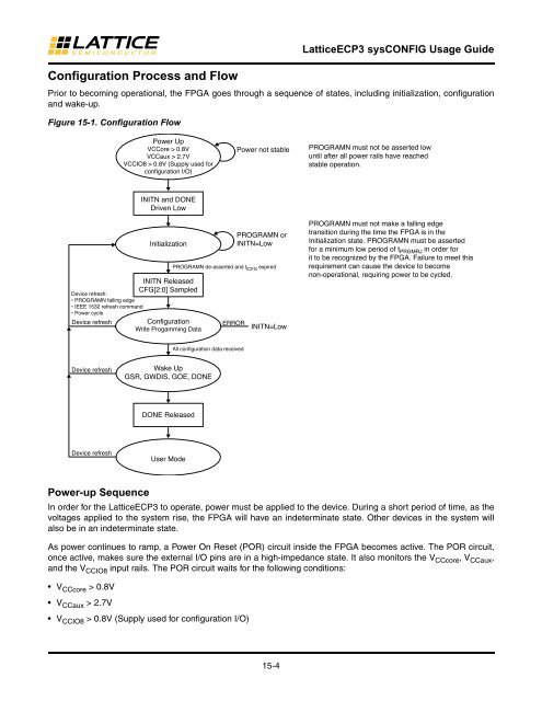
Configuration Process and Flow<br />
15-4<br />
<strong><strong>Lattice</strong>ECP3</strong> <strong>sysCONFIG</strong> <strong>Usage</strong> <strong>Guide</strong><br />
Prior to becoming operational, the FPGA goes through a sequence of states, including initialization, configuration<br />
and wake-up.<br />
Figure 15-1. Configuration Flow<br />
Power-up Sequence<br />
Power Up<br />
VCCore > 0.8V<br />
VCCaux > 2.7V<br />
VCCIO8 > 0.8V (Supply used for<br />
configuration I/O)<br />
INITN and DONE<br />
Driven Low<br />
Initialization<br />
INITN Released<br />
CFG[2:0] Sampled<br />
Device refresh:<br />
• PROGRAMN falling edge<br />
• IEEE 1532 refresh command<br />
• Power cycle<br />
Device refresh<br />
Configuration<br />
Write Progamming Data<br />
Device refresh<br />
Device refresh<br />
Wake Up<br />
GSR, GWDIS, GOE, DONE<br />
DONE Released<br />
User Mode<br />
ERROR<br />
In order for the <strong><strong>Lattice</strong>ECP3</strong> to operate, power must be applied to the device. During a short period of time, as the<br />
voltages applied to the system rise, the FPGA will have an indeterminate state. Other devices in the system will<br />
also be in an indeterminate state.<br />
As power continues to ramp, a Power On Reset (POR) circuit inside the FPGA becomes active. The POR circuit,<br />
once active, makes sure the external I/O pins are in a high-impedance state. It also monitors the V CCcore , V CCaux ,<br />
and the V CCIO8 input rails. The POR circuit waits for the following conditions:<br />
VCCcore > 0.8V<br />
VCCaux > 2.7V<br />
VCCIO8 > 0.8V (Supply used for configuration I/O)<br />
Power not stable<br />
PROGRAMN or<br />
INITN=Low<br />
PROGRAMN de-asserted and t ICFG expired<br />
All configuration data received<br />
INITN=Low<br />
PROGRAMN must not be asserted low<br />
until after all power rails have reached<br />
stable operation.<br />
PROGRAMN must not make a falling edge<br />
transition during the time the FPGA is in the<br />
Initialization state. PROGRAMN must be asserted<br />
for a minimum low period of t PRGMRJ in order for<br />
it to be recognized by the FPGA. Failure to meet this<br />
requirement can cause the device to become<br />
non-operational, requiring power to be cycled.