計畫詳細資料 - NSRRC User Portal
計畫詳細資料 - NSRRC User Portal
計畫詳細資料 - NSRRC User Portal

Create successful ePaper yourself
Turn your PDF publications into a flip-book with our unique Google optimized e-Paper software.
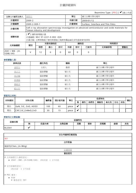
<strong>計畫詳細資料</strong><br />
Beamtime Type: [PEC] [ ]線上申請<br />
主持人/協同主持人 馮哲川 單位 國立台灣大學光電所<br />
計畫期別 2009-2 申請日期 2009/01/12<br />
計畫編號 2009-2-009-1 計畫領域 Surface, Interface and Thin Films<br />
計畫名稱<br />
經費來源<br />
光束線編號 類別<br />
20A1 / BM - (H-<br />
SGM) XAS<br />
參與實驗人員:<br />
將使用之材料:<br />
Soft x-ray absorption spectroscopy investigation on advanced semiconductor and oxide materials for<br />
Taiwan industry and development<br />
[ ] 國科會專題計畫<br />
計畫編號: NSC 97-2221-E-002 -026<br />
計畫名稱: 功率與微電子應用與發展之塊狀與磊晶碳化矽的創新研究(III)<br />
本期申請時段 總時段 特殊需求<br />
理想 最小 核可 申請 核可 已使用 光束線排程 實驗站<br />
V 12 6 0 60 0 0<br />
參與成員 擔任角色 職稱 單位<br />
馮哲川 主持人 教授 國立台灣大學光電所<br />
吳于立 協助實驗 碩士生 國立台灣大學光電所<br />
吳宗翰 協助實驗 碩士生 國立台灣大學光電所<br />
林澤暘 協助實驗 碩士生 國立台灣大學光電所<br />
楊喻丞 協助實驗 碩士生 國立台灣大學光電所<br />
藍右任 協助實驗 碩士生 國立台灣大學光電所<br />
材料類別 材料名稱 攜帶量 預計使用量 單位<br />
樣品 GaN, SiC, ZnO, Al2O3 100 60 piece<br />
樣品 CNT,SiC,ZnMnO,ZnO 30 15 piece<br />
將使用之主要設備:<br />
BL20A1<br />
無!!<br />
設備名稱<br />
陳錦明(Chen, Jin-Ming)<br />
# 光束線發言人審核意見:<br />
危害特性<br />
無 毒性 易燃性 腐蝕性 氧化性 生化 其他<br />
無 低溫冷凍 加熱設備<br />
設備特性<br />
高壓 雷射 高電壓 鈹窗 其他<br />
� 20A1 - BM - (H-SGM) XAS: (X)同意 ( )不同意<br />
# 安全組審核意見:<br />
(X)同意 ( )不同意<br />
# PEC 審查:<br />
� VUV<br />
# 審查意見: 無!!<br />
安全考慮與防範措施<br />
合作對象<br />
計畫背景<br />
審查意見<br />
備註
A proposal to <strong>NSRRC</strong>:<br />
Soft X-Ray Absorption Spectroscopy Investigation on Advanced Semiconductor<br />
and Oxide Materials for Taiwan Industry and Development (Beamline: BL20A)<br />
{from 馮哲川教授,國立台灣大學光電所,台北市 106 羅斯福路四段一號<br />
Prof. Zhe Chuan Feng, Graduate Institute of Photonics & Optoelectronics and Department of<br />
Electrical Engineering, National Taiwan University, Taipei, 106-17 Taiwan, ROC<br />
Office: Barry Lam Hall-417 (博理館 417 室); Tel: 886-2-3366-3543, Fax: 886-2-2367-7467<br />
E-mail: fengzc@cc.ee.ntu.edu.tw; zhechuan_feng@yahoo.com;<br />
Web: http://gipo.ntu.edu.tw/; http://www.ee.ntu.edu.tw/}<br />
(A) Background<br />
The principal investigator (P.I.), Z. C. Feng (馮哲川), and students at National Taiwan<br />
University (NTU) had previously performed a proposal research with <strong>NSRRC</strong>, “Soft X-Ray<br />
Near-Edge Absorption Fine Structure Spectroscopy Investigation on Semiconductor Materials”,<br />
using Beamline of BL20A. Within the first exploration beam times of 8.3 shifts in 2008 July<br />
29-August 1, we have obtained some useful data on ZnMnO, GaN/Si and related materials.<br />
A1. Our preliminary data using BL20A<br />
Soft X-Ray Absorption Spectroscopy (SXAS) data using BL20A have been obtained and<br />
typical data near oxygen (O) K-edge and Zn L-edge are shown below.<br />
Intensity<br />
10000<br />
5000<br />
file: Zo-undoped<br />
XAS Intensity<br />
25000<br />
20000<br />
15000<br />
10000<br />
5000<br />
O K-edge<br />
ZnO bulk, undoped<br />
520 530 540 550 560 570<br />
O K-edge<br />
Energy (eV)<br />
ZnO:Co-doped<br />
bulk<br />
520 530 540 550 560 570<br />
Energy (eV)<br />
file: Zo-Co<br />
Intensity<br />
Intensity<br />
1<br />
30000 O K-edge<br />
25000<br />
20000<br />
15000<br />
10000<br />
file:Zo-Ho<br />
20000<br />
15000<br />
10000<br />
5000<br />
ZnO:Ho-doped, bulk<br />
520 530 540 550 560 570<br />
Energy (eV)<br />
25000 O K-edge<br />
file: Zo-Ga<br />
ZnO:Ga-doped, bulk<br />
520 530 540 550 560 570<br />
Energy (eV)
Intensity<br />
XAS Intensity<br />
Intensity<br />
40000<br />
30000<br />
20000<br />
10000<br />
file: Z130Sap<br />
Intensity<br />
20000<br />
15000<br />
10000<br />
5000<br />
O K-edge<br />
ZnO on sapphire (Al O ) 2 3<br />
MOCVD<br />
520 530 540 550 560 570<br />
O K-edge<br />
Energy (eV)<br />
520 530 540 550 560 570<br />
Energy (eV)<br />
Zn L-edge:<br />
100000 Zn L-edge<br />
80000<br />
60000<br />
40000<br />
20000<br />
60000<br />
40000<br />
20000<br />
ZnO:Cu on Si<br />
PECVD<br />
ZnO+Cu(1) 2Pa T-R 30min (A-1)<br />
1000 1010 1020 1030 1040 1050<br />
Energy (eV)<br />
Zn L-edge<br />
ZnO:Cu on Si<br />
PECVD<br />
A-1,ZnO+Cu(1) 2Pa 205u 600C T-R 25min<br />
ZnO on Sapphire<br />
MOCVD<br />
1000 1010 1020 1030 1040 1050<br />
file: Z130Sap<br />
Energy (eV)<br />
Intensity<br />
Intensity<br />
2<br />
30000 O K-edge<br />
25000<br />
20000<br />
15000<br />
10000<br />
5000<br />
file: Z130Si<br />
Intensity<br />
Intensity<br />
20000<br />
15000<br />
10000<br />
5000<br />
file: Hf01d<br />
100000<br />
50000<br />
60000<br />
40000<br />
20000<br />
0<br />
ZnO on Si<br />
MOCVD<br />
520 530 540 550 560 570<br />
Energy (eV)<br />
O K-edge<br />
Nano-scale<br />
HfO2 layer on Si<br />
520 530 540 550 560 570<br />
Zn L-edge<br />
Energy (eV)<br />
ZnO:Co-doped<br />
bulk<br />
0<br />
1000 1010 1020 1030 1040 1050<br />
Energy (eV)<br />
file: Zo-Co<br />
Zn L-edge<br />
ZnO on Si<br />
MOCVD<br />
1000 1010 1020 1030 1040 1050<br />
Energy (eV)<br />
file: Z130Si
Intensity<br />
100000<br />
80000<br />
60000<br />
40000<br />
20000<br />
Zn L-edge<br />
ZnO:Ho-doped<br />
bulk<br />
0<br />
1000 1010 1020 1030 1040 1050<br />
Energy (eV)<br />
file: Zo-Ho<br />
Intensity<br />
3<br />
120000<br />
100000<br />
80000<br />
60000<br />
40000<br />
20000<br />
Zn L-edge<br />
ZnO :Mg:Li<br />
co-doped bulk<br />
0<br />
1000 1010 1020 1030 1040 1050<br />
Energy (eV)<br />
file: Zo-MLb<br />
The BL20A HSGM Beamline covers energy range of 60-1250 eV. It is suitable to perform<br />
Soft X-Ray Absorption Spectroscopy (SXAS) measurements on not only above O K-edge (537 eV),<br />
Zn L-edge (1020, 1043 and 1194 eV), but also C K-edge (284 eV) and N K-edge (402 eV). These<br />
would be very useful for our research on wide gap semiconductors GaN, ZnO, SiC and oxides as<br />
well as alloys/structure. Students are going on studying the program fitting and simulations on<br />
above and future data. But our students may need to get more help and training from BL20A<br />
experts on program fitting and simulations.<br />
A2. Some useful reference works from literature<br />
Fig. 1 displays C K-edge XANES spectra of N-CNTs with and without chlorine treatment and<br />
the highly oriented pyrolytic graphite (HOPG) as a reference. The feature with the maximum<br />
intensity at approximately 285.5 eV for HOPG was attributed to the π* antibonding state<br />
originated from the out-of-plane bonds in the sp 2 bonding configuration. The positions of π*<br />
resonance feature in the C (1s) XANES spectra of N-CNTs and N-CNTs: Cl located at ~286.4 and<br />
286.7 eV, respectively, which are shifted by ~0.9 eV for N-CNTs and 1.2 eV for N-CNTs: Cl with<br />
respect to that of HOPG (285.5 eV), correspond to the 1s→π*(e2u) transition as in the pyridinelike<br />
sp 2 C–N structure. Fig. 2 displays the N K-edge XANES spectra of the N-CNTs and N-CNTs: Cl<br />
samples. The two main features centered at ~403.2 and ~409.5 eV are associated with transitions<br />
into unoccupied π* and σ* orbitals, respectively [1].<br />
Fig. 3 shows the absorption spectra of all three investigated samples after normalization to the<br />
same edge height: cubic GaN (a), nitrided GaAs (b), and hexagonal GaN (c). The angle of incidence<br />
was chosen to be 38°. At this angle close to the so-called ‘‘magic angle’’ the spectra are directly<br />
comparable because for surfaces with at least threefold symmetry the spectra are independent of the<br />
orbital orientation. Fig. 4 shows the dependence of the absorption spectra on the angle of incidence<br />
and thus on the direction of the polarization vector with respect to the sample surface. The aim of<br />
these measurements is to determine the orientation of the a-GaN crystallites. The arrows in the<br />
figure indicate the development of the intensities for increasing θ [2].
FIG. 1. C K-edge XANES spectra of FIG. 2. N K-edge XANES spectra of<br />
unchlorinated/chlorinated N-CNTs and unchlorinated/chlorinated N-CNTs.<br />
reference HOPG. The inset highlights The inset highlights the π* region [1].<br />
the π* region [1].<br />
FIG. 3. X-ray absorption spectra of hexagonal FIG. 4. Polarization dependent x-ray absorption<br />
GaN (a), nitrided GaAs (001) (b), and cubic GaN (c). spectra of hexagonal GaN for angles of incidence<br />
The angle of incidence was 38°, which is close to Θ between 0° and 64°. The geometry is sketched<br />
the magic angle. Absorption features are marked in the upper right comer. The development of the<br />
by vertical bars and labeled P1–P8. The bottom intensities for increasing off normal angles is<br />
curve (d) represents the difference between given by the arrows [2].<br />
spectrum (b) and a weighted average of the<br />
spectra (a) and (b) with weighting factors of<br />
0.2 and 0.8, respectively [2].<br />
4
The TEY XANES spectra measured at different incident angles were shown in Fig. 5. The<br />
sharp excitons at 285.4 and 291.5 eV are attributed to the dipolar transition of core level 1s electron<br />
into the C–C π* and C–C σ* states in the conduction band, respectively. Two other σ*<br />
transitions from 292 to 298 eV and broad (π+σ) transitions from 301 to 309 eV are also observed.<br />
Two small peaks in 287–290 eV can be assigned to the oxygenated surface functionalities perhaps<br />
associated with the defects of the nanotubes. The angular dependence of the π* and σ* excitations<br />
can be understood by studying the electronic structure [3].<br />
FIG. 5. Angle-resolved TEY XANES spectra of SWNT forest grown on silicon wafer. The inset shows the<br />
incident geometry of π* vector orbitals and σ* planes for a vertical SWNT tube axis (along z) on Si wafer<br />
with respect to the incident beam and the electric field vector E which remains perpendicular to the incident<br />
x-ray beam [3].<br />
The annealing-temperature dependence in valence-band photoemission spectra and O K -edge<br />
absorption spectra for poly- Si/HfO2 /Si and HfO2 /Si are shown in Fig. 6 and Fig. 7 respectively.<br />
Broad structures from EF to 4 eV and from 4 to 10 eV are derived from Si and O 2p components,<br />
respectively. By the annealing at 700 °C, the intensity of SiO2 is increased due to the SiO2<br />
formation at the upper interface. On the other hand, the decrease in the SiO2 component by 750 °C<br />
annealing is related to the SiO2 consumption by the chemical reaction. Without the poly-Si layer,<br />
the crystallization temperature of the HfO2 layer is not changed as shown in Fig. 7. It suggests that<br />
the poly-Si layer does not affect the crystallization temperature of HfO2 [4].<br />
5
FIG. 6. Annealing-temperature dependence of FIG. 7. Annealing-temperature dependence of<br />
poly-Si/HfO2 /Si structures in (a) valence-band HfO2 /Si structures in (a) valence-band<br />
photoemission spectra and (b) O K-edge absorption photoemission spectra and (b) O K-edge<br />
spectra. Double peaks in XAS are assigned as HfO2 absorption spectra. Peak in XAS are assigned<br />
and SiO2 [4]. as HfO2 and SiO2 [4].<br />
FIG. 8 Normalized O K-edge XANES spectra of Zn1−xCoxO<br />
and Zn1−xMgxO nanorods. The upper inset shows magnified<br />
view of A1 and B1 features of the Zn1−xCoxO and Zn1−xMgxO<br />
nanorods. The lower inset presents normalized Zn L3-edge<br />
spectra of Zn1−xCoxO and Zn1−xMgxO nanorods [5].<br />
Fig. 8 presents normalized O K-edge XANES<br />
spectra of Zn1−xCoxO and Zn1−xMgxO nanorods.<br />
Features A1–E1 of Zn1−xCoxO and Zn1−xMgxO are<br />
attributable to electron transition from O 1s to<br />
2pσ(along the bilayer) and O 2pπ(along the c axis)<br />
states. The fact that the intensities of these features are<br />
lower than those of ZnO (clearly seen in the upper inset)<br />
shows that the number of unoccupied O 2p-derived<br />
states is reduced, which can be interpreted as transfer of<br />
electrons from Co and Mg dopants to O 2p states due to<br />
6
O 2p–Co 3d and O 2p–Mg 3sp hybridizations in Zn1−xCoxO and Zn1−xMgxO nanorods, respectively.<br />
Fig. 9(a) presents normalized Mg K-edge XANES spectra of Zn1−xMgxO nanorods, MgO, and Mg<br />
metal. Spectral line shapes of the Mg metal clearly differ from those of the Zn1−xMgxO and MgO<br />
samples hybridization. Fig. 9(b) presents normalized Co L3,2-edge XANES spectra of Zn1−xCoxO<br />
nanorods, CoO, and Co metal, for transition of electrons from Co 2p3/2 (L3) and 2p1/2 (L2) states<br />
to unoccupied Co 3d and 4s states. The general line shapes of the Co L3,2-edge XANES spectra of<br />
the Zn1−xCoxO nanorods are similar to those of polycrystalline Zn1−xCoxO bulk/film [5].<br />
FIG. 9. (a) Normalized Mg K-edge XANES spectra of Zn1−xMgxO nanorods, MgO, and Mg metal. (b) shows<br />
Co L3,2-edge spectra of Zn1−xCoxO nanorods, CoO, and Co metal [5].<br />
A3. Attractive works of soft XAS reported in 2008 from literature<br />
FIG. 10. Several soft XAS spectra of Sr2FeMoO6<br />
with additional total fluorescence yield (TFY).<br />
Multiplet calculations for different Fe 2+ and Fe 3+<br />
ratios are also shown in red lines [6].<br />
7<br />
Fig. 11. A series of C Kα RXES spectra from CDO<br />
acquired at 298 eV, 289 eV, 287 eV, 286 eV and<br />
280.5 eV for (i) to (v) respectively [7].
Quite recently, several attractive papers, using synchrotron radiation soft X-ray absorption<br />
emission spectroscopy technology, have been just published in 2008, “Fe valence state of<br />
Sr2FeMoO6 probed by x-ray absorption spectroscopy: The sample age matters” [6], “Electronic<br />
structure characterization of ultra low-k carbon doped oxide using soft X-ray emission<br />
spectroscopy” [7], “Transition layers at the SiO2 /SiC interface” [8], “Control of oxidation and<br />
reduction reactions at HfSiO/Si interfaces through N exposure or incorporation” [9] and “Charge<br />
transfer across the molecule/metal interface using the core hole clock” [10].<br />
Figure 10 shows several soft XAS spectra taken for Sr2FeMoO6 with additional total<br />
fluorescence yield (TFY) spectra recorded. Multiplet calculations for different Fe 2+ and Fe 3+ ratios<br />
are also shown in red lines [6]. Fig. 11 gives a series of C Kα RXES spectra from CDO acquired at<br />
298 eV, 289 eV, 287 eV, 286 eV and 280.5 eV for (i) to (v) respectively [7]. CDO (Carbon doped<br />
oxide) is a ultra low-k (ULK) material with its k value less than 2.5, which is a good candidate for<br />
new generation semiconductor IC application for dimension less than 50nm.<br />
Fig. 11 shows (a) Z-contrast STEM image, (b) Si-L2,3 edge (99 eV) and (c) C-K edge (284 eV)<br />
from the SiO2 /4H-SiC interface [8]. Fig. 12 shows photoemission spectra of (a) Hf 4f and (b) Si 2p<br />
from the HfSiON film with the N2 partial pressure (PN2) dependence [9].<br />
Fig. 11 (a) Z-contrast STEM image, (b) Si-L2,3<br />
edge (99 eV) and (c) C-K edge (284 eV) of the SiO2<br />
/4H-SiC interface [8].<br />
8<br />
Fig. 12. (a) Hf 4f and (b) Si 2p photoemission<br />
spectra of the HfSiON film with the N2 partial<br />
pressure (PN2) dependence [9].
P.I.’s long term collaborator, Prof. Andrew Thye Shen Wee (National University of Singapore)<br />
and collaborators, have recently publish a good long review report “Charge transfer across the<br />
molecule/metal interface using the core hole clock”, at Surface Science Reports [10]. Fig. 13 shows<br />
Core-hole clock spectra for (a) a conjugated polymer of poly(para-phenylenevinylene) and (b)<br />
BFF-SAM on Au(111) across the N k-edge absorption threshold [10]. Fig. 14 shows (a)<br />
Synchrotron-based high-resolution C 1s core level PES spectrum of BFF-SAM on au(111)<br />
measured with photon energy of 350 eV, and (b) corresponding C k-edge NEXAFS spectrum. The<br />
right panel in Fig. 14 presents the detailed molecular structure of BFF-SAM with different carbon<br />
species [10].<br />
Fig. 13. Core-hole clock spectra for (a) a<br />
conjugated polymer of poly(para-phenylenevinylene)<br />
and (b) BFF-SAM on Au(111) across the N k-edge<br />
absorption threshold [10].<br />
9<br />
Fig. 14. (a) Synchrotron-based high-resolution C<br />
1s core level PES spectrum of BFF-SAM on Au(111)<br />
measured with photon energy of 350 eV, and (b)<br />
corresponding C k-edge NEXAFS spectrum. The<br />
right panel shows the detailed molecular structure<br />
of BFF-SAM with different carbon species [10].<br />
A4. Some useful related works from other research groups in Taiwan<br />
Prof. J. M. Chen, collaborators and others had performed a series of X-Ray Absorption<br />
Spectroscopy (XAS) studies for superconductors and other materials. Two plots below showed the<br />
Co L2,3-edge and O K-edge XNEAS and fits for superconductor [(Bi,Pb2Ba2O4±ω)]0.5CoO2 [11].<br />
Soft-XAS using BL20A with Mn-L2,3 and (b) Sn-M3 for LSnMO film was studied [12].
Ref. [12]: FIG. 3. The x-ray absorption spectra of (a) Mn-L2,3 and (b) Sn-M3 for LSnMO film, respectively.<br />
Spectra for various standard reference compounds are also displayed for comparison.<br />
Below show the Cu L3,2-edge for LiCu2O2 [13] and Fe L3,2-edge for Sr2FeMo1−xNbxO6 [14] soft<br />
X-ray absorption near edge spectra. In particular, ref. [14] is published in 2009 just a few days ago<br />
as P.I. prepare this proposal.<br />
10
(B) significance, objective, and expected outcome of the proposal<br />
1. Significance<br />
Research and development on wide energy gap semiconductors and structures for<br />
optoelectronic and electronic applications have been very active in recent years [15-20]. III-nitride<br />
semiconductors possess large direct band gaps, extremely high hardness, very large heterojunction<br />
offsets, high thermal conductivity and high melting temperature. Great breakthroughs have been<br />
achieved in recent years for their materials growth and device manufactures in applications in<br />
blue-UV light emitting diode (LED), laser diode (LD) and other optoelectronic and electronic<br />
devices. Taiwan industry for III-Nitride and III-V based LEDs have occupied an important position<br />
in the world range, which has provided most of materials studied in this proposal. We hope to serve<br />
for the further development of Taiwan industry in this field through our penetrating research<br />
including by help of powerful synchrotron radiation facilities.<br />
High energy and high intensity synchrotron radiation technology can be a powerful tool for<br />
materials fundamental research. It is worthy to perform more wide and extended investigation on<br />
those wide gap semiconductors, GaN, AlN, ZnO, SiC and oxides. To our previous experiences<br />
(even not very many) Soft X-ray Near-Edge Absorption Fine Structure Spectroscopy can play an<br />
11
important rule to promote research in this filed. A part of evidences have been presented in the<br />
section (A).<br />
2. Objective<br />
We plan to use <strong>NSRRC</strong> Soft X-ray Absorption Spectroscopy end station at BL20A to perform<br />
SR XAS and XES investigations on wide range of nano-structural materials and samples. Each<br />
material will include samples of undoped, n-type and p-type doped with different doping levels,<br />
varied compositions or growth conditions. These SR XAS and XES studies will be combined with<br />
many other optical, structural and other materials analytical measurements to reach comprehensive<br />
and penetrating understanding and control of materials properties.<br />
3. Research distinguishing feature<br />
The distinguishing features of the proposed research include: to get great potential in future<br />
spintronics applications on ZnMnO and related materials, to use the most advantages of synchrotron<br />
radiation technology which are unable to realize by ordinary XPS techniques. Using soft X-ray<br />
absorption spectroscopy (XAS) and X-ray emission spectroscopy (XES), we can obtained in depth<br />
the knowledge and information about the electronic structures and states, electronic properties of<br />
the surface and interface, chemical bonding states, oxidation states and Fermi level pinning on<br />
ZnMnO, wide gap semiconductors, GaN, InN, AlN, InGaN, AlGaN, AlInGaN, SiC, ZnO, ZnMgO<br />
and oxides of HfO2, Al2O3, Ga2O3, Si3N4, as well as related materials.<br />
4. Expected Outcome<br />
We’ve gotten all Near-edge X-ray absorption fine structure spectroscopy (NEXAFS) data for<br />
planed materials. Data analyses and processing will be performed. The corresponding information<br />
on the electronic structures and states, electronic properties of the surface and interface, chemical<br />
bonding states, crystallite size, strain analysis and extended defects can be obtained. Their effects<br />
from doping, composition and growth conditions should be gained, in combination with other<br />
results from optical and structural measurements on these samples. These provide in-depth<br />
knowledge on these advanced nano-semiconductors which are very useful to the R&D on these new<br />
generation materials. We should get 2-3 good papers for high SCI level journals or important<br />
international academic conferences per year. The work will lay a good foundation for further<br />
extensive R&D on other materials using synchrotron radiation technology.<br />
(C) Why Synchrotron Radiation is Needed<br />
The principal investigator (P.I.), Z. C. Feng (馮哲川), and collaborators including students<br />
have devoted in the research and exploration on various semiconductors and structures. We have<br />
performed multiple optical and structural investigations on different semiconductors with high<br />
values of outputs, for example, within only recent 3-years of 2006-2008, produced 25 SCI journal<br />
12
papers, selectively listed as [21-26]. However, the ordinary optical and structural techniques are<br />
limited in the exploration of materials properties in depth, which hindered the investigation in depth<br />
on these materials. The experimental techniques of synchrotron radiation high energy XPS and<br />
SR-XRD have been employed by us for further studies on semiconductor materials with significant<br />
results [27-29]. Near-Edge X-ray Absorption Fine Structure Spectroscopy (NEXAFS) using<br />
<strong>NSRRC</strong> beamline 17C for CdSeTe and CdZnTe alloys and MOCVD grown GaN on Si have been<br />
recently leaded to a series of significant conference papers and reports [30-32], which will be soon<br />
further going to make for high level journal papers. Also, <strong>NSRRC</strong> BL16A has been shown very<br />
suitable for our wide gap semiconductor SiC materials for the Si K-edge NEXAFS measurements<br />
[33]. High energy NEXAFS using BL17C with photon energy between 4-15 keV is suitable for<br />
K-edges of Ga, Zn, Se, Ge, Mn, Fe, Cu etc. The BL20A with photon energy in 60-1250 eV is<br />
powerful for soft x-ray near-edge absorption fine structure spectroscopy measurements on K-edges<br />
of elements O, N, C, and L-edges of Zn and lighter elements, which have been approved by our<br />
preliminary practice, listed in section A1, and others researches (A2, A3 and A4). So, we would have<br />
<strong>NSRRC</strong> above three powerful beamlines for entire energy spectral range of our wide gap<br />
semiconductors and oxides.<br />
Soft x-ray near-edge absorption fine structure spectroscopy on semiconductors and related<br />
materials can determine clearly their bulk electronic structure, electronic properties of the surface,<br />
near edge x-ray absorption fine structure, electronic states in valence and conduction bands with<br />
high energy resolution and advantage of the linear polarization of the synchrotron radiation and<br />
careful crystallographic orientation of the samples, to reveal the concentration of oxidation states, to<br />
identify the chemical bonding states of the buried silicon carbide layers and hydrogen-terminated<br />
surfaces as well as the Fermi level pinning. These are very significant to understand these advanced<br />
semiconductor materials. Near-edge X-ray absorption fine structure spectroscopy (NEXAFS) is a<br />
particularly useful and effective technique for simultaneously probing the surface chemistry, surface<br />
molecular orientation, degree of order, and electronic structure of III-Nitride, SiC- and ZnO-based,<br />
various oxides and other materials which are extremely needed for our research.<br />
(D) An estimate of the number of shifts required and the reason for using the beamline<br />
We propose to use the beamline BL20A for K-edge XAS measurements on elements N, C and<br />
O, and L-edge XAS for Zn, Mn, Co, Al, Mg, from our various advanced materials of GaN, InN,<br />
AlN, SiN, CNTs, SiC (3C-, 4H- and 6H-polytypes), nano-HfO2 and Al2O3 on Si, ZnO, ZnMgO,<br />
ZnMnO, ZnCoO, Ga2O3/GaAs and related materials. We propose to make a 2-years plan for a total<br />
of 36-shifts, with 6-shifts per 4-months. We can adjust, increase or decrease the use of shifts per<br />
4-months. After measurements, we perform data processing and theoretical analyses. And this study<br />
is useful to further deepen our understanding for the physical and chemical properties of these wide<br />
energy gap semiconductors and oxides.<br />
13
(E) List of publications relevant to <strong>NSRRC</strong> beamlines during the preceding year<br />
1. Publications (cited in above text)<br />
[1] S. C. Ray, C. W. Pao and H. M. Tsai ed. “Electronic structures and bonding properties of chlorine-treated<br />
nitrogenated carbon nanotubes: X-ray absorption and scanning photoelectron microscopy studies” Appl.<br />
Phys. Lett. 90, 192107 (2007).<br />
[2] M. Lubbe, P.R. Bressler and W. Braun ed. “Near edge x-ray absorption fine structure characterization of<br />
polycrystalline GaN grown by nitridation of GaAs (001)” J. Appl. Phys. 86, 209 (1999).<br />
[3] Zhongrui Li, Liang Zhang and Daniel E. Resasco ed.”Angle-resolved x-ray absorption near edge<br />
structure study of vertically aligned single-walled carbon nanotubes” Appl. Phys. Lett. 90, 103115<br />
(2007).<br />
[4] H. Takahashi, J. Okabayashi and S. Toyoda ed. ”Mechanism of Hf-silicide formation at interface<br />
between poly-Si electrode and HfO2 /Si gate stacks studied by photoemission and x-ray absorption<br />
spectroscopy” J. Appl. Phys. 99, 113710 (2006).<br />
[5] J. W. Chiou, H. M. Tsai and C. W. Pao ed. ”Comparison of the electronic structure of Zn1-xCoxO and<br />
Zn1-xMgxO nanorods using x-ray absorption and scanning photoelectron microscopies” Appl. Phys. Lett.<br />
89, 043121 (2006).<br />
[6] K. Kuepper, M. Raekers, C. Taubitz, H. Hesse, M. Neumann, A. T. Young, C. Piamonteze, F. Bondino,<br />
and K. C. Prince, “Fe valence state of Sr2FeMoO6 probed by x-ray absorption spectroscopy: The sample<br />
age matters”, J. Appl. Phys. 104, 036103 (2008).<br />
[7] I. Reid, Y. Zhang, A. DeMasi, G. Hughes, K.E. Smith, “Electronic structure characterization of ultra<br />
low-k carbon doped oxide using soft X-ray emission spectroscopy”, Thin Solid Films 516, 4851 (2008).<br />
[8] Tsvetanka Zheleva, Aivars Lelis, Gerd Duscher, Fude Liu, Igor Levin, and Mrinal Das, “Transition layers<br />
at the SiO2 /SiC interface”, Appl. Phys. Lett. 93, 022108 (2008).<br />
[9] H. Kamada, T. Tanimura, S. Toyoda, H. Kumigashira, M. Oshima, G. L. Liu, Z. Liu, and K. Ikeda,<br />
“Control of oxidation and reduction reactions at HfSiO/Si interfaces through N exposure or<br />
incorporation”, Appl. Phys. Lett. 93, 212903 (2008).<br />
[10] Li Wang, Wei Chen, Andrew Thye Shen Wee, “Charge transfer across the molecule/metal interface<br />
using the core hole clock”, Surface Science Reports 63, 465–486 (2008).<br />
[11] K. Sakai, M. Karppinen, J. M. Chen, R. S. Liu, S. Sugihara and H. Yamauchi, “Pb-for-Bi substitution<br />
for enhancing thermoelectric characteristics of [(Bi,Pb2Ba2O4±ω)]0.5CoO2”, Appl. Phys. Lett. 88,<br />
232102 (2006).<br />
[12] T. Y. Cheng, C. W. Lin, L. Chang, C. H. Hsu, J. M. Lee, J. M. Chen, J.-Y. Lin, K. H. Wu, T. M. Uen, Y.<br />
S. Gou, and J. Y. Juang, “Magnetotransport properties, electronic structure, and microstructure of<br />
La0.7Sn0.3MnO3 thin films”, Phys. Rev. B 74, 134428 (2006).<br />
[13] C. L. Chen, K. W. Yeh, D. J. Huang, F. C. Hsu, Y. C. Lee, S. W. Huang, G. Y. Guo, H.-J. Lin, S. M.<br />
Rao, and M. K. Wu, “Orbital polarization of the unoccupied states in multiferroic LiCu2O2”, Phys. Rev.<br />
B 78, 214105 (2008).<br />
[14] B.-G. Park, Y.-H. Jeong, and J.-H. Park, J. H. Song, J.-Y. Kim, H.-J. Noh, H.-J. Lin and C. T. Chen,<br />
“Physical properties and electronic evolution of Sr2FeMo1−xNbxO6 (0
[23] K. Y. Lo, Y. J. Huang, J. Y. Huang, Z. C. Feng, W. E. Fenwick, M. Pan and I. T. Ferguson, “Reflective<br />
Second Harmonic Generation from ZnO thin films: A study on the Zn-O bonding”, Appl. Phys. Lett. 90,<br />
161904 (2007).<br />
[24] S. J. Wang, Nola Li, E. H. Park, Z. C. Feng, A. Valencia, J. Nause and I. T. Ferguson, “Metalorganic<br />
Chemical Vapor Deposition of InGaN Layers on ZnO Substrates”, J. Appl. Phys. 102, 106105 (2007).<br />
[25] Z. C. Feng, S. C. Lien, J. H. Zhao, X. W. Sun and W. Lu, “Structural and Optical Studies on<br />
Ion-implanted 6H-SiC Thin Films”, Thin Solid Films, 516, no.16, 5217-5226 (2008).<br />
[26] S. Sun, G. S. Tompa, C. Rice, X. W. Sun, Z. S. Lee, S. C. Lien, C. W. Huang, L. C. Cheng and Z. C.<br />
Feng, “Metal organic chemical vapor deposition and investigation of ZnO thin films grown on sapphire”,<br />
Thin Solid Films, 516, no.16, 5572-5277 (2008).<br />
[27] Z.C. Feng, L.C. Cheng, C.W. Huang and Y.L. Wang, “Synchrotron Radiation X-ray Photoelectron<br />
Spectroscopy and X-ray Diffraction Investigation on Si-based Structures for Sub-micron Si-IC<br />
Applications”, TAIWAN-INDIA CONFERENCE ON NANOMATERIALS, Taoyuan, Taiwan, OS-07,<br />
9-pages (2006).<br />
[28] L. C. Cheng, F. C. Hou, Z. C. Feng, C. C. Tin, C. H. Kuan, Y. W. Yang, “Raman Scattering and X-ray<br />
Photoelectron Spectroscopy Studies of Cubic Silicon Carbide grown on Si(100) by Chemical Vapor<br />
Deposition”, International Workshop on Widegap Semiconductors (IWWWS) 2007, 6-pages, CD-1.<br />
[29] S. Sun, G. S. Tompa, C. Rice, X. W. Sun, Z. S. Lee, S. C. Lien, C. W. Huang, L. C. Cheng and Z. C.<br />
Feng, “Metal organic chemical vapor deposition and investigation of ZnO thin films grown on sapphire”,<br />
Thin Solid Films, 516, no.16, 5572-5277 (2008).<br />
[30] Yen-Ting Chen, Zhe Chuan Feng, Jyh-Fu Lee, Ian Ferguson, and Weijie Lu, “X-ray Absorption<br />
Fine-structure Spectroscopy Investigation on CdSeTe Alloys for Photovoltaic Application”, International<br />
Electron Devises and Materials Symposia (IEDMS) 2008, 4-pages, CD-496.<br />
[31] Yi-Li Tu, Yen-Ting Chen, Zhe Chuan Feng, N.C. Chen, Jyh-Fu Lee, “X-ray Absorption Fine-Structure<br />
Spectroscopy Investigation of GaN Thin Films on Si”, International Conference on Optics and Photonics<br />
in Taiwan (OPT) 2008, Taipei, 4-pages, CD Sat-S32-02.<br />
[32] Yen-Ting Chen, Yu Li Wu, Zhe Chuan Feng, Jyh-Fu Lee, and Weijie Lu, “X-ray Absorption<br />
Fine-structure Spectroscopy on CdZnTe Ternary Alloys”, International Conference on Optics and<br />
Photonics in Taiwan (OPT) 2008 & International Symposium on Solar Cell Technology (ISSCT) 2008,<br />
Taipei, 4-pages, CD Sat-S26-02.<br />
[33] Yi-Li Yu, Tse-Yang Lin, Zhe Chuan Feng, Ling-Yun Jang, and Weijie Lu, “Synchrotron Radiation<br />
X-Ray Absorption Spectroscopy Investigation on Bulk SiC Materials”, <strong>NSRRC</strong> 2008 user meeting and<br />
symposia.<br />
2. abstract title for <strong>NSRRC</strong> users' meeting<br />
Synchrotron radiation Soft X-ray absorption spectroscopy investigation on advanced<br />
semiconductors and oxides for Taiwan industry application.<br />
2. abstract title for<br />
Soft X-ray absorption spectroscopy studies on advanced semiconductors and oxides for LED<br />
industry application by help of synchrotron radiation technology.<br />
(F) List of publications relevant to synchrotron radiation within past five years<br />
1. from others:<br />
[1-14] listed in E1 already, not repeated.<br />
2. from our own works:<br />
[29-33] listed in E1 already, not repeated.<br />
15
Appendix PI’s Brief bibliography<br />
Prof. Zhe Chuan FENG, received the BS and M.S. from Peking University, engaged in<br />
semiconductor growth, process, devices fabrication, test, semiconductor lasers and waveguide<br />
optics, college teachings till 1982 in China. Since late 1982, he has moved to USA and has been a<br />
US citizen. He studied and got the Ph. D in University of Pittsburgh, 1987. He had worked at<br />
Emory University (1988-92), National University of Singapore (92-94), Georgia Tech (95),<br />
EMCORE Corporation (95-97), Institute of Materials Research & Engineering, Singapore<br />
(98-2001), Axcel Photonics (2001-02) and Georgia Tech (2002-03), in all places with fruitful<br />
results and achievements. Since August 2003, Feng has joined National Taiwan University as a<br />
professor at Graduate Institute of Electro-Optical Engineering & Department of Electrical<br />
Engineering, currently focusing on MOCVD growth and investigation of wide energy gap and<br />
nano-structural semiconductors of III-Nitrides, SiC and ZnO, as well as III-V and other<br />
semiconductor and oxides materials and devices.<br />
Feng has edited and published seven review books on advanced compound semiconductors<br />
and microstructures, porous Si, SiC and III-Nitrides materials, devices and nano-engineering, and<br />
published ~380 scientific/technical papers with ~150 selected by Science Citation Index and cited<br />
>1500 times. He has been symposium organizer and invited speaker in different international<br />
conferences and universities, Guest Editors of two international journals: Thin Solid Films, and<br />
Surface & Coatings Technology, for two special issues (2006), a reviewer of Physics Review<br />
Letters, Physics Review B, IEEE Photonics Technology Letters and several other international<br />
journals. He is currently the 理事 of 台灣鍍膜科技協會 http://www.tact.org.tw/, a member of<br />
International Organizing Committee of Asian Conferences on Chemical Vapor Deposition, and<br />
visiting/Guest professors at Nankai University, Tianjin Normal University and Huazhong University<br />
of Science & Technology. Details can be seen from his webs in: http://www.ee.ntu.edu.tw/;<br />
http://www.gipo.ntu.edu.tw/.<br />
16