

MC13892, Power Management Integrated Circuit (PMIC) for i.MX35 ...
MC13892, Power Management Integrated Circuit (PMIC) for i.MX35 ...
MC13892, Power Management Integrated Circuit (PMIC) for i.MX35 ...

You also want an ePaper? Increase the reach of your titles
YUMPU automatically turns print PDFs into web optimized ePapers that Google loves.
Freescale Semiconductor<br />
<strong>Power</strong> <strong>Management</strong> <strong>Integrated</strong><br />
<strong>Circuit</strong> (<strong>PMIC</strong>) <strong>for</strong> i.<strong>MX35</strong>/51<br />
The <strong>MC13892</strong> is a <strong>Power</strong> <strong>Management</strong> <strong>Integrated</strong> <strong>Circuit</strong> (<strong>PMIC</strong>)<br />
designed specifically <strong>for</strong> use with the Freescale i.<strong>MX35</strong> and i.MX51<br />
families. It is also compatible with the i.MX27, i.MX31, and i.MX37<br />
application processors targeting netbooks, ebooks, smart mobile<br />
devices, smart phones, personal media players, and portable<br />
navigation devices.<br />
Features<br />
• Battery charger system <strong>for</strong> wall charging and USB charging<br />
• 10-bit ADC <strong>for</strong> monitoring battery and other inputs, plus a coulomb<br />
counter support module<br />
• Four adjustable output buck regulators <strong>for</strong> direct supply of the<br />
processor core and memory<br />
• 12 adjustable output LDOs with internal and external pass devices<br />
• Boost regulator <strong>for</strong> supplying RGB LEDs<br />
• Serial backlight drivers <strong>for</strong> displays and keypad, plus RGB LED<br />
drivers<br />
• <strong>Power</strong> control logic with processor interface and event detection<br />
• Real time clock and crystal oscillator circuitry, with coin cell backup<br />
and support <strong>for</strong> external secure real time clock on a companion<br />
system processor IC<br />
• Touch screen interface<br />
• SPI/I 2 C bus interface <strong>for</strong> control and register access<br />
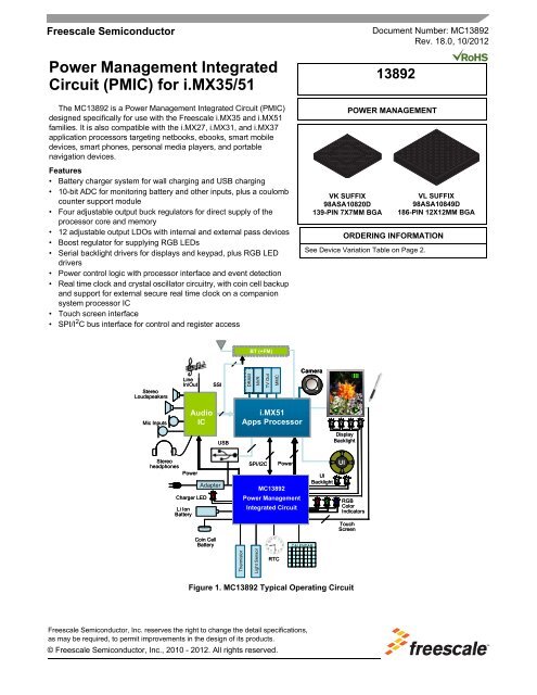
Stereo<br />
Loudspeakers<br />
Mic Inputs<br />
Line<br />
In/Out<br />
Stereo<br />
headphones<br />
<strong>Power</strong><br />
Li Ion<br />
Battery<br />
Audio<br />
IC<br />
Aud AP<br />
Charger LED<br />
Adapter<br />
USB<br />
BT (+FM)<br />
DRAM<br />
NVR<br />
TV IRDA Out<br />
i.MX51<br />
Apps Processor<br />
SPI/I2C<br />
<strong>MC13892</strong><br />
<strong>Power</strong> <strong>Power</strong> <strong>Management</strong><br />
Mgmt &<br />
User <strong>Integrated</strong> Interface AP <strong>Circuit</strong><br />
Aud& Pwr Mgmt<br />
CALENDAR<br />
Figure 1. <strong>MC13892</strong> Typical Operating <strong>Circuit</strong><br />
Freescale Semiconductor, Inc. reserves the right to change the detail specifications,<br />
as may be required, to permit improvements in the design of its products.<br />
© Freescale Semiconductor, Inc., 2010 - 2012. All rights reserved.<br />
SSI<br />
Coin Cell<br />
Battery<br />
Thermistor<br />
Light Sensor<br />
MMC<br />
RTC<br />
<strong>Power</strong><br />
VK SUFFIX<br />
98ASA10820D<br />
139-PIN 7X7MM BGA<br />
Document Number: <strong>MC13892</strong><br />
Rev. 18.0, 10/2012<br />
13892<br />
POWER MANAGEMENT<br />
VL SUFFIX<br />
98ASA10849D<br />
186-PIN 12X12MM BGA<br />
ORDERING INFORMATION<br />
See Device Variation Table on Page 2.<br />
Camera<br />
Camera<br />
UI<br />
Backlight<br />
Display<br />
Backlight<br />
UI<br />
RGB<br />
Color<br />
Indicators<br />
Touch<br />
Screen
DEVICE VARIATIONS<br />
Table 1. <strong>MC13892</strong> Device Variations<br />
<strong>MC13892</strong><br />
Part Number (1) Notes Package<br />
<strong>MC13892</strong>CJVK<br />
<strong>MC13892</strong>AJVK<br />
<strong>MC13892</strong>DJVK<br />
<strong>MC13892</strong>BJVK<br />
<strong>MC13892</strong>VK<br />
<strong>MC13892</strong>JVK<br />
<strong>MC13892</strong>CJVL<br />
<strong>MC13892</strong>AJVL<br />
<strong>MC13892</strong>DJVL<br />
<strong>MC13892</strong>BJVL<br />
<strong>MC13892</strong>VL<br />
<strong>MC13892</strong>JVL<br />
(2)<br />
(3)<br />
(2) (4)<br />
(3)<br />
(3)<br />
(3)<br />
(2)<br />
(3)<br />
(2) (4)<br />
(3)<br />
(3)<br />
(3)<br />
DEVICE VARIATIONS<br />
139-PIN<br />
7x7 mm BGA<br />
186-PIN<br />
12x12 mm BGA<br />
Temperature<br />
Range (T A )<br />
-40 to +85 °C<br />
Pin Map Description<br />
Figure 3<br />
Figure 4<br />
Global Reset Function Default ON<br />
Global Reset Function Default OFF<br />
No Global Reset Function<br />
Global Reset Function Default ON<br />
Global Reset Function Default OFF<br />
No Global Reset Function<br />
Notes<br />
1. For Tape and Reel product, add an “R2” suffix to the part number.<br />
2. Recommended <strong>for</strong> all new designs<br />
3. Not recommended <strong>for</strong> new designs<br />
4. Backward compatible replacement part <strong>for</strong> <strong>MC13892</strong>VK, <strong>MC13892</strong>JVK, <strong>MC13892</strong>VL, <strong>MC13892</strong>JVL, <strong>MC13892</strong>BJVK, and<br />
<strong>MC13892</strong>BJVL<br />
Analog <strong>Integrated</strong> <strong>Circuit</strong> Device Data<br />
2 Freescale Semiconductor
GNDADC<br />
ADIN5<br />
ADIN6<br />
ADIN7<br />
TSX1<br />
TSX2<br />
TSY1<br />
TSY2<br />
TSREF<br />
ADTRIG<br />
BATTISNSCC<br />
CFP<br />
CFM<br />
SPIVCC<br />
CS<br />
CLK<br />
MOSI<br />
MISO<br />
GNDSPI<br />
VCORE<br />
VCOREDIG<br />
REFCORE<br />
GNDCORE<br />
UID<br />
UVBUS<br />
VBUSEN<br />
VINUSB<br />
VUSB<br />
LICELL<br />
BATT<br />
BATTISNS<br />
BP<br />
BATTFET<br />
BP<br />
Battery Interface &<br />
Protection<br />
Voltage /<br />
Current<br />
Sensing &<br />
Translation<br />
Touch<br />
Screen<br />
Interface<br />
BATT<br />
SPI<br />
Interface<br />
+<br />
Muxed<br />
I2C<br />
Optional<br />
Interface<br />
Reference<br />
Generation<br />
OTG<br />
5V<br />
Connector<br />
Interface<br />
Li Cell<br />
Charger<br />
MUX<br />
VUSB<br />
Regulator<br />
BPSNS<br />
LCELL<br />
Switch<br />
CHRGISNS<br />
10 Bit GP<br />
ADC<br />
XTAL1<br />
CHRGCTRL1<br />
LICELL, UID, Die Temp, GPO4<br />
Coulomb<br />
Counter<br />
VBUS/ID<br />
Detectors<br />
GNDSUB1<br />
GNDSUB2<br />
GNDSUB3<br />
GNDSUB4<br />
GNDSUB5<br />
GNDSUB6<br />
GNDSUB7<br />
GNDSUB8<br />
GNDSUB9<br />
Trigger<br />
Handling<br />
CHRGCTRL2<br />
CCOUT To SPI<br />
Shift Register<br />
SPI<br />
Registers<br />
Shift Register<br />
32 KHz<br />
Internal<br />
Osc<br />
32 KHz<br />
Crystal<br />
Osc<br />
GNDRTC<br />
XTAL2<br />
CHRGRAW<br />
A/D Result<br />
A/D<br />
Control<br />
CHRGLED<br />
Charger Interface and Control:<br />
4 bit DAC, Clamp, Protection,<br />
Trickle Generation<br />
GNDCTRL<br />
MODE<br />
PUMS2<br />
PUMS1<br />
INTERNAL BLOCK DIAGRAM<br />
CHRGSE1B<br />
To Enables & Control<br />
SPI<br />
Control<br />
Logic<br />
PUMS<br />
GNDCHRG<br />
Trim-In-Package<br />
Startup<br />
Sequencer<br />
Decode<br />
Trim?<br />
SPI Result<br />
Registers<br />
Interrupt<br />
Inputs<br />
PWRON1<br />
PWRON2<br />
PWRON3<br />
STANDBY<br />
INT<br />
WDI<br />
Die Temp &<br />
Thermal Warning<br />
Detection<br />
Package Pin Legend<br />
<strong>MC13892</strong><br />
IC<br />
To<br />
Trimmed<br />
<strong>Circuit</strong>s<br />
Control<br />
Logic<br />
Output Pin<br />
Input Pin<br />
Bi-directional Pin<br />
Enables &<br />
Control<br />
Core Control Logic, Timers, & Interrupts<br />
RESETBMCU<br />
LEDMD<br />
LEDAD<br />
Backlight<br />
LED Drive<br />
RESETB<br />
STANDBYSEC<br />
Monitor<br />
Timer<br />
RTC +<br />
Calibration<br />
Figure 2. <strong>MC13892</strong> Simplified Internal Block Diagram<br />
INTERNAL BLOCK DIAGRAM<br />
<strong>MC13892</strong><br />
Analog <strong>Integrated</strong> <strong>Circuit</strong> Device Data<br />
Freescale Semiconductor 3<br />
LEDKP<br />
<strong>MC13892</strong><br />
To Interrupt<br />
Section<br />
CLK32K<br />
GNDBL<br />
PLL<br />
32 KHz<br />
Buffers<br />
CLK32KMCU<br />
Switchers<br />
LICELL<br />
BP<br />
VSRTC<br />
Best<br />
of<br />
Supply<br />
VSRTC<br />
LEDR<br />
LEDG<br />
LEDB<br />
Tri-Color<br />
LED Drive<br />
GNDLED<br />
SW1<br />
1050 mA<br />
Buck<br />
SW2<br />
800 mA<br />
Buck<br />
SW3<br />
800 mA<br />
Buck<br />
SW4<br />
800 mA<br />
Buck<br />
DVS<br />
CONTROL<br />
SWBST<br />
300 mA<br />
Boost<br />
SPI Control<br />
VVIDEO<br />
VUSB2<br />
VAUDIO<br />
VIOHI<br />
VPLL<br />
VDIG<br />
VCAM<br />
VSD<br />
VGEN1<br />
VGEN2<br />
VGEN3<br />
GPO<br />
Control<br />
GPO1<br />
GPO2<br />
GPO3<br />
GPO4<br />
PWR Gate<br />
Drive & Chg<br />
Pump<br />
O/P<br />
Drive<br />
O/P<br />
Drive<br />
SW1IN<br />
SW1OUT<br />
GNDSW1<br />
SW1FB<br />
SW2IN<br />
SW2OUT<br />
GNDSW2<br />
SW2FB<br />
SW3IN<br />
O/P SW3OUT<br />
Drive GNDSW3<br />
SW3FB<br />
O/P<br />
Drive<br />
PWGTDRV1<br />
PWGTDRV2<br />
SW4IN<br />
O/P SW4OUT<br />
Drive GNDSW4<br />
SW4FB<br />
Pass<br />
FET<br />
Pass<br />
FET<br />
Pass<br />
FET<br />
Pass<br />
FET<br />
Pass<br />
FET<br />
Pass<br />
FET<br />
Pass<br />
FET<br />
DVS1<br />
DVS2<br />
SWBSTIN<br />
SWBSTOUT<br />
SWBSTFB<br />
GNDSWBST<br />
VVIDEODRV<br />
VVIDEO<br />
VINUSB2<br />
VUSB2<br />
VINAUDIO<br />
VAUDIO<br />
VINIOHI<br />
VIOHI<br />
VINPLL<br />
VPLL<br />
VINDIG<br />
VDIG<br />
VINCAMDRV<br />
VCAM<br />
VSDDRV<br />
VSD<br />
VGEN1DRV<br />
VGEN1<br />
VGEN2DRV<br />
VGEN2<br />
VINGEN3DRV<br />
VGEN3<br />
GNDREG1<br />
GNDREG2<br />
GNDREG3
PIN CONNECTIONS<br />
<strong>MC13892</strong><br />
PIN CONNECTIONS<br />
1 2 3 4 5 6 7 8 9 10 11 12 13<br />
A VUSB2 VUSB2 VINUSB2 SWBSTIN GNDSWBST GNDBL NC MODE VCORE BATT CHRGRAW CHRGCTRL2 CHRGCTRL2<br />
B VUSB2 GPO1 DVS2 SWBSTOUT LEDB LEDKP LEDR GNDCORE VCOREDIG BP CHRGCTRL1 BATTISNSCC CHRGCTRL2<br />
C VINPLL VSDDRV CHRGISNS BATTISNS<br />
D VUSB VSD SWBSTFB LEDMD DVS1 REFCORE CHRGSE1B LICELL BATTFET BPSNS PWRON1<br />
E UVBUS VPLL LEDG GNDLED UID PUMS2 GNDCHRG CHRGLED PWRON2 ADTRIG INT GNDSW1<br />
F GNDSW3 VBUSEN SW3FB LEDAD GNDSUB GNDSUB GNDSUB GPO3 GPO2 RESETBMCU RESETB SW1OUT<br />
G SW3OUT VINUSB SW4FB GNDREG2 GNDSUB GNDSUB GNDSUB PUMS1 WDI GPO4 SW1IN<br />
H SW3IN MISO GNDSPI GNDREG3 GNDSUB GNDSUB GNDSUB GNDCTRL SW1FB STANDBYSEC SW2IN<br />
J SW4IN MOSI CLK32KMCU STANDBY GNDADC GNDREG1 PWRON3 TSX1 SW2FB TSX2 SW2OUT<br />
K SW4OUT SPIVCC PWGTDRV1 CLK32K VCAM CFP CFM ADIN5 ADIN6 VVIDEODRV GNDSW2<br />
L GNDSW4 CS TSY2 VVIDEO<br />
M VGEN3 CLK VGEN2 VSRTC GNDRTC VINCAMDRV PWGTDRV2 VDIG VINDIG VGEN1DRV ADIN7 TSY1 TSREF<br />
N VGEN3 VGEN3 VINGEN3DRV VGEN2DRV XTAL2 XTAL1 VINAUDIO VAUDIO VIOHI VINIOHI VGEN1 TSREF TSREF<br />
Figure 3. <strong>MC13892</strong>VK Pin Connections<br />
Analog <strong>Integrated</strong> <strong>Circuit</strong> Device Data<br />
4 Freescale Semiconductor<br />
Regulators<br />
Switchers<br />
Backlights<br />
Control Logic<br />
Charger<br />
RTC<br />
Grounds<br />
USB<br />
ADC<br />
SPI/I2C<br />
No Connect
1 2 3 4 5 6 7 8 9 10 11 12 13 14<br />
PIN CONNECTIONS<br />
A VUSB2 VINUSB2 SWBSTOUT SWBSTIN GNDSUB NC MODE VCORE BATT CHRGRAW CHRGCTRL2 CHRGISNS Regulators<br />
B VSDDRV GPO1 GNDSUB GNDSUB LEDR UID DVS1 REFCORE GNDCORE CHRGSE1B BP GNDCHRG BATTISNSCC BATTISNS Switchers<br />
C VSD DVS2 SWBSTFB LEDB LEDG LEDKP LEDAD PUMS2 VCOREDIG LICELL BATTFET BPSNS GPO3 PUMS1 Backlights<br />
D VUSB VPLL GNDSUB GNDSUB GNDSWBST GNDLED LEDMD GNDBL CHRGCTRL1 CHRGLED PWRON1 PWRON3 ADTRIG GPO4 Control Logic<br />
E UVBUS GNDREG2 VINPLL GNDSUB GNDSUB GNDSUB GNDSUB GNDSUB GNDSUB GNDSUB PWRON2 GPO2 INT RESETBMCU Charger<br />
F SW3OUT VBUSEN VINUSB GNDSUB GNDSUB GNDSUB GNDSUB GNDSUB GNDSUB GNDSUB GNDCTRL WDI RESETB SW1OUT RTC<br />
G GNDSW3 GNDSW3 SW3FB GNDSUB GNDSUB GNDSUB GNDSUB GNDSUB GNDSUB GNDSUB GNDSUB SW1FB GNDSW1 GNDSW1 Grounds<br />
H SW3IN SW3IN GNDSUB GNDSUB GNDSUB GNDSUB GNDSUB GNDSUB GNDSUB GNDSUB SW1IN SW1IN USB<br />
J SW4IN SW4IN SW4FB GNDSUB GNDSUB GNDSUB GNDSUB GNDSUB GNDSUB SW2FB SW2IN SW2IN ADC<br />
K GNDSW4 GNDSW4 SPIVCC GNDSUB GNDSUB GNDSUB GNDSUB GNDSUB GNDSUB VVIDEODRV GNDSW2 GNDSW2 SPI/I2C<br />
L SW4OUT CS GNDSPI GNDSUB GNDSUB GNDSUB VCAM VINAUDIO VDIG GNDSUB TSY2 STANDBYSEC VVIDEO SW2OUT No Connect<br />
M CLK VINGEN3DRV CLK32KMCU CLK32K VSRTC STANDBY VINCAMDRV CFP CFM VGEN1DRV VGEN1 TSX1 TSX2 TSY1<br />
N VGEN3 MOSI VGEN2 GNDREG3 XTAL2 XTAL1 VAUDIO PWGTDRV2 VIOHI VINIOHI GNDADC ADIN5 ADIN7 TSREF<br />
P MISO PWGTDRV1 VGEN2DRV GNDSUB GNDRTC GNDSUB GNDSUB GNDSUB GNDSUB VINDIG GNDREG1 ADIN6<br />
Figure 4. <strong>MC13892</strong>VL Pin Connections<br />
<strong>MC13892</strong><br />
Analog <strong>Integrated</strong> <strong>Circuit</strong> Device Data<br />
Freescale Semiconductor 5
PIN CONNECTIONS<br />
Table 2. <strong>MC13892</strong> Pin Definitions<br />
A functional description of each pin can be found in the Functional Description.<br />
Pin Number<br />
on the<br />
13982VK<br />
7x7 mm<br />
<strong>MC13892</strong><br />
Pin Number on<br />
the 13982VL<br />
12x12 mm<br />
Pin Name<br />
Rating<br />
(V)<br />
Pin Function Formal Name Definition<br />
A1, A2, B1 A2 VUSB2 3.6 Output USB 2 Supply Output regulator <strong>for</strong> USB PHY<br />
A3 A3 VINUSB2 5.5 <strong>Power</strong> USB 2 Supply Input Input regulator VUSB2<br />
A4 A5 SWBSTIN 5.5 <strong>Power</strong> Switcher Boost <strong>Power</strong><br />
Input<br />
Switcher BST input<br />
A5 D5 GNDSWBST – Ground Switcher Boost Ground Ground <strong>for</strong> switcher BST<br />
A6 D8 GNDBL – Ground Backlight LED Ground Ground <strong>for</strong> serial LED drive<br />
A7 A7 NC – – No Connect Do not connect<br />
A8 A8 MODE 9.0 Input Mode Configuration USB LBP mode, normal mode, test mode<br />
selection,& anti-fuse bias<br />
A9 A9 VCORE 3.6 Output Core Supply Regulated supply output <strong>for</strong> the IC analog<br />
core circuitry<br />
A10 A10 BATT 5.5 Input Battery Connection 1. Battery positive pin<br />
2. Battery current sensing point 2<br />
3. Battery supply voltage sense<br />
A11 A11 CHRGRAW 20 I/O Charger Input 1. Charger input<br />
2. Output to battery supplied accesories<br />
A12, A13, B13 A12 CHRGCTRL2 5.5 Output Charger Control 2 Driver output <strong>for</strong> charger path FETs M2<br />
B2 B2 GPO1 3.6 Output General Purpose<br />
Output 1<br />
B3 C2 DVS2 3.6 Input Dynamic Voltage<br />
Scaling Control 2<br />
General purpose output 1<br />
Switcher 2 DVS input pin<br />
B4 A4 SWBSTOUT 7.5 <strong>Power</strong> Switcher Boost Output Switcher BST BP supply<br />
B5 C4 LEDB 7.5 Input LED Driver General purpose LED current sink driver<br />
Blue<br />
B6 C6 LEDKP 28 Input LED Driver Keypad lighting LED current sink driver<br />
B7 B5 LEDR 7.5 Input LED Driver General purpose LED current sink driver Red<br />
B8 B9 GNDCORE – Ground Core Ground Ground <strong>for</strong> the IC core circuitry<br />
B9 C9 VCOREDIG 1.5 Output Digital Core Supply Regulated supply output <strong>for</strong> the IC digital<br />
core circuitry<br />
B10 B11 BP 5.5 <strong>Power</strong> Battery Plus 1. Application supply point<br />
2. Input supply to the IC core circuitry<br />
3. Application supply voltage sense<br />
B11 D9 CHRGCTRL1 20 Output Charger Control 1 Driver output <strong>for</strong> charger path FETs M1<br />
B12 B13 BATTISNSCC 4.8 Input Battery Current Sense Accumulated current counter current sensing<br />
point<br />
C1 E3 VINPLL 5.5 <strong>Power</strong> PLL Supply Input Input regulator processor PLL<br />
C2 B1 VSDDRV 5.5 Output VSD Driver Drive output regulated SD card<br />
C12 A13 CHRGISNS 4.8 Input Charger Current Sense Charge current sensing point 1<br />
C13 B14 BATTISNS 4.8 Input Battery Current Sense Battery current sensing point 1<br />
Analog <strong>Integrated</strong> <strong>Circuit</strong> Device Data<br />
6 Freescale Semiconductor
Table 2. <strong>MC13892</strong> Pin Definitions (continued)<br />
A functional description of each pin can be found in the Functional Description.<br />
Pin Number<br />
on the<br />
13982VK<br />
7x7 mm<br />
Pin Number on<br />
the 13982VL<br />
12x12 mm<br />
D1 D1 VUSB 3.6 Output USB Supply USB transceiver regulator output<br />
D2 C1 VSD 3.6 Output SD Card Supply Output regulator SD card<br />
D4 C3 SWBSTFB 3.6 Input Switcher Boost<br />
Feedback<br />
Switcher BST feedback<br />
PIN CONNECTIONS<br />
D5 D7 LEDMD 28 Input LED Driver Main display backlight LED current sink<br />
driver<br />
D6 B7 DVS1 3.6 Input Dynamic Voltage<br />
Scaling Control 1<br />
Switcher 1DVS input pin<br />
D7 B8 REFCORE 3.6 Output Core Reference Main bandgap reference<br />
D8 B10 CHRGSE1B 3.6 Input Charger Select Charger <strong>for</strong>ced SE1 detection input<br />
D9 C10 LICELL 3.6 I/O Coin Cell Connection 1. Coin cell supply input<br />
2. Coin cell charger output<br />
D10 C11 BATTFET 4.8 Output Battery FET<br />
Connection<br />
Driver output <strong>for</strong> battery path FET M3<br />
D12 C12 BPSNS 4.8 Input Battery Plus Sense 1. BP sense point<br />
2. Charge current sensing point 2<br />
D13 D11 PWRON1 3.6 Input <strong>Power</strong> On 1 <strong>Power</strong> on/off button connection 1<br />
E1 E1 UVBUS 20 I/O USB Bus 1. USB transceiver cable interface<br />
2. VBUS & OTG supply output<br />
E2 D2 VPLL 3.6 Output Voltage Supply <strong>for</strong> PLL Output regulator processor PLL<br />
E4 C5 LEDG 7.5 Input PWM Driver <strong>for</strong> Green<br />
LED<br />
General purpose LED current sink driver<br />
Green<br />
E5 D6 GNDLED – Ground LED Ground Ground <strong>for</strong> LED drivers<br />
E6 B6 UID 5.5 Input USB ID USB OTG transceiver cable ID<br />
E7 C8 PUMS2 3.6 Input <strong>Power</strong> Up Mode Select<br />
2<br />
<strong>Power</strong> up mode supply setting 2<br />
E8 B12 GNDCHRG – Ground Charger Ground Ground <strong>for</strong> charger interface<br />
E9 D10 CHRGLED 20 Output Charger LED Trickle LED driver output 1<br />
E10 E11 PWRON2 3.6 Input <strong>Power</strong> On 2 <strong>Power</strong> on/off button connection 2<br />
E11 D13 ADTRIG 3.6 Input ADC Trigger ADC trigger input<br />
E12 E13 INT 3.6 Output Interrupt Signal Interrupt to processor<br />
E13 G13, G14 GNDSW1 – Ground Switcher 1 Ground Ground <strong>for</strong> switcher 1<br />
F1 G1, G2 GNDSW3 – Ground Switcher 3 Ground Ground <strong>for</strong> switcher 3<br />
F2 F2 VBUSEN 3.6 Input VBUS Enable External VBUS enable pin <strong>for</strong> OTG supply<br />
F4 G3 SW3FB 3.6 Input Switcher 3 Feedback Switcher 3 feedback<br />
F5 C7 LEDAD 28 Input Auxiliary Display LED Auxiliary display backlight LED sinking<br />
current driver<br />
F6 A6, B3, B4, D3,<br />
D4, E4, E5, E6<br />
Pin Name<br />
Rating<br />
(V)<br />
Pin Function Formal Name Definition<br />
GNDSUB1 – Ground Ground 1 Non critical signal ground and thermal heat<br />
sink<br />
<strong>MC13892</strong><br />
Analog <strong>Integrated</strong> <strong>Circuit</strong> Device Data<br />
Freescale Semiconductor 7
PIN CONNECTIONS<br />
Table 2. <strong>MC13892</strong> Pin Definitions (continued)<br />
A functional description of each pin can be found in the Functional Description.<br />
Pin Number<br />
on the<br />
13982VK<br />
7x7 mm<br />
<strong>MC13892</strong><br />
Pin Number on<br />
the 13982VL<br />
12x12 mm<br />
F7 E7, E8, E9, E10,<br />
F4, F5, F6<br />
F8 F7, F8, F9, F10,<br />
G4, G5, G6, G7,<br />
G8<br />
GNDSUB2 – Ground Ground 2 Non critical signal ground and thermal heat<br />
sink<br />
GNDSUB3 – Ground Ground 3 Non critical signal ground and thermal heat<br />
sink<br />
F9 C13 GPO3 – Output General Purpose<br />
Output 3<br />
F10 E12 GPO2 3.6 Output General Purpose<br />
Output 2<br />
General purpose output 3<br />
General purpose output 2<br />
F11 E14 RESETBMCU 3.6 Output MCU Reset Reset output <strong>for</strong> processor<br />
F12 F13 RESETB 3.6 Output Peripheral Reset Reset output <strong>for</strong> peripherals<br />
F13 F14 SW1OUT 5.5 Output Switcher 1 Output Switcher 1 output<br />
G1 F1 SW3OUT 5.5 Output Switcher 3 Output Switcher 3 output<br />
G2 F3 VINUSB 7.5 Input VUSB Supply Input Input option <strong>for</strong> UVUSB; tie to SWBST at top<br />
level<br />
G4 J3 SW4FB 3.6 Input Switcher 4 Feedback Switcher 4 feedback<br />
G5 E2 GNDREG2 – Ground Regulator 2 Ground Ground <strong>for</strong> regulators 2<br />
G6 G9, G10, G11,<br />
H3, H5, H6, H7,<br />
H8<br />
G7 H9, H10, H12,<br />
J5, J6, J7<br />
G8 J8, J9, J10, K4,<br />
K5, K6, K7<br />
GNDSUB4 – Ground Ground 4 Non critical signal ground and thermal heat<br />
sink<br />
GNDSUB5 – Ground Ground 5 Non critical signal ground and thermal heat<br />
sink<br />
GNDSUB6 – Ground Ground 6 Non critical signal ground and thermal heat<br />
sink<br />
G9 C14 PUMS1 3.6 Input <strong>Power</strong> Up Mode Select<br />
1<br />
G10 F12 WDI 3.6 Input Watchdog Input Watchdog input<br />
G12 D14 GPO4 3.6 Output General Purpose<br />
Output 4<br />
<strong>Power</strong> up mode supply setting 1<br />
General purpose output 4<br />
G13 H13, H14 SW1IN 5.5 Input Switcher 1 Input Input voltage <strong>for</strong> switcher 1<br />
H1 H1, H2 SW3IN 5.5 <strong>Power</strong> Switcher 3 Input Switcher 3 input<br />
H2 P2 MISO 3.6 I/O Master In Slave Out Primary SPI read output<br />
H4 L3 GNDSPI – Ground SPI Ground Ground <strong>for</strong> SPI interface<br />
H5 N4 GNDREG3 – Ground Regulator 3 Ground Ground <strong>for</strong> regulators 3<br />
H6 K8, K10, L4, L5,<br />
L6, L10<br />
H7 P5, P7, P8, P9,<br />
P10<br />
Pin Name<br />
Rating<br />
(V)<br />
Pin Function Formal Name Definition<br />
GNDSUB7 – Ground Ground 7 Non critical signal ground and thermal heat<br />
sink<br />
GNDSUB8 – Ground Ground 8 Non critical signal ground and thermal heat<br />
sink<br />
H8 – GNDSUB9 – Ground Ground 9 Non critical signal ground and thermal heat<br />
sink<br />
H9 F11 GNDCTRL – Ground Logic Control Ground Ground <strong>for</strong> control logic<br />
Analog <strong>Integrated</strong> <strong>Circuit</strong> Device Data<br />
8 Freescale Semiconductor
Table 2. <strong>MC13892</strong> Pin Definitions (continued)<br />
A functional description of each pin can be found in the Functional Description.<br />
Pin Number<br />
on the<br />
13982VK<br />
7x7 mm<br />
Pin Number on<br />
the 13982VL<br />
12x12 mm<br />
Pin Name<br />
Rating<br />
(V)<br />
Pin Function Formal Name Definition<br />
H10 G12 SW1FB 3.6 Input Switcher 1 Feedback Switcher 1 feedback<br />
H12 L12 STANDBYSEC 3.6 Input Secondary Standby<br />
Signal<br />
PIN CONNECTIONS<br />
Standby input signal from peripherals<br />
H13 J13, J14 SW2IN 5.5 Input Switcher 2 Input Input voltage <strong>for</strong> Switcher 2<br />
J1 J1, J2 SW4IN 5.5 <strong>Power</strong> Switcher 4 Input Switcher 4 input<br />
J2 N2 MOSI 3.6 Input Master Out Slave In Primary SPI write input<br />
J4 M3 CLK32KMCU 3.6 Output 32 kHz Clock <strong>for</strong> MCU 32 kHz clock output <strong>for</strong> processor<br />
J5 M6 STANDBY 3.6 Input Standby Signal Standby input signal from processor<br />
J6 N11 GNDADC – Ground ADC Ground Ground <strong>for</strong> A to D circuitry<br />
J7 P12 GNDREG1 – Ground Regulator 1 Ground Ground <strong>for</strong> regulators 1<br />
J8 D12 PWRON3 3.6 Input <strong>Power</strong> On 3 <strong>Power</strong> on/off button connection 3<br />
J9 M12 TSX1 3.6 Input Touch Screen<br />
Interface X1<br />
Touch screen interface X1<br />
J10 J12 SW2FB 3.6 Input Switcher 2 Feedback Switcher 2 feedback<br />
J12 M13 TSX2 3.6 Input Touch Screen<br />
Interface X2<br />
Touch screen interface X2<br />
J13 L14 SW2OUT 5.5 Output Switcher 2 Output Switcher 2 output<br />
K1 L1 SW4OUT 5.5 Output Switcher 4 Output Switcher 4 output<br />
K2 K3 SPIVCC 3.6 Input Supply Voltage <strong>for</strong> SPI Supply <strong>for</strong> SPI bus and audio bus<br />
K4 P3 PWGTDRV1 4.8 Output <strong>Power</strong> Gate Driver 1 <strong>Power</strong> gate driver 1<br />
K5 M4 CLK32K 3.6 Output 32 kHz Clock 32 kHz clock output <strong>for</strong> peripherals<br />
K6 L7 VCAM 3.6 Output Camera Supply Output regulator camera<br />
K7 M8 CFP 4.8 Passive Current Filter Positive Accumulated current filter cap plus pin<br />
K8 M9 CFM 4.8 Passive Current Filter Negative Accumulated current filter cap minus pin<br />
K9 N12 ADIN5 4.8 Input ADC Channel 5 Input ADC generic input channel 5<br />
K10 P13 ADIN6 4.8 Input ADC Channel 6 Input ADC generic input channel 6<br />
K12 K12 VVIDEODRV 5.5 Output VVIDEO Driver Drive output regulator VVIDEO<br />
K13 K13, K14 GNDSW2 – Ground Switcher 2 Ground Ground <strong>for</strong> switcher 2<br />
L1 K1, K2 GNDSW4 – Ground Switcher 4 Ground Ground <strong>for</strong> switcher 4<br />
L2 L2 CS 3.6 Input Chip Select Primary SPI select input<br />
L12 L11 TSY2 3.6 Input Touch Screen<br />
Interface Y2<br />
Touch screen interface Y2<br />
L13 L13 VVIDEO 3.6 Output Video Supply Output regulator TV DAC<br />
M1, N1, N2 N1 VGEN3 3.6 Output General Purpose<br />
Regulator 3<br />
Output GEN3 regulator<br />
M2 M1 CLK 3.6 Input Clock Primary SPI clock input<br />
M3 N3 VGEN2 3.6 Output General Purpose<br />
Regulator 2<br />
Output GEN2 regulator<br />
<strong>MC13892</strong><br />
Analog <strong>Integrated</strong> <strong>Circuit</strong> Device Data<br />
Freescale Semiconductor 9
PIN CONNECTIONS<br />
Table 2. <strong>MC13892</strong> Pin Definitions (continued)<br />
A functional description of each pin can be found in the Functional Description.<br />
Pin Number<br />
on the<br />
13982VK<br />
7x7 mm<br />
<strong>MC13892</strong><br />
M4 M5 VSRTC 3.6 Output SRTC Supply Output regulator <strong>for</strong> SRTC module on<br />
processor<br />
M5 P6 GNDRTC – Ground Real Time Clock<br />
Ground<br />
M6 M7 VINCAMDRV 5.5 I/O Camera Regulator<br />
Supply Input and Driver<br />
Output<br />
Ground <strong>for</strong> the RTC block<br />
M7 N8 PWGTDRV2 4.8 Output <strong>Power</strong> Gate Driver 2 <strong>Power</strong> gate driver 2<br />
1. Input regulator camera using internal<br />
PMOS FET.<br />
2. Drive output regulator <strong>for</strong> camera voltage<br />
using external PNP device.<br />
M8 L9 VDIG 3.6 Output Digital Supply Output regulator digital<br />
M9 P11 VINDIG 5.5 Input VDIG Supply Input Input regulator digital<br />
M10 M10 VGEN1DRV 5.5 Output VGEN1 Driver Drive output GEN1 regulator<br />
M11 N13 ADIN7 4.8 Input ADC Channel 7 Input ADC generic input channel 7, group 1<br />
M12 M14 TSY1 3.6 Input Touch Screen<br />
Interface Y1<br />
M13, N12,<br />
N13<br />
Pin Number on<br />
the 13982VL<br />
12x12 mm<br />
Pin Name<br />
Rating<br />
(V)<br />
Pin Function Formal Name Definition<br />
N14 TSREF 3.6 Output Touch Screen<br />
Reference<br />
N3 M2 VINGEN3DRV 5.5 <strong>Power</strong>/Output VGEN3 Supply Input<br />
and Driver Output<br />
Touch screen interface Y1<br />
Touch screen reference<br />
1. Input VGEN3 regulator<br />
2. Drive VGEN3 output regulator<br />
N4 P4 VGEN2DRV 5.5 Output VGEN2 Driver Drive output GEN2 regulator<br />
N5 N5 XTAL2 2.5 Input Crystal Connection 2 32.768 kHz oscillator crystal connection 2<br />
N6 N6 XTAL1 2.5 Input Crystal Connection 1 32.768 kHz oscillator crystal connection 1<br />
N7 L8 VINAUDIO 5.5 <strong>Power</strong> Audio Supply Input Input regulator VAUDIO<br />
N8 N7 VAUDIO 3.6 Output Audio Supply Output regulator <strong>for</strong> audio<br />
N9 N9 VIOHI 3.6 Output High Voltage IO Supply Output regulator high voltage IO, efuse<br />
N10 N10 VINIOHI 5.5 Input High Voltage IO Supply<br />
Input<br />
N11 M11 VGEN1 3.6 Output General Purpose<br />
Regulator 1<br />
Input regulator high voltage IO<br />
Input GEN1 regulator<br />
Analog <strong>Integrated</strong> <strong>Circuit</strong> Device Data<br />
10 Freescale Semiconductor
Table 3. Maximum Ratings<br />
ELECTRICAL CHARACTERISTICS<br />
MAXIMUM RATINGS<br />
ELECTRICAL CHARACTERISTICS<br />
MAXIMUM RATINGS<br />
All voltages are with respect to ground unless otherwise noted. Exceeding these ratings may cause a malfunction or<br />
permanent damage to the device.<br />
ELECTRICAL RATINGS<br />
Charger and USB Input Voltage (5)<br />
Ratings Symbol Value Unit<br />
V CHRGR -0.3 to 20 V<br />
MODE pin Voltage V MODE -0.3 to 9.0 V<br />
Main/Aux/Keypad Current Sink Voltage VLEDMD, VLEDAD, VLEDKP -0.3 to 28 V<br />
Battery Voltage VBATT -0.3 to 4.8 V<br />
Coin Cell Voltage V LICELL -0.3 to 3.6 V<br />
ESD Voltage (6)<br />
Human Body Model - HBM with Mode pin excluded (9)<br />
Charge Device Model - CDM<br />
THERMAL RATINGS<br />
Ambient Operating Temperature Range T A -40 to +85 °C<br />
Operating Junction Temperature Range T J -40 to +125 °C<br />
Storage Temperature Range T STG -65 to +150 °C<br />
THERMAL RESISTANCE<br />
Peak Package Reflow Temperature During Reflow (7) , (8)<br />
<strong>MC13892</strong><br />
Analog <strong>Integrated</strong> <strong>Circuit</strong> Device Data<br />
Freescale Semiconductor 11<br />
V ESD<br />
±1500<br />
±250<br />
T PPRT Note 8 °C<br />
Notes<br />
5. USB Input Voltage applies to UVBUS pin only<br />
6. ESD testing is per<strong>for</strong>med in accordance with the Human Body Model (HBM) (CZAP = 100 pF, RZAP = 1500 Ω) and the Charge Device<br />
Model (CDM), Robotic (CZAP = 4.0 pF).<br />
7. Pin soldering temperature limit is <strong>for</strong> 10 seconds maximum duration. Not designed <strong>for</strong> immersion soldering. Exceeding these limits may<br />
cause malfunction or permanent damage to the device.<br />
8. Freescale’s Package Reflow capability meets Pb-free requirements <strong>for</strong> JEDEC standard J-STD-020C. For Peak Package Reflow<br />
Temperature and Moisture Sensitivity Levels (MSL), Go to www.freescale.com, search by part number [e.g. remove prefixes/suffixes<br />
and enter the core ID to view all orderable parts. (i.e. MC33xxxD enter 33xxx), and review parametrics.<br />
9. Mode Pin is not ESD protected.<br />
Table 4. Dissipation Ratings<br />
Rating Parameter Condition Symbol VK Package VL Package Unit<br />
Junction to Ambient Natural Convection Single layer board (1s) R θJA 104 65 °C/W<br />
Junction to Ambient Natural Convection Four layer board (2s2p) R θJMA 54 42 °C/W<br />
Junction to Ambient (@200 ft/min) Single layer board (1s) R θJMA 88 55 °C/W<br />
Junction to Ambient (@200 ft/min) Four layer board (2s2p) R θJMA 49 38 °C/W<br />
Junction to Board R θJB 32 28 °C/W<br />
Junction to Case R θJC 29 22 °C/W<br />
Junction to Package Top Natural Convection θJT 7.0 5.0 °C/W<br />
V
ELECTRICAL CHARACTERISTICS<br />
STATIC ELECTRICAL CHARACTERISTICS<br />
Table 5. Static Electrical Characteristics<br />
<strong>MC13892</strong><br />
STATIC ELECTRICAL CHARACTERISTICS<br />
Characteristics noted under conditions - 40 °C ≤ T A ≤ 85 °C, GND = 0 V unless otherwise noted. Typical values noted reflect<br />
the approximate parameter means at T A = 25 °C under nominal conditions, unless otherwise noted.<br />
CURRENT CONSUMPTION<br />
Characteristic Symbol Min Typ Max Unit<br />
RTC Mode<br />
All blocks disabled, no main battery attached, coin cell is attached to<br />
LICELL (10)<br />
IRTC RTC<br />
– 3.00 6.00<br />
OFF Mode (All blocks disabled, main battery attached) (10)<br />
<strong>MC13892</strong> core and RTC module<br />
IOFF – 10 30<br />
<strong>Power</strong> Cut Mode (All blocks disabled, no main battery attached, coin cell<br />
is attached and valid) (10)<br />
IPCUT <strong>MC13892</strong> core and RTC module<br />
ON Standby mode - Low-power mode<br />
– 3.0 6.0<br />
4 buck regulators in low-power mode, 3 regulators (11) ISTBY – 230 295<br />
ON Mode - Typical use case<br />
4 buck regulators in PWMPS mode, 5 Regulators (12) ION – 459 1500<br />
I/O CHARACTERISTICS (13)<br />
PWRON1, PWRON2, PWRON3, Pull-up (14)<br />
Input Low, 47 kOhm<br />
Input High, 1.0 MOhm<br />
CHRGSE1B, Pull-up (15)<br />
Input Low<br />
Input High<br />
STANDBY, STANDBYSEC, WDI, ADTRIG, Weak Pull-down (16) , (17)<br />
Input Low<br />
Input High<br />
CLK32K, CMOS<br />
Output Low, -100 μA<br />
Output High, 100 μA<br />
CLK32KMCU, CMOS<br />
Output Low, -100 μA<br />
Output High, 100 μA<br />
RESETB, RESETBMCU, Open Drain (18)<br />
Output Low, -2.0 mA<br />
Output High, Open Drain<br />
Analog <strong>Integrated</strong> <strong>Circuit</strong> Device Data<br />
12 Freescale Semiconductor<br />
0.0<br />
1.0<br />
0.0<br />
1.0<br />
0.0<br />
1.0<br />
0.0<br />
SPIVCC -0.2<br />
0.0<br />
VSRTC- 0.2<br />
Notes<br />
10. Valid at 25 °C only.<br />
11. VPLL, VIOHI, VGEN2<br />
12. VPLL, VIOHI, VGEN2, VAUDIO, VVIDEO<br />
13. SPIVCC is typically connected to the output of buck regulator: SW4 and set to 1.800 V<br />
14. Input has internal pull-up to VCOREDIG equivalent to 200 kOhm<br />
15. Input has internal pull-up to VCORE equivalent to 100 kOhm<br />
16. SPIVCC needs to remain enabled <strong>for</strong> proper detection of WDI High to avoid involuntary shutdown<br />
17. A weak pull-down represents a nominal internal pull down of 100 nA, unless otherwise noted<br />
18. RESETB & RESETBMCU have open drain outputs, external pull-ups are required<br />
0.0<br />
0.0<br />
–<br />
–<br />
–<br />
–<br />
–<br />
–<br />
–<br />
–<br />
–<br />
–<br />
–<br />
–<br />
0.3<br />
VCOREDIG<br />
0.3<br />
VCORE<br />
0.3<br />
3.6<br />
0.2<br />
SPIVCC<br />
0.2<br />
VSRTC<br />
0.4<br />
3.6<br />
µA<br />
µA<br />
µA<br />
µA<br />
µA<br />
V<br />
V<br />
V<br />
V<br />
V<br />
V
I/O CHARACTERISTICS (CONTINUED) (19)<br />
ELECTRICAL CHARACTERISTICS<br />
STATIC ELECTRICAL CHARACTERISTICS<br />
Table 5. Static Electrical Characteristics (continued)<br />
Characteristics noted under conditions - 40 °C ≤ TA ≤ 85 °C, GND = 0 V unless otherwise noted. Typical values noted reflect<br />
the approximate parameter means at TA = 25 °C under nominal conditions, unless otherwise noted.<br />
VSRTC, Voltage Output 1.1 – 1.3 V<br />
DVS1, DVS2, Weak Pull-down (20)<br />
V<br />
Input Low<br />
0.0<br />
– 0.3* SPIVCC<br />
Input High<br />
0.7* SPIVCC –<br />
3.1<br />
GPO1, CMOS<br />
V<br />
Output Low, -400 μA<br />
0.0<br />
–<br />
0.2<br />
Output High, 400 μA<br />
VCORE- 0.2 – VCORE<br />
To VCORE<br />
200<br />
–<br />
500 Ohm<br />
GPO2, GPO3, GPO4, CMOS<br />
V<br />
Output Low, -100 μA<br />
0.0<br />
–<br />
0.2<br />
Output High, 100 μA<br />
VIOHI - 0.2 – VIOHI<br />
GPO4, Analog Input 0.0 – VCORE+0.3 V<br />
CS, CLK, MOSI, VBUSEN, Weak Pull-down on CS and VBUSEN (20)<br />
Input Low<br />
Input High<br />
CS, MOSI (at Booting <strong>for</strong> SPI / I 2 C decoding), Weak Pull-down on CS (21)<br />
Input Low<br />
Input High<br />
MISO, INT, CMOS (22)<br />
Output Low, -100 μA<br />
Output High, 100 μA<br />
PUMS1, PUMS2 (22)<br />
PUMSxS = 00<br />
PUMSxS = 01, Load < 10 pF<br />
PUMSxS = 10<br />
PUMSxS = 11<br />
MODE (23)<br />
Input Low<br />
Input Med<br />
Input High<br />
Characteristic Symbol Min Typ Max Unit<br />
<strong>MC13892</strong><br />
Analog <strong>Integrated</strong> <strong>Circuit</strong> Device Data<br />
Freescale Semiconductor 13<br />
0.0<br />
0.7* SPIVCC<br />
0.0<br />
0.7 * VCORE<br />
0.0<br />
SPIVCC -0.2<br />
0.0<br />
Open<br />
1.3<br />
2.5<br />
0.0<br />
1.1<br />
VCORE<br />
Notes<br />
19. SPIVCC is typically connected to the output of buck regulator: SW4 and set to 1.800 V<br />
20. A weak pull-down represents a nominal internal pull down of 100 nA unless otherwise noted<br />
21. The weak pull-down on CS is disabled if a VIH is detected at startup to avoid extra consumption in I 2 C mode<br />
22. The output drive strength is programmable<br />
23. Input state is latched in first phase of cold start, refer to <strong>Power</strong> Control System <strong>for</strong> description of PUMS configuration<br />
24. Input state is not latched<br />
–<br />
–<br />
–<br />
–<br />
–<br />
–<br />
–<br />
–<br />
–<br />
–<br />
–<br />
–<br />
–<br />
0.3* SPIVCC<br />
SPIVCC+0.3<br />
0.3 * VCORE<br />
VCORE<br />
0.2<br />
SPIVCC<br />
0.3<br />
Open<br />
2.0<br />
3.1<br />
0.4<br />
1.7<br />
9.0<br />
V<br />
V<br />
V<br />
V<br />
V
ELECTRICAL CHARACTERISTICS<br />
STATIC ELECTRICAL CHARACTERISTICS<br />
Table 5. Static Electrical Characteristics (continued)<br />
Characteristics noted under conditions - 40 °C ≤ TA ≤ 85 °C, GND = 0 V unless otherwise noted. Typical values noted reflect<br />
the approximate parameter means at TA = 25 °C under nominal conditions, unless otherwise noted.<br />
32 KHZ CRYSTAL OSCILLATOR<br />
Operating Voltage<br />
Oscillator and RTC Block from BP<br />
Coincell Disconnect Threshold<br />
At LICELL<br />
Output Low CLK32K, CLK32KMCU<br />
Output sink 100 µA<br />
Output High<br />
CLK32K Output source 100 µA<br />
CLK32KMCU Output source 100 µA<br />
VSRTC GENERAL<br />
Operating Input Voltage Range V INMIN to V INMAX<br />
Valid Coin Cell range<br />
Or valid BP<br />
<strong>MC13892</strong><br />
Analog <strong>Integrated</strong> <strong>Circuit</strong> Device Data<br />
14 Freescale Semiconductor<br />
V XTAL<br />
V LCD<br />
V CLKLO<br />
V CLKHI<br />
V CLKMCUHI<br />
V LICELL<br />
BP<br />
1.2 – 4.65<br />
1.8 – 2.0<br />
0.0 – 0.2<br />
SPIV CC-0.2<br />
V SRTC-0.2<br />
1.8<br />
UVDET<br />
–<br />
–<br />
SPIV CC<br />
V SRTC<br />
Operating Current Load Range IL MIN to IL MAX I SRTC 0.0 – 50 µA<br />
Bypass Capacitor Value C SRTC – 1.0 – µF<br />
VSRTC ACTIVE MODE – DC<br />
Output Voltage V OUT<br />
V INMIN < V IN < V INMAX, IL MIN < IL < IL MAX<br />
CLK AND MISO<br />
V SRTC<br />
Input Low CS, MOSI, CLK V INCSLO<br />
V INMOSILO<br />
V INCLKLO<br />
Input High CS, MOSI, CLK V INCSHI<br />
V INMOSIHI<br />
V INCLKHI<br />
Output Low MISO, INT<br />
Output sink 100 µA<br />
Characteristic Symbol Min Typ Max Unit<br />
Output High MISO, INT<br />
Output source 100 µA V OMISOHI<br />
V OINTHI<br />
–<br />
–<br />
3.6<br />
4.65<br />
1.15 1.20 1.25<br />
0.0 – 0.3*SPIV CC<br />
0.7*SPIV CC – SPIV CC+0.3<br />
V OMISOLO<br />
V OINTLO 0.0 – 0.2<br />
SPIV CC-0.2 – SPIV CC<br />
SPIVCC Operating Range SPIV CC 1.75 – 3.1 V<br />
V<br />
V<br />
V<br />
V<br />
V<br />
V<br />
V<br />
V<br />
V<br />
V
BUCK REGULATORS<br />
Operating Input Voltage<br />
PWM operation, 0 < IL < I MAX<br />
PFM operation, 0 < IL < I MAX<br />
Extended PWM or PFM operation (25)<br />
ELECTRICAL CHARACTERISTICS<br />
STATIC ELECTRICAL CHARACTERISTICS<br />
Table 5. Static Electrical Characteristics (continued)<br />
Characteristics noted under conditions - 40 °C ≤ TA ≤ 85 °C, GND = 0 V unless otherwise noted. Typical values noted reflect<br />
the approximate parameter means at TA = 25 °C under nominal conditions, unless otherwise noted.<br />
Output Voltage Range<br />
Switcher 1<br />
Switchers 2, 3, and 4<br />
Characteristic Symbol Min Typ Max Unit<br />
Output Accuracy<br />
PWM mode including ripple, load regulation, and transients (26)<br />
PFM Mode, including ripple, load regulation, and transients<br />
Maximum Continuous Load Current, I MAX , V INMIN
ELECTRICAL CHARACTERISTICS<br />
STATIC ELECTRICAL CHARACTERISTICS<br />
Table 5. Static Electrical Characteristics (continued)<br />
Characteristics noted under conditions - 40 °C ≤ TA ≤ 85 °C, GND = 0 V unless otherwise noted. Typical values noted reflect<br />
the approximate parameter means at TA = 25 °C under nominal conditions, unless otherwise noted.<br />
BUCK REGULATORS (CONTINUED)<br />
Automatic Mode Change Threshold, Switchover between PFM and PWM<br />
modes<br />
Efficiency<br />
PFM, 0.9 V, 1.0 mA<br />
PFM, 01.8 V, 1.0 mA<br />
PWM Pulse Skipping, 1.25 V, 50 mA<br />
PWM Pulse Skipping, 1.8 V, 50 mA<br />
PWM, 1.25 V, 500 mA<br />
PWM, 1.8 V, 500 mA<br />
External Components, Used as a condition <strong>for</strong> all other parameters<br />
Inductor <strong>for</strong> SW2, SW3, SW4 (28)<br />
Inductor <strong>for</strong> SW1 (28)<br />
Inductor Resistance<br />
Bypass Capacitor <strong>for</strong> SW2, SW3, SW4 (29)<br />
Bypass Capacitor <strong>for</strong> SW1 (30)<br />
Bypass Capacitor ESR<br />
Input Capacitor (31)<br />
SWBST<br />
Average Output Voltage (32)<br />
3.0 V < V IN < 4.65 (1), 0 < IL < IL MAX (33)<br />
Output Ripple<br />
3.0 V < V IN < 4.65, 0 < IL < IL MAX, Excluding reverse recovery of<br />
Schottky diode<br />
Average Load Regulation<br />
VIN = 3.6 V, 0 < IL < ILMAX Average Line Regulation<br />
3.0 V < VIN < 4.65 V, IL = ILMAX <strong>MC13892</strong><br />
Characteristic Symbol Min Typ Max Unit<br />
AMC TH<br />
L SW234<br />
L SW1<br />
R WSW<br />
C OSW234<br />
C OSW1<br />
ESR SW<br />
– 50 –<br />
Analog <strong>Integrated</strong> <strong>Circuit</strong> Device Data<br />
16 Freescale Semiconductor<br />
V BST<br />
V BSTPP<br />
V BSTLOR<br />
V BSTLIR<br />
–<br />
–<br />
–<br />
–<br />
–<br />
–<br />
-20%<br />
-30%<br />
–<br />
-35%<br />
-35%<br />
5.0<br />
1.0<br />
75<br />
85<br />
78<br />
82<br />
78<br />
82<br />
2.2<br />
1.5<br />
–<br />
10<br />
2x22<br />
–<br />
4.7<br />
–<br />
–<br />
–<br />
–<br />
–<br />
–<br />
+20%<br />
+30%<br />
0.16<br />
+35%<br />
+35%<br />
50<br />
–<br />
Nom-5% 5.0 Nom+5%<br />
– – 120<br />
– – 0.5<br />
– – 50<br />
mA<br />
η<br />
µH<br />
µH<br />
Ω<br />
µF<br />
µF<br />
mΩ<br />
µF<br />
V<br />
mVpp<br />
mV/mA<br />
Notes<br />
28. Preferred device TDK VLS252012 series at 2.5x2.0 mm footprint and 1.2 mm max height<br />
29. Preferably 0603 style 6.3 V rated X5R/X7R type at 35% total make tolerance, temperature spread and DC bias derating such as TDK<br />
C1608X5R0J106M<br />
30. Preferably 0805 style 6.3 V rated X5R/X7R type at 35% total make tolerance, temperature spread and DC bias derating such as TDK<br />
C2012X5R0J226M<br />
31. Preferably 0603 style 6.3 V rated X5R/X7R type at 35% total make tolerance, temperature spread and DC bias derating such as TDK<br />
C1608X5R0J475<br />
32. Output voltage when configured to supply VBUS in OTG mode can be as high as 5.75 V<br />
33. Vin is the low side of the inductor that is connected to BP.<br />
mV
ELECTRICAL CHARACTERISTICS<br />
STATIC ELECTRICAL CHARACTERISTICS<br />
Table 5. Static Electrical Characteristics (continued)<br />
Characteristics noted under conditions - 40 °C ≤ TA ≤ 85 °C, GND = 0 V unless otherwise noted. Typical values noted reflect<br />
the approximate parameter means at TA = 25 °C under nominal conditions, unless otherwise noted.<br />
SWBST (CONTINUED)<br />
Maximum Continuous Load Current IL MAX<br />
3.0 V < V IN < 4.65, V OUT = 5.0 V<br />
Start-up Overshoot<br />
IL = 0 mA<br />
<strong>MC13892</strong><br />
Analog <strong>Integrated</strong> <strong>Circuit</strong> Device Data<br />
Freescale Semiconductor 17<br />
I BST<br />
V BSTOS<br />
300 – –<br />
– – 500<br />
Efficiency, IL = IL MAX SWBST EFF – 80 – %<br />
External Components - Used as a condition <strong>for</strong> all other parameters<br />
Inductor (34)<br />
Inductor Resistance<br />
Inductor saturation current at 30% loss in inductance value<br />
Bypass Capacitor (35)<br />
Bypass Capacitor ESR at resonance<br />
Input Capacitor<br />
Diode current capability<br />
Diode current capability<br />
L BST<br />
R_W BST<br />
IL SAT<br />
CO BST<br />
ESR BST<br />
C BSTD<br />
I BSTDPK<br />
I BSTDPK<br />
-20%<br />
–<br />
1.0<br />
-60%<br />
1.0<br />
1.0<br />
850<br />
1500<br />
2.2<br />
–<br />
–<br />
10<br />
–<br />
4.7<br />
–<br />
–<br />
+20%<br />
0.2<br />
–<br />
+35%<br />
10<br />
–<br />
–<br />
–<br />
NMOS Off Leakage, SWBSTIN = 4.5 V, SWBSTEN = 0 I BSTIK – 1.0 5.0 µA<br />
VVIDEO<br />
Operating Input Voltage Range V INMIN to V INMAX V INVIDEO V NOM+0.25 – 4.65 V<br />
Operating Current Load Range IL MIN to IL MAX<br />
(Not exceeding PNP max power)<br />
Minimum Bypass Capacitor Value<br />
Used as a condition <strong>for</strong> all other parameters<br />
Bypass Capacitor ESR<br />
10 kHz -1.0 MHz<br />
VVIDEO ACTIVE MODE DC<br />
Output Voltage V OUT<br />
V INMIN < V IN < V INMAX, IL MIN < IL < IL MAX<br />
Load Regulation<br />
1.0 mA < IL < IL MAX, For any V INMIN < V IN < V INMAX<br />
Line Regulation<br />
V INMIN < V IN < V INMAX, For any IL MIN < IL < IL MAX<br />
Short-circuit Protection Threshold<br />
V INMIN < V IN < V INMAX, Short-circuit V OUT to GND<br />
Characteristic Symbol Min Typ Max Unit<br />
mA<br />
mV<br />
µH<br />
Ω<br />
A<br />
µF<br />
mΩ<br />
µF<br />
mAdc<br />
mApk<br />
I VIDEO 0.0 – 350 mA<br />
CO VIDEO<br />
ESR VIDEO<br />
ΔV VIDEO<br />
V VIDEOLOPP<br />
V VIDEOLIPP<br />
I VIDEOSHT<br />
1.1 2.2 –<br />
20 – 100<br />
V NOM - 3% V NOM V NOM + 3%<br />
– – 0.20<br />
– 5.0 8.0<br />
IL MAX +20% – –<br />
µF<br />
mΩ<br />
V<br />
mV/mA<br />
Notes<br />
34. Preferred device TDK VLS252012 series at 2.5x2.0 mm footprint and 1.2 mm max height<br />
35. Applications of SWBST should take into account impact of tolerance and voltage derating on the bypass capacitor at the output level.<br />
mV<br />
mA
ELECTRICAL CHARACTERISTICS<br />
STATIC ELECTRICAL CHARACTERISTICS<br />
Table 5. Static Electrical Characteristics (continued)<br />
Characteristics noted under conditions - 40 °C ≤ TA ≤ 85 °C, GND = 0 V unless otherwise noted. Typical values noted reflect<br />
the approximate parameter means at TA = 25 °C under nominal conditions, unless otherwise noted.<br />
VVIDEO LOW-POWER MODE DC - VVIDEOMODE = 1<br />
Output Voltage V OUT<br />
V INMIN < V IN < V INMAX, IL MINLP < IL < IL MAXLP<br />
<strong>MC13892</strong><br />
ΔV VIDEOLO<br />
V NOM -3% V NOM V NOM +3%<br />
Current Load Range ILminlp to IL MAXLP I VIDEOLO 0.0 – 3.0 mA<br />
VAUDIO<br />
Operating Input Voltage Range V INMIN to V INMAX V AUDIO V NOM +0.25 – 4.65 V<br />
Operating Current Load Range IL MIN to IL MAX I AUDIO 0.0 – 150 mA<br />
Minimum Bypass Capacitor Value C OAUDIO 0.65 2.2 – µF<br />
Bypass Capacitor ESR<br />
10 kHz -1.0 MHz<br />
VAUDIO ACTIVE MODE DC<br />
ESR AUDIO<br />
0.0 – 0.1<br />
Output Voltage V OUT (V INMIN < V IN < V INMAX, IL MIN < IL < IL MAX) V AUDIO V NOM - 3% V NOM V NOM + 3% V<br />
Load Regulation (1.0 mA < IL < IL MAX, For any V INMIN < V IN < V INMAX) V AUDIOLOR – – 0.25 mV/mA<br />
Line Regulation<br />
V INMIN < V IN < V INMAX , For any IL MIN < IL < IL MAX<br />
Short-circuit Protection Threshold<br />
V INMIN < V IN < V INMAX , Short-circuit V OUT to GND<br />
VPLL AND VDIG<br />
Operating Input Voltage Range V INMIN to V INMAX<br />
VDIG, VPLL all settings, BP biased<br />
VPLL, VDIG [1:0] = 00,01<br />
VPLL, VDIG [1:0] = 10, 11, External Switcher<br />
V AUDIOLIR<br />
I AUDIOSHT<br />
V INPLL,<br />
V INDIG<br />
– 5.0 8.0<br />
IL MAX+20% – –<br />
UVDET<br />
1.75<br />
2.15<br />
–<br />
SW4 = 1.8<br />
2.2<br />
Operating Current Load Range IL MIN to IL MAX IPLL, I DIG 0.0 – 50 mA<br />
Minimum Bypass Capacitor Value<br />
Used as a condition <strong>for</strong> all other parameters<br />
Bypass Capacitor ESR<br />
10 kHz -1.0 MHz<br />
VPLL AND VDIG ACTIVE MODE DC<br />
Output Voltage V OUT<br />
V INMIN < V IN < V INMAX, IL MIN < IL < IL MAX<br />
Load Regulation<br />
1.0 mA < IL < IL MAX <strong>for</strong> any V INMIN < V IN < V INMAX<br />
Line Regulation<br />
V INMIN < V IN < V INMAX <strong>for</strong> any IL MIN < IL < IL MAX<br />
VIOHI<br />
Operating Input Voltage Range V INMIN to V INMAX<br />
V NOM = 2.775 V<br />
Analog <strong>Integrated</strong> <strong>Circuit</strong> Device Data<br />
18 Freescale Semiconductor<br />
4.65<br />
4.65<br />
4.65<br />
C OPLL,<br />
C ODIG 0.65 2.2 –<br />
ESR PLL,<br />
ESR DIG 0.0 – 0.1<br />
V PLL, V DIG<br />
V NOM - 0.05 V NOM V NOM + 0.05<br />
V PLLLOR,<br />
V DIGLOR – – 0.35<br />
V PLLLIR,<br />
V DIGLIR – 5.0 8.0<br />
V INIOHI<br />
V NOM +0.25 – 4.65<br />
Operating Current Load Range IL MIN to IL MAX I IOHI 0.0 – 100 mA<br />
Minimum Bypass Capacitor Value C OIOHI 0.65 2.2 – µF<br />
Bypass Capacitor ESR<br />
10 kHz -1.0 MHz<br />
Characteristic Symbol Min Typ Max Unit<br />
ESR IOHI<br />
0.0 – 100<br />
V<br />
Ω<br />
mV<br />
mA<br />
V<br />
µF<br />
Ω<br />
V<br />
mV/mA<br />
mV<br />
V<br />
mΩ
ELECTRICAL CHARACTERISTICS<br />
STATIC ELECTRICAL CHARACTERISTICS<br />
Table 5. Static Electrical Characteristics (continued)<br />
Characteristics noted under conditions - 40 °C ≤ TA ≤ 85 °C, GND = 0 V unless otherwise noted. Typical values noted reflect<br />
the approximate parameter means at TA = 25 °C under nominal conditions, unless otherwise noted.<br />
VIOHI ACTIVE MODE DC<br />
Output Voltage V OUT - (V NOM = 2.775)<br />
V INMIN < V IN < V INMAX, IL MIN < IL < IL MAX<br />
Load Regulation<br />
1.0 mA < IL < IL MAX, <strong>for</strong> any V INMIN < V IN < V INMAX<br />
Line Regulation<br />
V INMIN < V IN < V INMAX, <strong>for</strong> any IL MIN < IL < IL MAX<br />
VCAM<br />
<strong>MC13892</strong><br />
Analog <strong>Integrated</strong> <strong>Circuit</strong> Device Data<br />
Freescale Semiconductor 19<br />
V IOH<br />
V IOHLOR<br />
V IOHLIR<br />
V NOM -3% V NOM V NOM +3%<br />
– – 0.35<br />
– 5.0 8.0<br />
Operating Input Voltage Range V INMIN to V INMAX V INCAM V NOM +0.25 – 4.65 V<br />
Operating Current Load Range IL MIN to IL MAX<br />
Internal pass FET<br />
External PNP<br />
Minimum Bypass Capacitor Value<br />
Internal pass device<br />
External PNP (not exceeding PNP max power)<br />
Bypass Capacitor ESR<br />
10 kHz -1.0 MHz<br />
VCAM ACTIVE MODE DC<br />
Output Voltage V OUT (V NOM = 2.775)<br />
V INMIN < V IN < V INMAX, IL MIN < IL < IL MAX<br />
Load Regulation<br />
1.0 mA < IL < IL MAX , <strong>for</strong> any V INMIN < V IN < V INMAX<br />
Line Regulation<br />
V INMIN < V IN < V INMAX , <strong>for</strong> any IL MIN < IL < IL MAX<br />
Short-circuit Protection Threshold<br />
V INMIN < V IN < V INMAX , Short-circuit V OUT to GND<br />
VCAM LOW-POWER MODE DC<br />
Output Voltage V OUT<br />
V INMIN < V IN < V INMAX, IL MINLP < IL < IL MAXLP<br />
I CAM<br />
C OCAM<br />
ESR CAM<br />
V CAM<br />
V CAMLOR<br />
V CAMLIR<br />
I CAMSHT<br />
V CAMLO<br />
0.0<br />
0.0<br />
0.65<br />
1.1<br />
–<br />
–<br />
2.2<br />
2.2<br />
65<br />
250<br />
–<br />
–<br />
20 – 100<br />
V NOM - 3% V NOM V NOM + 3%<br />
– – 0.25<br />
– 5.0 8.0<br />
IL MAX+20% – –<br />
V NOM -3% V NOM V NOM +3%<br />
Current Load Range IL MINLP to IL MAXLP I CAMLO 0.0 – 3.0 mA<br />
VSD<br />
Operating Input Voltage Range V INMIN to V INMAX<br />
VSD[2:0] = 010 to 111<br />
VSD[2:0] = 010 to 111, Extended Operation<br />
VSD[2:0] = 000, 001 [000] BP Supplied<br />
VSD[2:0] = 000 External Switcher Supplied<br />
Operating Current Load Range IL MIN to IL MAX<br />
Not exceeding PNP max power<br />
V INSD<br />
I SD<br />
V NOM+0.25<br />
UVDET<br />
UVDET<br />
2.15<br />
–<br />
–<br />
–<br />
2.20<br />
4.65<br />
4.65<br />
4.65<br />
4.65<br />
0.0 – 250<br />
Minimum Bypass Capacitor Value C OSD 1.1 2.2 – µF<br />
Bypass Capacitor ESR<br />
10 kHz -1.0 MHz<br />
Characteristic Symbol Min Typ Max Unit<br />
ESR SD<br />
20 – 100<br />
V<br />
mV/mA<br />
mV<br />
mA<br />
µF<br />
mΩ<br />
V<br />
mV/mA<br />
mV<br />
mA<br />
V<br />
V<br />
mA<br />
mΩ
ELECTRICAL CHARACTERISTICS<br />
STATIC ELECTRICAL CHARACTERISTICS<br />
Table 5. Static Electrical Characteristics (continued)<br />
Characteristics noted under conditions - 40 °C ≤ TA ≤ 85 °C, GND = 0 V unless otherwise noted. Typical values noted reflect<br />
the approximate parameter means at TA = 25 °C under nominal conditions, unless otherwise noted.<br />
VSD ACTIVE MODE DC<br />
Output Voltage V OUT<br />
V INMIN < V IN < V INMAX, IL MIN < IL < IL MAX<br />
Load Regulation<br />
1.0 mA < IL < IL MAX, <strong>for</strong> any V INMIN < V IN < V INMAX<br />
Line Regulation<br />
V INMIN < V IN < V INMAX, <strong>for</strong> any IL MIN < IL < IL MAX<br />
Short-circuit Protection Threshold<br />
V INMIN < V IN < V INMAX, Short-circuit V OUT to GND<br />
VSD LOW-POWER MODE DC - VSDMODE = 1<br />
Output Voltage V OUT<br />
V INMIN < V IN < V INMAX , IL MINLP < IL < IL MAXLP<br />
<strong>MC13892</strong><br />
Analog <strong>Integrated</strong> <strong>Circuit</strong> Device Data<br />
20 Freescale Semiconductor<br />
V SD<br />
V SDLOR<br />
V SDLIR<br />
I SDSHT<br />
V SDLO<br />
V NOM - 3% V NOM V NOM + 3%<br />
– – 0.25<br />
– 5.0 8.0<br />
IL MAX +20% – –<br />
V NOM -3% V NOM V NOM +3%<br />
Current Load Range IL MINLP to IL MAXLP I SDLO 0.0 – 3.0 mA<br />
VUSB GENERAL<br />
Operating Input Voltage Range V INMIN to V INMAX<br />
Supplied by VBUS<br />
Supplied by SWBST<br />
V INUSB<br />
Operating Current Load Range IL MIN to IL MAX IUSB 0.0 – 100 mA<br />
Bypass Capacitor Value Range C OUSB 0.65 2.2 – µF<br />
Bypass Capacitor ESR<br />
10 kHz -1.0 MHz<br />
VUSB ACTIVE MODE DC<br />
Output Voltage V OUT<br />
V INMIN < V IN < V INMAX , IL MIN < IL < IL MAX<br />
Load Regulation<br />
0 < IL < IL MAX from DM/DP <strong>for</strong> any V INMIN < V IN < V INMAX<br />
Line Regulation<br />
V INMIN < V IN < V INMAX , <strong>for</strong> any IL MIN < IL < IL MAX<br />
Short-circuit Protection Threshold<br />
V INMIN < V IN < V INMAX , Short-circuit V OUT to GND<br />
VUSB2<br />
Operating Input Voltage Range V INMIN to V INMAX<br />
Extended operation<br />
ESR USB<br />
V USB<br />
V USBLOR<br />
V USBLIR<br />
V USBSHT<br />
V INUSB2<br />
4.4<br />
–<br />
5.0<br />
–<br />
5.25<br />
5.75<br />
0.0 – 0.1<br />
V NOM - 4% 3.3 V NOM + 4%<br />
– – 1.0<br />
– – 20<br />
IL MAX+20% – –<br />
V NOM +0.25<br />
UVDET<br />
Operating Current Load Range IL MIN to IL MAX I USB2 0.0 – 50 mA<br />
Minimum Bypass Capacitor Value<br />
Used as a condition <strong>for</strong> all other parameters<br />
Bypass Capacitor ESR<br />
10 kHz -1.0 MHz<br />
Characteristic Symbol Min Typ Max Unit<br />
C OUSB2<br />
ESR USB2<br />
–<br />
–<br />
4.65<br />
4.65<br />
0.65 2.2 –<br />
0.0 – 0.1<br />
V<br />
mV/mA<br />
mV<br />
mA<br />
V<br />
V<br />
Ω<br />
V<br />
mV/mA<br />
mV<br />
mA<br />
V<br />
µF<br />
Ω
ELECTRICAL CHARACTERISTICS<br />
STATIC ELECTRICAL CHARACTERISTICS<br />
Table 5. Static Electrical Characteristics (continued)<br />
Characteristics noted under conditions - 40 °C ≤ TA ≤ 85 °C, GND = 0 V unless otherwise noted. Typical values noted reflect<br />
the approximate parameter means at TA = 25 °C under nominal conditions, unless otherwise noted.<br />
VUSB2 ACTIVE MODE DC<br />
Output Voltage V OUT<br />
V INMIN < V IN < V INMAX, IL MIN < IL < IL MAX<br />
Load Regulation<br />
1.0 mA < IL < IL MAX, <strong>for</strong> any V INMIN < V IN < V INMAX<br />
Line Regulation<br />
V INMIN < V IN < V INMAX, <strong>for</strong> any IL MIN < IL < IL MAX<br />
UVBUS<br />
Operating Input Voltage Range V INMIN to V INMAX<br />
VINUSB supplied by SWBST<br />
<strong>MC13892</strong><br />
Analog <strong>Integrated</strong> <strong>Circuit</strong> Device Data<br />
Freescale Semiconductor 21<br />
V USB2<br />
V USB2LOR<br />
V USB2LIR<br />
V INUVBUS<br />
V NOM -3% V NOM V NOM + 3%<br />
– – 0.35<br />
– 5.0 8.0<br />
4.75 5.0 5.25<br />
Operating Current Load Range IL MIN to IL MAX IUVBUS 0.0 – 100 mA<br />
Minimum Bypass Capacitor Value C OUVBUS<br />
Bypass Capacitor ESR<br />
10 kHz -1.0 MHz<br />
UVBUS ACTIVE MODE DC<br />
Output Voltage Vout<br />
V INMIN < V IN < V INMAX, IL MIN < IL < IL MAX<br />
VGEN1<br />
Operating Input Voltage Range V INMIN to V INMAX<br />
All settings, BP biased<br />
VGEN1=00,01, External switcher supplied<br />
Operating Current Load Range IL MIN to IL MAX<br />
(not exceeding PNP max power)<br />
V INUVBUS<br />
V UVBUS<br />
V INGEN1<br />
I GEN1<br />
(36) (36)<br />
6.5 (37)<br />
(36) (36) (37)<br />
4.4 5.0 5.25<br />
UVDET <<br />
V NOM +0.25<br />
2.15<br />
–<br />
2.2<br />
4.65<br />
4.65<br />
0.0 – 200<br />
Extended input voltage range (BP biased, per<strong>for</strong>mance may be out of<br />
specification <strong>for</strong> output levels VGEN1[1:0] = 10 to 11) UVDET – 4.65<br />
Minimum Bypass Capacitor Value C OGEN1 1.1 2.2 +35% µF<br />
Bypass Capacitor ESR<br />
10 kHz -1.0 MHz<br />
VGEN1 ACTIVE MODE DC<br />
Output Voltage V OUT<br />
VGEN1 = 00, 01, V INMIN < V IN < V INMAX IL MIN < IL < IL MAX<br />
VGEN1 = 10, 11, V INMIN < V IN < V INMAX IL MIN < IL < IL MAX<br />
Load Regulation<br />
1.0 mA < IL < IL MAX , <strong>for</strong> any V INMIN < V IN < V INMAX<br />
Line Regulation<br />
V INMIN < V IN < V INMAX , <strong>for</strong> any IL MIN < IL < IL MAX<br />
Short-circuit Protection Threshold<br />
V INMIN < V IN < V INMAX , Short-circuit V OUT to GND<br />
Characteristic Symbol Min Typ Max Unit<br />
ESR GEN1<br />
V GEN1<br />
V GEN1LOR<br />
V GEN1LIR<br />
V GEN1SHT<br />
20 – 100<br />
V NOM – 0.05<br />
V NOM – 3%<br />
V NOM<br />
V NOM<br />
V NOM + 0.05<br />
V NOM + 3%<br />
– – 0.25<br />
– 5.0 8.0<br />
IL MAX+20% – –<br />
V<br />
mV/mA<br />
mV<br />
V<br />
µF<br />
Ω<br />
V<br />
V<br />
mA<br />
V<br />
mΩ<br />
V<br />
mV/mA<br />
Notes<br />
36. Filtering is shared with CHRGRAW (shorted at board level). 2.2 µF is typically included at the CHRGRAW pin.<br />
37. 6.5 µF is the maximum allowable capacitance on VBUS including all tolerances of filtering capacitance on VBUS and CHRGRAW (which<br />
are shorted at the board level).<br />
mV<br />
mA
ELECTRICAL CHARACTERISTICS<br />
STATIC ELECTRICAL CHARACTERISTICS<br />
Table 5. Static Electrical Characteristics (continued)<br />
Characteristics noted under conditions - 40 °C ≤ TA ≤ 85 °C, GND = 0 V unless otherwise noted. Typical values noted reflect<br />
the approximate parameter means at TA = 25 °C under nominal conditions, unless otherwise noted.<br />
VGEN1 LOW-POWER MODE DC - VGEN1MODE = 1<br />
Output Voltage V OUT - V INMIN < V IN < V INMAX , IL MINLP < IL < IL MAXLP<br />
VGEN1 = 00, 01<br />
VGEN1 = 10, 11<br />
<strong>MC13892</strong><br />
V GEN1LO<br />
V NOM - 0.05<br />
V NOM -3%<br />
Analog <strong>Integrated</strong> <strong>Circuit</strong> Device Data<br />
22 Freescale Semiconductor<br />
V NOM<br />
V NOM<br />
V NOM + 0.05<br />
V NOM +3%<br />
Current Load Range IL MINLP to IL MAXLP I GEN1LO 0.0 – 3.0 mA<br />
VGEN2 GENERAL<br />
Operating Input Voltage Range V INMIN to V INMAX<br />
All settings, BP biased<br />
VGEN2=000,001, External switcher supplied<br />
Operating Current Load Range ILMIN to ILMAX (Not exceeding PNP max<br />
power)<br />
V INGEN2<br />
UVDET<<br />
V NOM+0.25<br />
2.15<br />
–<br />
2.2<br />
4.65<br />
4.65<br />
I GEN2 0.0 – 350 mA<br />
Minimum Bypass Capacitor Value C OGEN2 1.1 2.2 +35% µF<br />
Bypass Capacitor ESR<br />
10 kHz -1.0 MHz<br />
VGEN2 ACTIVE MODE DC<br />
Output Voltage V OUT<br />
VGEN2 = 000, 001, 010, V INMIN < V IN < V INMAX IL MIN < IL < IL MAX<br />
VGEN2 = 011, 100, 101, 110, 111, V INMIN < V IN < V INMAX IL MIN < IL <<br />
IL MAX<br />
Load Regulation<br />
1.0 mA < IL < IL MAX, For any V INMIN < V IN < V INMAX<br />
Line Regulation<br />
V INMIN < V IN < V INMAX, For any IL MIN < IL < IL MAX<br />
Short-circuit Protection Threshold<br />
V INMIN < V IN < V INMAX, Short-circuit V OUT to GND<br />
VGEN2 LOW-POWER MODE DC - VGEN2MODE=1<br />
Output Voltage V OUT - V INMIN < V IN < V INMAX, IL MINLP < IL < IL MAXLP<br />
VGEN2 = 000 to 010<br />
VGEN2 = 011 to 111<br />
ESR GEN2<br />
V GEN2<br />
V GEN2LOR<br />
V GEN2LIR<br />
V GEN2SHT<br />
VGEN2LO<br />
20 – 100<br />
V NOM -0.05<br />
V NOM -3%<br />
V NOM<br />
V NOM<br />
V NOM +0.05<br />
V NOM +3%<br />
– – 0.20<br />
– 5.0 8.0<br />
IL MAX +20% – –<br />
V NOM -0.05<br />
V NOM -3%<br />
V NOM<br />
V NOM<br />
V NOM +0.05<br />
V NOM +3%<br />
Current Load Range IL MINLP to IL MAXLP I GEN2LO 0.0 – 3.0 mA<br />
VGEN3 GENERAL<br />
Operating Input Voltage Range V INMIN to V INMAX<br />
VGEN3CONFIG, VGEN3 = 01, 11<br />
VGEN3CONFIG, VGEN3 = 00, 10<br />
Operating Current Load Range IL MIN to IL MAX<br />
Internal Pass FET<br />
External PNP (Not exceeding PNP max power)<br />
Minimum Bypass Capacitor Value<br />
Internal pass device<br />
External pass device<br />
Bypass Capacitor ESR<br />
10 kHz -1.0 MHz<br />
Characteristic Symbol Min Typ Max Unit<br />
V INGEN3<br />
I GEN3<br />
C OGEN3<br />
ESR GEN3<br />
V NOM +0.2<br />
UVDET<br />
0.0<br />
0.0<br />
0.65<br />
1.1<br />
–<br />
–<br />
–<br />
–<br />
2.2<br />
2.2<br />
4.65<br />
4.65<br />
50<br />
200<br />
–<br />
–<br />
20 – 100<br />
V<br />
V<br />
mΩ<br />
V<br />
mV/mA<br />
mV<br />
mA<br />
V<br />
V<br />
mA<br />
µF<br />
mΩ
ELECTRICAL CHARACTERISTICS<br />
STATIC ELECTRICAL CHARACTERISTICS<br />
Table 5. Static Electrical Characteristics (continued)<br />
Characteristics noted under conditions - 40 °C ≤ TA ≤ 85 °C, GND = 0 V unless otherwise noted. Typical values noted reflect<br />
the approximate parameter means at TA = 25 °C under nominal conditions, unless otherwise noted.<br />
VGEN3 ACTIVE MODE DC<br />
Output Voltage V OUT<br />
VGEN2 = 000, 001, 010, V INMIN < V IN < V INMAX IL MIN < IL < IL MAX<br />
Load Regulation<br />
1.0 mA < IL < IL MAX, For any V INMIN < V IN < V INMAX<br />
Line Regulation<br />
V INMIN < V IN < V INMAX, For any IL MIN < IL < IL MAX<br />
Short-circuit Protection Threshold<br />
V INMIN < V IN < V INMAX, Short circuit V OUT to GND<br />
VGEN3 LOW-POWER MODE DC<br />
Output Voltage V OUT - (Accuracy)<br />
V INMIN < V IN < V INMAX , IL MINLP < IL < IL MAXLP<br />
<strong>MC13892</strong><br />
Analog <strong>Integrated</strong> <strong>Circuit</strong> Device Data<br />
Freescale Semiconductor 23<br />
V GEN3<br />
V GEN3LOR<br />
V GEN3SHT<br />
V GEN3SHT<br />
V GEN3LO<br />
V NOM -3% V NOM V NOM + 3%<br />
– – 0.40<br />
– 5.0 9.0<br />
IL MAX +20% – –<br />
V NOM -3% V NOM V NOM +3%<br />
Current Load Range IL MINLP to IL MAXLP I GEN3LO 0.0 1.0 3.0 mA<br />
CHARGE PATH REGULATOR<br />
Input Operating Voltage - CHRGRAW V INCHRG BATT MIN – 5.6 V<br />
Output Voltage Spread - VCHRG[2:0]=011, 1XX<br />
Charge current 1.0 mA to 100 mA<br />
Charge current 100 mA and above<br />
Current Limit Tolerance (38)<br />
ICHRG[3:0] = 0001<br />
ICHRG[3:0] = 0100<br />
ICHRG[3:0] = 0110<br />
All other settings<br />
Start-up Overshoot - Unloaded BP OS-START v – 2.0 %<br />
Configuration<br />
Input Capacitance - CHRGRAW (39)<br />
Load Capacitor - BPSNS (39)<br />
Cable length<br />
THERMAL<br />
BP SP<br />
ΔI LIM<br />
C INCHRG<br />
C BP<br />
L C<br />
Thermal Warning Lower Threshold T WL – 100 – °C<br />
Thermal Warning Higher Threshold T WH – 120 – °C<br />
Thermal Warning Hysteresis T WHYS – 3.0 – °C<br />
Thermal Protection Threshold T PT – 140 – °C<br />
BACKLIGHT LED DRIVERS<br />
Absolute Accuracy - All current settings – – 15 %<br />
Matching - At 400 mV, 21 mA – – 3.0 %<br />
Leakage - LEDxDC[5:0] = 000000 – – 1.0 µA<br />
SIGNALING LED DRIVERS<br />
Characteristic Symbol Min Typ Max Unit<br />
Absolute Accuracy - All current settings – – 15 %<br />
Matching - At 400 mV, 21 mA – – 10 %<br />
Leakage - LEDxDC[5:0] = 000000 – – 1.0 µA<br />
-1.5<br />
-3.0<br />
68<br />
360<br />
500<br />
–<br />
–<br />
10<br />
–<br />
–<br />
–<br />
80<br />
400<br />
560<br />
–<br />
2.2<br />
–<br />
–<br />
1.5<br />
1.5<br />
92<br />
440<br />
620<br />
15<br />
–<br />
47<br />
3.0<br />
V<br />
mV/mA<br />
mV<br />
mA<br />
V<br />
%<br />
mA<br />
mA<br />
mA<br />
%<br />
µF<br />
µF<br />
m
ELECTRICAL CHARACTERISTICS<br />
STATIC ELECTRICAL CHARACTERISTICS<br />
Table 5. Static Electrical Characteristics (continued)<br />
Characteristics noted under conditions - 40 °C ≤ TA ≤ 85 °C, GND = 0 V unless otherwise noted. Typical values noted reflect<br />
the approximate parameter means at TA = 25 °C under nominal conditions, unless otherwise noted.<br />
ACTIVE MODE DC<br />
Output Voltage V OUT - (V NOM = 2.775), V INMIN < V IN < V INMAX , IL MIN < IL<br />
< IL MAX<br />
ADC<br />
Converter Core Input Range<br />
Single ended voltage readings<br />
Differential readings<br />
<strong>MC13892</strong><br />
4.4 5.0 5.25 V<br />
Maximum Input Voltage (40)<br />
Channels ADIN5, ADIN6 and ADIN7 – – BP<br />
Integral Nonlinearity – – 3 LSB<br />
Differential Nonlinearity – – 1 LSB<br />
Zero Scale Error (Offset) after auto calibration – – 1 LSB<br />
Full Scale Error (Gain) after auto calibration – – 5 LSB<br />
Drift Over-temperature - Including scaling – – 1 LSB<br />
Source Impedance<br />
No bypass capacitor at input<br />
Bypass capacitor at input 10 nF<br />
TOUCH SCREEN<br />
Plate Maximum Voltage X, Y (41)<br />
Analog <strong>Integrated</strong> <strong>Circuit</strong> Device Data<br />
24 Freescale Semiconductor<br />
0.0<br />
-1.2<br />
–<br />
–<br />
–<br />
–<br />
–<br />
–<br />
2.4<br />
1.2<br />
5.0<br />
30<br />
V<br />
V<br />
KΩ<br />
– – VCORE V<br />
Plate Resistance X, Y 100 – 1000 Ω<br />
Resistance Between Plates Settling Time - Contact<br />
Position measurement<br />
TOUCH SCREEN IN STAND ALONE MODE (42)<br />
Characteristic Symbol Min Typ Max Unit<br />
Max Load Current - Active Mode – – 20 mA<br />
Output Voltage - 0.0
Table 6. Dynamic Electrical Characteristics<br />
DYNAMIC ELECTRICAL CHARACTERISTICS<br />
ELECTRICAL CHARACTERISTICS<br />
DYNAMIC ELECTRICAL CHARACTERISTICS<br />
Characteristics noted under conditions 3.1 V ≤ BATT ≤ 4.65 V, -40 ≤ T A ≤ 85 °C, GND = 0 V, unless otherwise noted. Typical<br />
values noted reflect the approximate parameter means at T A = 25 °C under nominal conditions, unless otherwise noted.<br />
32 KHZ CRYSTAL OSCILLATOR<br />
RTC oscillator start-up time<br />
Upon application of power<br />
CLK32K Rise and Fall Time - CL = 50 pF<br />
CLK32KDRV[1:0] = 00 (default)<br />
CLK32KDRV[1:0] = 01<br />
CLK32KDRV[1:0] = 10<br />
CLK32KDRV[1:0] = 11<br />
CLK32KMCU Rise and Fall Time<br />
CL = 12 pF<br />
CLK32K and CLK32KMCU Output Duty Cycle<br />
Crystal on XTAL1, XTAL2 pins<br />
CLK AND MISO<br />
MISO Rise and Fall Time, CL = 50 pF, SPIVCC = 1.8 V<br />
SPIDRV [1:0] = 00 (default)<br />
SPIDRV [1:0] = 01<br />
SPIDRV [1:0] = 10<br />
SPIDRV [1:0] = 11<br />
BUCK REGULATORS<br />
Characteristic Symbol Min Typ Max Unit<br />
<strong>MC13892</strong><br />
Analog <strong>Integrated</strong> <strong>Circuit</strong> Device Data<br />
Freescale Semiconductor 25<br />
t RTCST<br />
t CLK32KET<br />
t CLK32KMCUET<br />
– – 1.0<br />
–<br />
–<br />
–<br />
–<br />
22<br />
11<br />
High Z<br />
44<br />
–<br />
–<br />
–<br />
–<br />
– 22 –<br />
t CLK32KDC,<br />
t CLK32KMCUDC 45 – 55<br />
t MISOET<br />
–<br />
–<br />
–<br />
–<br />
11<br />
6.0<br />
High Z<br />
22<br />
Turn-on Time, Enable to 90% of end value, IL = 0 t ONPWM – – 500 µs<br />
SWBST<br />
Turn-on Time<br />
Enable to 90% of V OUT , IL = 0<br />
Transient Load Response, IL from 1.0 mA to 100 mA in 1.0 µs steps<br />
Maximum transient Amplitude<br />
Time to settle 80% of transient<br />
Transient Load Response, IL from 100 mA to 1.0 mA<br />
Maximum transient Amplitude<br />
Time to settle 80% of transient<br />
VVIDEO ACTIVE MODE - AC<br />
PSRR - IL = 75% of IL MAX, 20 Hz to 20 kHz<br />
V IN = V INMIN + 100 mV<br />
V IN = V NOM + 1.0 V<br />
Max Output Noise - V IN = V INMIN , IL = 75% of IL MAX<br />
100 Hz – 1.0 kHz<br />
>1.0 kHz – 10 kHz<br />
>10 kHz – 1.0 MHz<br />
Turn-on Time<br />
Enable to 90% of end value, V IN = V INMIN, V INMAX, IL = 0<br />
VVIDEO ACTIVE MODE - AC (CONTINUED)<br />
Turn-off Time<br />
Disable to 10% of initial value, V IN = V INMIN, V INMAX, IL = 0<br />
Transient Load Response<br />
V IN = V INMIN, V INMAX<br />
t ONBST<br />
A TMAX<br />
A TMAX<br />
V VIDEOPSSR<br />
V VIDEOON<br />
VVIDEOt ON<br />
VVIDEOt OFF<br />
V VIDEOTLOR<br />
–<br />
–<br />
–<br />
–<br />
– – 2.0<br />
–<br />
–<br />
–<br />
–<br />
35<br />
50<br />
–<br />
–<br />
–<br />
–<br />
–<br />
–<br />
–<br />
40<br />
60<br />
-114<br />
-124<br />
-129<br />
300<br />
500<br />
300<br />
20<br />
–<br />
–<br />
–<br />
–<br />
–<br />
– – 1.0<br />
0.1 – 10<br />
– 1.0 2.0<br />
Sec<br />
ns<br />
ns<br />
%<br />
ns<br />
ms<br />
mV<br />
µs<br />
mV<br />
µs<br />
dB<br />
dBV/√Hz<br />
ms<br />
ms<br />
%
ELECTRICAL CHARACTERISTICS<br />
DYNAMIC ELECTRICAL CHARACTERISTICS<br />
Table 6. Dynamic Electrical Characteristics (continued)<br />
Characteristics noted under conditions 3.1 V ≤ BATT ≤ 4.65 V, -40 ≤ TA ≤ 85 °C, GND = 0 V, unless otherwise noted. Typical<br />
values noted reflect the approximate parameter means at TA = 25 °C under nominal conditions, unless otherwise noted.<br />
Transient Line Response<br />
IL = 75% of IL MAX<br />
Mode Transition Time<br />
From low-power to active, V IN = V INMIN, V INMAX, IL = IL MAXLP<br />
Mode Transition Response<br />
From low-power to active and from active to low-power, V IN = V INMIN,<br />
V INMAX, IL = IL MAXLP<br />
VAUDIO<br />
PSRR - IL = 75% of IL MAX , 20 Hz to 20 kHz<br />
V IN = V INMIN + 100 mV, > UVDET<br />
V IN = V NOM + 1.0 V, > UVDET<br />
Max Output Noise - V IN = V INMIN , IL = 0.75*ILmax<br />
100 Hz – 1.0 kHz<br />
>1.0 kHz – 10 kHz<br />
>10 kHz – 1.0 MHz<br />
Turn-on Time<br />
Enable to 90% of end value, V IN = V INMIN , V INMAX , IL = 0<br />
Turn-off Time<br />
Disable to 10% of initial value, V IN = V INMIN , V INMAX , IL = 0<br />
Transient Load Response - See Transient Wave<strong>for</strong>ms on page 84,<br />
V IN = V INMIN , V INMAX<br />
Transient Line Response - See Transient Wave<strong>for</strong>ms on page 84<br />
IL = 75% of IL MAX<br />
VPLL AND VDIG ACTIVE MODE - AC<br />
PSRR - IL = 75% of IL MAX , 20 Hz to 20 kHz<br />
V IN = UVDET<br />
V IN = V NOM + 1.0 V, > UVDET<br />
Output Noise - V IN = V INMIN , IL = 0.75*IL MAX<br />
100 Hz – 1.0 kHz<br />
>1 kHz – 1.0 MHz<br />
<strong>MC13892</strong><br />
Characteristic Symbol Min Typ Max Unit<br />
Turn-on Time<br />
Enable to 90% of end value, V IN = V INMIN, V INMAX, IL = 0<br />
Turn-off Time<br />
Disable to 10% of initial value, V IN = V INMIN, V INMAX, IL = 0<br />
Transient Load Response - See Transient Wave<strong>for</strong>ms on page 84<br />
V IN = V INMIN, V INMAX<br />
Transient Line Response - See Transient Wave<strong>for</strong>ms on page 84<br />
IL = 75% of IL MAX<br />
V VIDEOTLIR<br />
VVIDEOt MOD<br />
V VIDEOMTR<br />
V AUDIOPSSR<br />
V AUDIOON<br />
VAUDIOt ON<br />
VAUDIOt OFF<br />
V AUDIOTLOR<br />
V AUDIOTLIR<br />
VPLLPSSR<br />
VPLLON<br />
VPLLt ON<br />
VPLLt OFF<br />
– 5.0 8.0<br />
– – 100<br />
– 1.0 2.0<br />
Analog <strong>Integrated</strong> <strong>Circuit</strong> Device Data<br />
26 Freescale Semiconductor<br />
35<br />
50<br />
–<br />
–<br />
–<br />
40<br />
60<br />
-114<br />
-124<br />
-129<br />
–<br />
–<br />
–<br />
–<br />
–<br />
– – 1.0<br />
0.1 – 10<br />
– 1.0 2.0<br />
– 5.0 8.0<br />
35<br />
50<br />
–<br />
–<br />
40<br />
60<br />
20<br />
2.5<br />
–<br />
–<br />
–<br />
–<br />
– – 100<br />
0.1 – 10<br />
V PLLTLOR,<br />
V DIGTLOR – 50 70<br />
V PLLTLIR,<br />
V DIGTLIR – 5.0 8.0<br />
mV<br />
µs<br />
%<br />
dB<br />
dBV/√Hz<br />
ms<br />
ms<br />
%<br />
mV<br />
dB<br />
dB/dec<br />
µV/√Hz<br />
µs<br />
ms<br />
mV<br />
mV
ELECTRICAL CHARACTERISTICS<br />
DYNAMIC ELECTRICAL CHARACTERISTICS<br />
Table 6. Dynamic Electrical Characteristics (continued)<br />
Characteristics noted under conditions 3.1 V ≤ BATT ≤ 4.65 V, -40 ≤ TA ≤ 85 °C, GND = 0 V, unless otherwise noted. Typical<br />
values noted reflect the approximate parameter means at TA = 25 °C under nominal conditions, unless otherwise noted.<br />
VIOHI ACTIVE MODE - AC<br />
PSRR - IL = 75% of IL MAX, 20 Hz to 20 kHz<br />
V IN = V INMIN + 100 mV, > UVDET<br />
V IN = V NOM + 1.0 V, > UVDET<br />
Output Noise - V IN = V INMIN, IL = 0.75*IL MAX<br />
100 Hz – 1.0 kHz<br />
>1.0 kHz – 1.0 MHz<br />
Turn-on Time<br />
Enable to 90% of end value, V IN = V INMIN, V INMAX, IL = 0<br />
Turn-off Time<br />
Disable to 10% of initial value, V IN = V INMIN, V INMAX, IL = 0<br />
Transient Load Response - See Transient Wave<strong>for</strong>ms on page 84<br />
V IN = V INMIN , V INMAX<br />
Transient Line Response - See Transient Wave<strong>for</strong>ms on page 84<br />
IL = 75% of IL MAX<br />
Mode Transition Time - See Transient Wave<strong>for</strong>ms on page 84<br />
From low-power to active, V IN = V INMIN, V INMAX, IL = IL MAXLP<br />
Mode Transition Response<br />
From low-power to active and from active to low-power, V IN = V INMIN,<br />
V INMAX, IL = IL MAXLP<br />
VCAM ACTIVE MODE - AC<br />
PSRR - IL = 75% of IL MAX, 20 Hz to 20 kHz<br />
V IN = V INMIN + 100 mV<br />
V IN = V NOM + 1.0 V<br />
Output Noise - V IN = V INMIN, IL = 0.75*IL MAX<br />
100 Hz – 1.0 kHz<br />
>1.0 kHz – 1.0 MHz<br />
Characteristic Symbol Min Typ Max Unit<br />
V IOHIPSSR<br />
V IOHION<br />
VIOHIt ON<br />
VIOHIt OFF<br />
V IOHITLOR<br />
V IOHITLIR<br />
V IOHIMTR<br />
V IOHIMTR<br />
V CAMPSSR<br />
V CAMON<br />
<strong>MC13892</strong><br />
Analog <strong>Integrated</strong> <strong>Circuit</strong> Device Data<br />
Freescale Semiconductor 27<br />
35<br />
50<br />
–<br />
–<br />
40<br />
60<br />
20<br />
1.0<br />
–<br />
–<br />
–<br />
–<br />
– – 1.0<br />
0.1 – 10<br />
– 1.0 2.0<br />
– 5.0 8.0<br />
– – 10<br />
– 1.0 2.0<br />
Turn-on Time (Enable to 90% of end value, V IN = V INMIN , V INMAX , IL = 0) VCAMt ON – – 1.0 ms<br />
Turn-off Time (Disable to 10% of initial value, V IN = V INMIN , V INMAX , IL = 0) VCAMt OFF 0.1 – 10 ms<br />
Transient Load Response - See Transient Wave<strong>for</strong>ms on page 84<br />
V IN = V INMIN , V INMAX<br />
VCAM = 01, 10, 11<br />
VCAM = 00<br />
Transient Line Response - See Transient Wave<strong>for</strong>ms on page 84<br />
IL = 75% of IL MAX<br />
Mode Transition Time - See Transient Wave<strong>for</strong>ms on page 84<br />
From low-power to active, V IN = V INMIN, V INMAX, IL = IL MAXLP<br />
Mode Transition Response<br />
From low-power to active and from, active to low-power,<br />
V IN = V INMIN, V INMAX, IL = IL MAXLP<br />
V CAMLOR<br />
V CAMLIR<br />
VCAMt MOD<br />
V CAMMTR<br />
35<br />
50<br />
–<br />
–<br />
–<br />
–<br />
40<br />
60<br />
20<br />
1.0<br />
1.0<br />
50<br />
–<br />
–<br />
–<br />
–<br />
2.0<br />
70<br />
– 5.0 8.0<br />
– – 100<br />
– 1.0 2.0<br />
dB<br />
dB/dec<br />
µV/√Hz<br />
ms<br />
ms<br />
%<br />
mV<br />
µs<br />
%<br />
dB<br />
dB/dec<br />
µV/√Hz<br />
%<br />
mV<br />
mV<br />
µs<br />
%
ELECTRICAL CHARACTERISTICS<br />
DYNAMIC ELECTRICAL CHARACTERISTICS<br />
Table 6. Dynamic Electrical Characteristics (continued)<br />
Characteristics noted under conditions 3.1 V ≤ BATT ≤ 4.65 V, -40 ≤ TA ≤ 85 °C, GND = 0 V, unless otherwise noted. Typical<br />
values noted reflect the approximate parameter means at TA = 25 °C under nominal conditions, unless otherwise noted.<br />
VSD ACTIVE MODE - AC<br />
PSRR - IL = 75% of IL MAX, 20 Hz to 20 kHz<br />
V IN = V INMIN + 100 mV<br />
V IN = V NOM + 1.0 V<br />
Max Output Noise - V IN = V INMIN, IL = 75% of IL MAX<br />
100 Hz – 1.0 kHz<br />
>1.0 kHz – 10 kHz<br />
>10 kHz – 1.0 MHz<br />
<strong>MC13892</strong><br />
V SDPSSR<br />
Turn-on Time (Enable to 90% of end value, V IN = V INMIN, V INMAX, IL = 0) VSDt ON – – 1.0 ms<br />
Turn-off Time (Disable to 10% of initial value, V IN = V INMIN, V INMAX, IL = 0) VSDt OFF 0.1 – 10 ms<br />
Transient Load Response - See Transient Wave<strong>for</strong>ms on page 84<br />
V IN = V INMIN, V INMAX<br />
- VSD[2:0] = 010 to 111<br />
- VSD[2:0] = 000 to 001<br />
Transient Line Response - See Transient Wave<strong>for</strong>ms on page 84<br />
IL = 75% of IL MAX<br />
Mode Transition Time - See Transient Wave<strong>for</strong>ms on page 84<br />
From low-power to active, V IN = V INMIN , V INMAX , IL = IL MAXLP<br />
Mode Transition Response - See Transient Wave<strong>for</strong>ms on page 84<br />
From low-power to active and from active to low-power, V IN = V INMIN ,<br />
V INMAX, IL = IL MAXLP<br />
VUSB ACTIVE MODE - AC<br />
PSRR - IL = 75% of IL MAX, 20 Hz to 20 kHz<br />
V IN = V INMIN + 100 mV<br />
Max Output Noise - V IN = V INMIN, IL = 75% of IL MAX<br />
100 Hz – 50 kHz<br />
>50 kHz – 1.0 MHz<br />
VUSB2 ACTIVE MODE - AC<br />
PSRR - IL = 75% of IL MAX, 20 Hz to 20 kHz<br />
V IN = V INMIN + 100 mV<br />
V IN = V NOM + 1.0 V<br />
Output Noise - V IN = V INMIN, IL = 0.75*IL MAX<br />
100 Hz – 1.0 kHz<br />
>1.0 kHz – 1.0 MHz<br />
Turn-on Time<br />
Enable to 90% of end value, V IN = V INMIN, V INMAX, IL = 0<br />
Turn-off Time<br />
Disable to 10% of initial value, V IN = V INMIN , V INMAX , IL = 0<br />
Start-up Overshoot<br />
V IN = V INMIN , V INMAX , IL = 0<br />
Characteristic Symbol Min Typ Max Unit<br />
Transient Load Response - See Transient Wave<strong>for</strong>ms on page 84<br />
V IN = V INMIN , V INMAX<br />
Transient Line Response - See Transient Wave<strong>for</strong>ms on page 84<br />
IL = 75% of IL MAX<br />
Analog <strong>Integrated</strong> <strong>Circuit</strong> Device Data<br />
28 Freescale Semiconductor<br />
V SDON<br />
V SDTLOR<br />
V SDTLIR<br />
VSDt MOD<br />
V SDMTR<br />
V USBPSSR<br />
V USBON<br />
V USB2PSSR<br />
V USB2ON<br />
VUSB2t ON<br />
VUSBt OFF<br />
V USB2OS<br />
V USB2TLOR<br />
V USB2TLIR<br />
35<br />
50<br />
–<br />
–<br />
–<br />
–<br />
–<br />
40<br />
60<br />
-115<br />
-126<br />
-132<br />
1.0<br />
–<br />
–<br />
–<br />
–<br />
–<br />
–<br />
2.0<br />
70<br />
– 5.0 8.0<br />
– – 100<br />
– 1.0 2.0<br />
35 40 –<br />
–<br />
–<br />
35<br />
50<br />
–<br />
–<br />
1.0<br />
0.2<br />
40<br />
60<br />
20<br />
0.2<br />
–<br />
–<br />
–<br />
–<br />
–<br />
–<br />
– – 100<br />
0.1 – 10<br />
– 1.0 2.0<br />
– 1.0 2.0<br />
– 5.0 8.0<br />
dB<br />
dBV/√Hz<br />
%<br />
mV<br />
mV<br />
µs<br />
%<br />
dB<br />
µV/√Hz<br />
dB<br />
dB/dec<br />
µV/√Hz<br />
µs<br />
ms<br />
%<br />
%<br />
mV
ELECTRICAL CHARACTERISTICS<br />
DYNAMIC ELECTRICAL CHARACTERISTICS<br />
Table 6. Dynamic Electrical Characteristics (continued)<br />
Characteristics noted under conditions 3.1 V ≤ BATT ≤ 4.65 V, -40 ≤ TA ≤ 85 °C, GND = 0 V, unless otherwise noted. Typical<br />
values noted reflect the approximate parameter means at TA = 25 °C under nominal conditions, unless otherwise noted.<br />
UVBUS ACTIVE MODE DC<br />
Turn-on Time<br />
VBUS Rise Time per USB OTG with max loading of 6.5 µF+10 µF<br />
Turn-off Time<br />
Disable to 0.8 V, per USB OTG specification parameter VA_SESS_VLD,<br />
V IN = V INMIN, V INMAX, IL = 0<br />
VGEN1 ACTIVE MODE - AC<br />
PSRR - IL = 75% of IL MAX, 20 Hz to 20 kHz<br />
V IN = UVDET<br />
V IN = V NOM + 1.0 V, > UVDET<br />
Max Output Noise - V IN = V INMIN, IL = 0.75*IL MAX<br />
100 Hz – 1.0 kHz<br />
>1.0 kHz – 10 kHz<br />
>10 kHz – 1.0 MHz<br />
Turn-on Time<br />
Enable to 90% of end value V IN = V INMIN, V INMAX, IL = 0<br />
Turn-off Time<br />
Disable to 10% of initial value V IN = V INMIN, V INMAX, IL = 0<br />
Transient Load Response - See Transient Wave<strong>for</strong>ms on page 84<br />
V IN = V INMIN, V INMAX<br />
- VGEN1[1:0] = 10 to 11<br />
- VGEN[1:0] = 00 to 01<br />
Transient Line Response - See Transient Wave<strong>for</strong>ms on page 84<br />
IL = 75% of IL MAX<br />
Mode Transition Time - See Transient Wave<strong>for</strong>ms on page 84<br />
From low-power to active V IN = V INMIN, V INMAX, IL = IL MAXLP<br />
Mode Transition Response - See Transient Wave<strong>for</strong>ms on page 84<br />
From low-power to active and from active to low-power<br />
V IN = V INMIN , V INMAX , IL = IL MAXLP<br />
VGEN2 ACTIVE MODE - AC<br />
PSRR - IL = 75% of IL MAX, 20 Hz to 20 kHz<br />
V IN = V INMIN + 100 mV<br />
V IN = V NOM + 1.0 V<br />
Max Output Noise - V IN = V INMIN, IL = IL MAX<br />
100 Hz – 1.0 kHz<br />
>1.0 kHz – 10 kHz<br />
>10 kHz – 1.0 MHz<br />
Characteristic Symbol Min Typ Max Unit<br />
Turn-on Time<br />
Enable to 90% of end value V IN = V INMIN, V INMAX, IL = 0<br />
UVBUSt ON<br />
UVBUSt OFF<br />
V GEN1PSSR<br />
V GEN1ON<br />
VGEN1t ON<br />
VGEN1t OFF<br />
V GEN1TLOR<br />
V GEN1TLIR<br />
VGEN1t MOD<br />
V GEN1MTR<br />
V GEN2PSSR<br />
V GEN2ON<br />
VGEN2t ON<br />
– – 100<br />
– – 1.3<br />
<strong>MC13892</strong><br />
Analog <strong>Integrated</strong> <strong>Circuit</strong> Device Data<br />
Freescale Semiconductor 29<br />
35<br />
50<br />
–<br />
–<br />
–<br />
40<br />
60<br />
-115<br />
-126<br />
-132<br />
–<br />
–<br />
–<br />
–<br />
–<br />
– – 1.0<br />
0.1 – 10<br />
–<br />
–<br />
1.0<br />
–<br />
3.0<br />
70<br />
– 5.0 8.0<br />
– – 100<br />
– 1.0 2.0<br />
35<br />
50<br />
–<br />
–<br />
–<br />
40<br />
60<br />
-115<br />
-126<br />
-132<br />
–<br />
–<br />
–<br />
–<br />
–<br />
– – 1.0<br />
Turn-off Time (Disable to 10% of initial value V IN = V INMIN, V INMAX, IL = 0) VGEN2t OFF 0.1 – 10 ms<br />
Transient Load Response - See Transient Wave<strong>for</strong>ms on page 84<br />
V IN = V INMIN, V INMAX<br />
- VGEN2[2:0] = 100 to 111<br />
- VGEN2[2:0] = 000 to 011<br />
Transient Line Response - See Transient Wave<strong>for</strong>ms on page 84<br />
IL = 75% of IL MAX<br />
V GEN2TLOR<br />
V GEN2TLIR<br />
–<br />
–<br />
1.0<br />
–<br />
3.0<br />
70<br />
– 5.0 8.0<br />
ms<br />
sec<br />
dB<br />
dBV/√Hz<br />
ms<br />
ms<br />
%<br />
mV<br />
mV<br />
µs<br />
%<br />
dB<br />
dBV/√Hz<br />
ms<br />
%<br />
mV<br />
mV
ELECTRICAL CHARACTERISTICS<br />
DYNAMIC ELECTRICAL CHARACTERISTICS<br />
Table 6. Dynamic Electrical Characteristics (continued)<br />
Characteristics noted under conditions 3.1 V ≤ BATT ≤ 4.65 V, -40 ≤ TA ≤ 85 °C, GND = 0 V, unless otherwise noted. Typical<br />
values noted reflect the approximate parameter means at TA = 25 °C under nominal conditions, unless otherwise noted.<br />
VGEN2 ACTIVE MODE - AC (CONTINUED)<br />
Mode Transition Time - See Transient Wave<strong>for</strong>ms on page 84<br />
From low-power to active V IN = V INMIN , V INMAX , IL = IL MAXLP<br />
Mode Transition Response - See Transient Wave<strong>for</strong>ms on page 84<br />
From low-power to active and from active to low-power<br />
V IN = V INMIN , V INMAX , IL = IL MAXLP<br />
VGEN3 ACTIVE MODE - AC<br />
PSRR<br />
IL = 75% of IL MAX, 20 Hz to 20 kHz, V IN = V INMIN +100 mV<br />
V IN = V NOM+1.0 V<br />
Output Noise - V IN = V INMIN, IL = 75% of IL MAX<br />
100 Hz – 1.0 kHz<br />
>1.0 kHz – 1.0 MHz<br />
Turn-on Time<br />
Enable to 90% of end value V IN = V INMIN, V INMAX, IL = 0<br />
Turn-off Time<br />
Disable to 10% of initial value V IN = V INMIN, V INMAX, IL = 0<br />
Transient Load Response<br />
V IN = V INMIN, V INMAX<br />
- VGEN3 = 1<br />
- VGEN3 = 0<br />
<strong>MC13892</strong><br />
VGEN2t MOD<br />
V GEN2MTR<br />
V GEN3PSSR<br />
V GEN3ON<br />
VGEN3t ON<br />
VGEN3t OFF<br />
V GEN3TLOR<br />
– – 100<br />
– 1.0 2.0<br />
Analog <strong>Integrated</strong> <strong>Circuit</strong> Device Data<br />
30 Freescale Semiconductor<br />
35<br />
45<br />
–<br />
–<br />
40<br />
50<br />
20<br />
1.0<br />
–<br />
–<br />
–<br />
–<br />
– – 1.0<br />
0.1 – 5.0<br />
Transient Line Response (IL = 75% of IL MAX) V GEN3TLIR – 5.0 8.0 mV<br />
Mode Transition Time<br />
From low-power to active V IN = V INMIN , V INMAX , IL = IL MAXLP<br />
Mode Transition Response<br />
From low-power to active and from active to low-power,<br />
V IN = V INMIN, V INMAX, IL = IL MAXLP<br />
UVBUS - ACTIVE MODE DC<br />
Turn-on Time - VBUS Rise Time por USB OTG with max loading of<br />
6.5 µF+10 µF<br />
Turn-off Time - Disable to 0.8 V, per USB OTG specification parameter<br />
VA_SESS_VLD V IN = V INMIN, V INMAX, IL=0<br />
ADC<br />
VGEN3t MOD<br />
V GEN3MTR<br />
–<br />
–<br />
1.0<br />
–<br />
2.0<br />
70<br />
– – 100<br />
– 1.0 2.0<br />
µs<br />
%<br />
dB<br />
dB/dec<br />
µV/√Hz<br />
ms<br />
ms<br />
%<br />
mV<br />
µs<br />
%<br />
– – 100 ms<br />
– – 1.3 sec<br />
Conversion Time per Channel - PLLX[2:0] = 100 – – 10 µs<br />
Turn On Delay<br />
If Switcher PLL was active<br />
If Switcher PLL was inactive<br />
TOUCH SCREEN<br />
Characteristic Symbol Min Typ Max Unit<br />
Turn-on Time - 90% of output – – 500 µs<br />
–<br />
–<br />
0.0<br />
5.0<br />
–<br />
10<br />
µs
CHARGER<br />
CHRGRAW<br />
FUNCTIONAL DESCRIPTION<br />
FUNCTIONAL PIN DESCRIPTION<br />
FUNCTIONAL DESCRIPTION<br />
FUNCTIONAL PIN DESCRIPTION<br />
1. Charger input. The charger voltage is measured through an ADC at this pin. The UVBUS pin must be shorted to CHRGRAW<br />
in cases where the charger is being supplied from the USB cable. The minimum voltage <strong>for</strong> this pin depends on BATTMIN<br />
threshold value (see Battery Interface and Control).<br />
2. Output to battery supplied accessories. The battery voltage can be applied to an accessory by enabling the charge path <strong>for</strong><br />
the accessory via the CHRGRAW pin. To accomplish this, the charger needs to be configured in reverse supply mode.<br />
CHRGCTRL1<br />
Driver output <strong>for</strong> charger path FET M1.<br />
CHRGCTRL2<br />
Driver output <strong>for</strong> charger path FET M2.<br />
CHRGISNS<br />
Charge current sensing point 1. The charge current is read by monitoring the voltage drop over the charge current 100 mΩ<br />
sense resistor connected between CHRGISNS and BPSNS.<br />
BPSNS<br />
1. BP sense point. BP voltage is sensed at this pin and compared with the voltage at CHRGRAW.<br />
2. Charge current sensing point 2. The charge current is read by monitoring the voltage drop over the charge current 100 mΩ<br />
sense resistor. This resistor is connected between CHRGISNS and BPSNS.<br />
BP<br />
This pin is the application supply point, the input supply to the IC core circuitry. The application supply voltage is sensed<br />
through an ADC at this pin.<br />
BATTFET<br />
Driver output <strong>for</strong> battery path FET M3. If no charging system is required or single path is implemented, the pin BATTFET must<br />
be floating.<br />
BATTISNS<br />
Battery current sensing point 1. The current flowing out of and into the battery can be read via the ADC by monitoring the<br />
voltage drop over the sense resistor between BATT and BATTISNS.<br />
BATT<br />
Battery positive terminal. Battery current sensing point 2. The supply voltage of the battery is sensed through an ADC on this<br />
pin. The current flowing out of and into the battery can be read via the ADC by monitoring the voltage drop over the sense resistor<br />
between BATT and BATTISNS.<br />
BATTISNSCC<br />
Accumulated current counter current sensing point. This is the coulomb counter current sense point. It should be connected<br />
directly to the 0.020 Ω sense resistor via a separate route from BATTISNS. The coulomb counter monitors the current flowing in/<br />
out of the battery by integrating the voltage drop over the BATTISNCC and the BATT pin.<br />
<strong>MC13892</strong><br />
Analog <strong>Integrated</strong> <strong>Circuit</strong> Device Data<br />
Freescale Semiconductor 31
FUNCTIONAL DESCRIPTION<br />
FUNCTIONAL PIN DESCRIPTION<br />
CFP AND CFM<br />
Accumulated current filter cap plus and minus pins respectively. The coulomb counter will require a 10 µF output capacitor<br />
connected between these pins to per<strong>for</strong>m a first order filtering of the signal across R1.<br />
CHRGSE1B<br />
An unregulated wall charger configuration can be built in which case this pin must be pulled low. When charging through USB,<br />
it can be left open since it is internally pulled up to VCORE. The recommendation is to place an external FET that can pull it low<br />
or left it open, depending on the charge method.<br />
CHRGLED<br />
Trickle LED driver output 1. Since normal LED control via the SPI bus is not always possible in the standalone operation, a<br />
current sink is provided at the CHRGLED pin. This LED is to be connected between this pin and CHRGRAW.<br />
GNDCHRG<br />
Ground <strong>for</strong> charger interface.<br />
LEDR, LEDG AND LEDB<br />
General purpose LED driver output Red, Green and Blue respectively. Each channel provides flexible LED intensity control.<br />
These pins can also be used as general purpose open drain outputs <strong>for</strong> logic signaling, or as generic PWM generator outputs.<br />
GNDLED<br />
Ground <strong>for</strong> LED drivers<br />
IC CORE<br />
VCORE<br />
Regulated supply output <strong>for</strong> the IC analog core circuitry. It is used to define the PUMS VIH level during initialization. The<br />
bandgap and the rest of the core circuitry are supplied from VCORE. Place a 2.2 μF capacitor from this pin to GNDCORE.<br />
VCOREDIG<br />
Regulated supply output <strong>for</strong> the IC digital core circuitry. No external DC loading is allowed on VCOREDIG. VCOREDIG is kept<br />
powered as long as there is a valid supply and/or coin cell. Place a 2.2 μF capacitor from this pin to GNDCORE.<br />
REFCORE<br />
Main bandgap reference. All regulators use the main bandgap as the reference. The main bandgap is bypassed with a<br />
capacitor at REFCORE. No external DC loading is allowed on REFCORE. Place a 100 nF capacitor from this pin to GNDCORE.<br />
GNDCORE<br />
Ground <strong>for</strong> the IC core circuitry.<br />
POWER GATING<br />
PWGTDRV1 AND PWGTDRV2<br />
<strong>Power</strong> Gate Drivers.<br />
PWGTDRV1 is provided <strong>for</strong> power gating peripheral loads sharing the processor core supply domain(s) SW1, and/or SW2,<br />
and/or SW3. In addition, PWGTDRV2 provides support to power gate peripheral loads on the SW4 supply domain.<br />
In typical applications, SW1, SW2, and SW3 will both be kept active <strong>for</strong> the processor modules in state retention, and SW4<br />
retained <strong>for</strong> the external memory in self refresh mode. SW1, SW2, and SW3 power gating FET drive would typically be connected<br />
to PWGTDRV1 (<strong>for</strong> parallel NMOS switches). SW4 power gating FET drive would typically be connected to PWGTDRV2. When<br />
Low-power Off mode is activated, the power gate drive circuitry will be disabled, turning off the NMOS power gate switches to<br />
isolate the maintained supply domains from any peripheral loading.<br />
<strong>MC13892</strong><br />
Analog <strong>Integrated</strong> <strong>Circuit</strong> Device Data<br />
32 Freescale Semiconductor
SWITCHERS<br />
SW1IN, SW2IN, SW3IN AND SW4IN<br />
Switchers 1, 2, 3, and 4 input. Connect these pins to BP to supply Switchers 1, 2, 3, and 4.<br />
SW1FB, SW2FB, SW3FB AND SW4FB<br />
FUNCTIONAL DESCRIPTION<br />
FUNCTIONAL PIN DESCRIPTION<br />
Switchers 1, 2, 3, and 4 feedback. Switchers 1, 2, 3, and 4 output voltage sense respectively. Connect these pins to the farther<br />
point of each of their respective SWxOUT pin, in order to sense and maintain voltage stability.<br />
SW1OUT<br />
Switcher 1 output. Buck regulator <strong>for</strong> processor core(s).<br />
GNDSW1<br />
Ground <strong>for</strong> Switcher 1.<br />
SW2OUT<br />
Switcher 2 output. Buck regulator <strong>for</strong> processor SOG, etc.<br />
GNDSW2<br />
Ground <strong>for</strong> Switcher 2.<br />
SW3OUT<br />
Switcher 3 output. Buck regulator <strong>for</strong> internal processor memory and peripherals.<br />
GNDSW3<br />
Ground <strong>for</strong> switcher 3.<br />
SW4OUT<br />
Switcher 4 output. Buck regulator <strong>for</strong> external memory and peripherals.<br />
GNDSW4<br />
Ground <strong>for</strong> switcher 4.<br />
DVS1 AND DVS2<br />
Switcher 1 and 2 DVS input pins. Provided <strong>for</strong> pin controlled DVS on the buck regulators targeted <strong>for</strong> processor core supplies.<br />
The DVS pins may be reconfigured <strong>for</strong> Switcher Increment / Decrement (SID) mode control. When transitioning from one voltage<br />
to another, the output voltage slope is controlled in steps of 25 mV per time step. These pins must be set high in order <strong>for</strong> the<br />
DVS feature to be enabled <strong>for</strong> each of switchers 1 or 2, or low to disable it.<br />
SWBSTIN<br />
Switcher BST input. The 2.2 μH switcher BST inductor must be connected here.<br />
SWBSTOUT<br />
<strong>Power</strong> supply <strong>for</strong> gate driver <strong>for</strong> the internal power NMOS that charges SWBST inductor. It must be connected to BP.<br />
SWBSTFB<br />
Switcher BST feedback. When SWBST is configured to supply the UVBUS pin in OTG mode the feedback will be switched to<br />
sense the UVBUS pin instead of the SWBSTFB pin.<br />
GNDSWBST<br />
Ground <strong>for</strong> switcher BST.<br />
<strong>MC13892</strong><br />
Analog <strong>Integrated</strong> <strong>Circuit</strong> Device Data<br />
Freescale Semiconductor 33
FUNCTIONAL DESCRIPTION<br />
FUNCTIONAL PIN DESCRIPTION<br />
REGULATORS<br />
VINIOHI<br />
Input of VIOHI regulator. Connect this pin to BP in order to supply VIOHI regulator.<br />
VIOHI<br />
Output regulator <strong>for</strong> high voltage IO. Fixed 2.775 V output <strong>for</strong> high-voltage level interface.<br />
VINPLL AND VINDIG<br />
The input of the regulator <strong>for</strong> processor PLL and Digital regulators respectively. VINDIG and VINPLL can be connected to<br />
either BP or a 1.8 V switched mode power supply rail, such as from SW4 <strong>for</strong> the two lower set points of each regulator (the 1.2<br />
and 1.25 V output <strong>for</strong> VPLL, and 1.05 and 1.25 V output <strong>for</strong> VDIG). In addition, when the two upper set points are used (1.50 and<br />
1.8 V outputs <strong>for</strong> VPLL, and 1.65 and 1.8 V <strong>for</strong> VDIG), they can be connected to either BP or a 2.2 V nominal external switched<br />
mode power supply rail, to improve power dissipation.<br />
VPLL<br />
Output of regulator <strong>for</strong> processor PLL. Quiet analog supply (PLL, GPS).<br />
VDIG<br />
Output regulator Digital. Low voltage digital (DPLL, GPS).<br />
VVIDEODRV<br />
Drive output <strong>for</strong> VVIDEO external PNP transistor.<br />
VVIDEO<br />
Output regulator TV DAC. This pin must be connected to the collector of the external PNP transistor of the VVIDEO regulator.<br />
VINAUDIO<br />
Input regulator VAUDIO. Typically connected to BP.<br />
VAUDIO<br />
Output regulator <strong>for</strong> audio supply.<br />
VINUSB2<br />
Input regulator VUSB2. This pin must always be connected to BP even if the regulators are not used by the application.<br />
VUSB2<br />
Output regulator <strong>for</strong> powering USB PHY.<br />
VINCAMDRV<br />
1. Input regulator camera using internal PMOS FET. Typically connected to BP.<br />
2. Drive output regulator <strong>for</strong> camera voltage using external PNP device. In this case, this pin must be connected to the base<br />
of the PNP in order to drive it.<br />
VCAM<br />
Output regulator <strong>for</strong> the camera module. When using an external PNP device, this pin must be connected to its collector.<br />
VSDDRV<br />
VSD<br />
Drive output <strong>for</strong> the VSD external PNP transistor.<br />
Output regulator <strong>for</strong> multi-media cards such as micro SD, RS-MMC.<br />
<strong>MC13892</strong><br />
Analog <strong>Integrated</strong> <strong>Circuit</strong> Device Data<br />
34 Freescale Semiconductor
VGEN1DRV<br />
Drive output <strong>for</strong> the VGEN1 external PNP transistor.<br />
VGEN1<br />
Output of general purpose 1 regulator.<br />
VGEN2DRV<br />
Drive output <strong>for</strong> the VGEN2 external PNP transistor.<br />
VGEN2<br />
Output of general purpose 2 regulator.<br />
VINGEN3DRV<br />
1. Input <strong>for</strong> the VGEN3 regulator when no external PNP transistor used. Typically connected to BP.<br />
FUNCTIONAL DESCRIPTION<br />
FUNCTIONAL PIN DESCRIPTION<br />
2. Drive output <strong>for</strong> VGEN3 in case an external PNP transistor is used on the application. In this case, this pin must be<br />
connected the base of the PNP transistor.<br />
VGEN3<br />
Output of general purpose 3 regulator.<br />
VSRTC<br />
Output regulator <strong>for</strong> the SRTC module on the processor. The VSRTC regulator provides the CLK32KMCU output level (1.2 V).<br />
Additionally, it is used to bias the low-power SRTC domain of the SRTC module integrated on certain FSL processors.<br />
GNDREG1<br />
Ground <strong>for</strong> regulators 1.<br />
GNDREG2<br />
Ground <strong>for</strong> regulators 2.<br />
GNDREG3<br />
Ground <strong>for</strong> regulators 3.<br />
GENERAL OUTPUTS<br />
GPO1<br />
General purpose output 1. Intended to be used <strong>for</strong> battery thermistor biasing. In this case, connect a 10 KΩ resistor from GPO1<br />
to ADIN5, and one from ADIN5 to GND.<br />
GPO2<br />
General purpose output 2.<br />
GPO3<br />
General purpose output 3.<br />
GPO4<br />
General purpose output 4. It can be configured <strong>for</strong> a muxed connection into Channel 7 of the GP ADC.<br />
<strong>MC13892</strong><br />
Analog <strong>Integrated</strong> <strong>Circuit</strong> Device Data<br />
Freescale Semiconductor 35
FUNCTIONAL DESCRIPTION<br />
FUNCTIONAL PIN DESCRIPTION<br />
CONTROL LOGIC<br />
LICELL<br />
Coin cell supply input and charger output. The LICELL pin provides a connection <strong>for</strong> a coin cell backup battery or supercap.<br />
If the main battery is deeply discharged, removed, or contact-bounced (i.e., during a power cut), the RTC system and coin cell<br />
maintained logic will switch over to the LICELL <strong>for</strong> backup power. This pin also works as a current-limited voltage source <strong>for</strong><br />
battery charging. A small capacitor should be placed from LICELL to ground under all circumstances.<br />
XTAL1<br />
32.768 kHz Oscillator crystal connection 1.<br />
XTAL2<br />
32.768 kHz Oscillator crystal connection 2.<br />
GNDRTC<br />
Ground <strong>for</strong> the RTC block.<br />
CLK32K<br />
32 kHz Clock output <strong>for</strong> peripherals. At system start-up, the 32 kHz clock is driven to CLK32K (provided as a peripheral clock<br />
reference), which is referenced to SPIVCC. The CLK32K is restricted to state machine activation in normal on mode.<br />
CLK32KMCU<br />
32 kHz Clock output <strong>for</strong> processor. At system start-up, the 32 kHz clock is driven to CLK32KMCU (intended as the CKIL input<br />
to the system processor) referenced to VSRTC. The driver is enabled by the start-up sequencer and the CLK32KMCU is<br />
programmable <strong>for</strong> Low-power Off mode control by the state machine.<br />
RESETB AND RESETBMCU<br />
Reset output <strong>for</strong> peripherals and processor respectively. These depend on the <strong>Power</strong> Control Modes of operation (See<br />
Functional Device Operation on page 40). These are meant as reset <strong>for</strong> the processor, or peripherals in a power up condition, or<br />
to keep one in reset while the other is up and running.<br />
WDI<br />
Watchdog input. This pin must be high to stay in the On mode. The WDI IO supply voltage is referenced to SPIVCC (normally<br />
connected to SW4 = 1.8 V). SPIVCC must there<strong>for</strong>e remain enabled to allow <strong>for</strong> proper WDI detection. If WDI goes low, the<br />
system will transition to the Off state or Cold Start (depending on the configuration).<br />
STANDBY AND STANDBYSEC<br />
Standby input signal from processor and from peripherals respectively.<br />
To ensure that shared resources are properly powered when required, the system will only be allowed into Standby when both<br />
the application processor (which typically controls the STANDBY pin) and peripherals (which typically control the STANDBYSEC<br />
pin) allow it. This is referred to as a Standby event.<br />
The Standby pins are programmable <strong>for</strong> Active High or Active Low polarity, and that decoding of a Standby event will take into<br />
account the programmed input polarities associated with each pin. Since the Standby pin activity is driven asynchronously to the<br />
system, a finite time is required <strong>for</strong> the internal logic to qualify and respond to the pin level changes.<br />
The state of the Standby pins only have influence in the On mode and are there<strong>for</strong>e ignored during start up and in the<br />
Watchdog phase. This allows the system to power up without concern of the required Standby polarities, since software can<br />
make adjustments accordingly, as soon as it is running.<br />
INT<br />
Interrupt to processor. Unmasked interrupt events are signaled to the processor by driving the INT pin high.<br />
<strong>MC13892</strong><br />
Analog <strong>Integrated</strong> <strong>Circuit</strong> Device Data<br />
36 Freescale Semiconductor
PWRON1, 2 AND 3<br />
FUNCTIONAL DESCRIPTION<br />
FUNCTIONAL PIN DESCRIPTION<br />
A turn on event can be accomplished by connecting an open drain NMOS driver to the PWRONx pin of the <strong>MC13892</strong>, so that<br />
it is in effect a parallel path <strong>for</strong> the power key.<br />
In addition to the turn on event, the <strong>MC13892</strong>A/B/C/D versions include a global reset feature on the PWRON3 pin.<br />
On the A/B/C/D versions, the GLBRSTENB defaults to 0. In the <strong>MC13892</strong>A/C versions global reset is active low. Since<br />
GLBRSTENB defaults to 0, the global reset feature is enabled by default. In the <strong>MC13892</strong>B/D versions global reset is active high.<br />
Since GLBRSTENB defaults to 0, the global reset feature is disabled by default. The global reset function can be enabled or<br />
disabled by changing the SPI bit GLBRSTENB at any time, as shown in table below:<br />
The global reset feature powers down the part, disables the charger, resets the SPI registers to their default value and then<br />
powers back on. To generate a global reset, the PWRON3 pin needs to be pulled low <strong>for</strong> greater than 12 seconds and then pulled<br />
back high. If the PWRON3 pin is held low <strong>for</strong> less than 12 seconds, the pin will act as a normal PWRON pin.<br />
PUMS1 AND PUMS2<br />
<strong>Power</strong> up mode supply setting. Default start-up of the device is selectable by hardwiring the <strong>Power</strong> Up Mode Select pins. The<br />
<strong>Power</strong> Up Mode Select pins (PUMS1 and PUMS2) are used to configure the start-up characteristics of the regulators. Supply<br />
enabling and output level options are selected by hardworking the PUMS pins <strong>for</strong> the desired configuration.<br />
MODE<br />
USB LBP mode, normal mode, test mode selection & anti-fuse bias. During evaluation and testing, the IC can be configured<br />
<strong>for</strong> normal operation or test mode via the MODE pin as summarized in the following table.<br />
GNDCTRL<br />
Ground <strong>for</strong> control logic.<br />
Device<br />
SPIVCC<br />
Supply <strong>for</strong> SPI bus and audio bus<br />
Global Reset<br />
Function<br />
GLBRSTENB<br />
Configuration<br />
<strong>MC13892</strong> NO N/A N/A<br />
GLBRSTENB<br />
<strong>MC13892</strong>A YES Active low 0 = Enabled (default)<br />
1 = Disabled<br />
<strong>MC13892</strong>B YES Active HI 0 = Disabled (default)<br />
1 = Enabled<br />
<strong>MC13892</strong>C YES Active low 0 = Enabled (default)<br />
1 = Disabled<br />
<strong>MC13892</strong>D YES Active HI 0 = Disabled (default)<br />
MODE PIN STATE MODE<br />
1 = Enabled<br />
Ground Normal Operation<br />
VCOREDIG USB Low-power Boot Allowed<br />
VCORE Test Mode<br />
CS<br />
CS held low at Cold Start configures the interface <strong>for</strong> SPI mode. Once activated, CS functions as the SPI Chip Select. CS tied<br />
to VCORE at Cold Start configures the interface <strong>for</strong> I 2 C mode; the pin is not used in I 2 C mode other than <strong>for</strong> configuration.<br />
Because the SPI interface pins can be reconfigured <strong>for</strong> reuse as an I 2 C interface, a configuration protocol mandates that the<br />
CS pin is held low during a turn on event <strong>for</strong> the IC (a weak pull-down is integrated on the CS pin).<br />
<strong>MC13892</strong><br />
Analog <strong>Integrated</strong> <strong>Circuit</strong> Device Data<br />
Freescale Semiconductor 37
FUNCTIONAL DESCRIPTION<br />
FUNCTIONAL PIN DESCRIPTION<br />
CLK<br />
Primary SPI clock input. In I 2 C mode, this pin is the SCL signal (I 2 C bus clock).<br />
MOSI<br />
Primary SPI write input. In I 2 C mode, the MOSI pin hard wired to ground or VCORE is used to select between two possible<br />
addresses (A0 address selection).<br />
MISO<br />
Primary SPI read output. In I 2 C mode, this pin is the SDA signal (bi-directional serial data line).<br />
GNDSPI<br />
Ground <strong>for</strong> SPI interface.<br />
USB<br />
UID<br />
This pin identifies if a mini-A or mini-B style plug has been connected to the application. The state of the ID detection can be<br />
read via the SPI, to poll dedicated sense bits <strong>for</strong> a floating, grounded, or factory mode condition on the UID pin.<br />
UVBUS<br />
1. USB transceiver cable interface.<br />
2. OTG supply output.<br />
When SWBST is configured to supply the UVBUS pin in OTG mode, the feedback will switch to sense the UVBUS pin instead<br />
of the SWBSTFB pin.<br />
VUSB<br />
This is the regulator used to provide a voltage to an external USB transceiver IC.<br />
VINUSB<br />
Input option <strong>for</strong> VUSB; supplied by SWBST. This pin is internally connected to the UVBUS pin <strong>for</strong> OTG mode operation (<strong>for</strong><br />
more details about OTG mode).<br />
Note: When VUSBIN = 1, UVBUS will be connected via internal switches to VINUSB and incur some current drain on that pin,<br />
as much as 270 μA maximum, so care must be taken to disable this path and set this SPI bit (VUSBIN) to 0 to minimize current<br />
drain, even if SWBST and/or VUSB are disabled.<br />
VBUSEN<br />
External VBUS enable pin <strong>for</strong> the OTG supply. VBUS is defined as the power rail of the USB cable (+5.0 V).<br />
A TO D CONVERTER<br />
Note: The ADIN5/6/7 inputs must not exceed BP.<br />
ADIN5<br />
ADC generic input channel 5. ADIN5 may be used as a general purpose unscaled input, but in a typical application, ADIN5 is<br />
used to read out the battery pack thermistor. The thermistor must be biased with an external pull-up to a voltage rail greater than<br />
the ADC input range. In order to save current when the thermistor reading is not required, it can be biased from one of the general<br />
purpose IOs such as GPO1. A resistor divider network should assure the resulting voltage falls within the ADC input range, in<br />
particular when the thermistor check function is used.<br />
ADIN6<br />
ADC generic input channel 6. ADIN6 may be used as a general purpose unscaled input, but in a typical application, the PA<br />
thermistor is connected here.<br />
<strong>MC13892</strong><br />
Analog <strong>Integrated</strong> <strong>Circuit</strong> Device Data<br />
38 Freescale Semiconductor
ADIN7<br />
FUNCTIONAL DESCRIPTION<br />
FUNCTIONAL PIN DESCRIPTION<br />
ADC generic input channel 7, group 1. ADIN7 may be used as a general purpose unscaled input or as a divide by 2 scaled<br />
input. In a typical application, an ambient light sensor is connected here. A second general purpose input ADIN7B is available<br />
on channel 7. This input is muxed on the GPO4 pin. In the application, a second ambient light sensor is supposed to be connected<br />
here.<br />
TSX1 AND TSX2, TSY1 AND TSY2 - Note: The TS[xy] [12] inputs must not exceed BP or VCORE.<br />
Touch Screen Interfaces X1 and X2, Y1 and Y2. The touch screen X plate is connected to TSX1 and TSX2, while the Y plate<br />
is connected to Y1 and Y2. In inactive mode, these pins can also be used as general purpose ADC inputs. They are respectively<br />
mapped on ADC channels 4, 5, 6, and 7. In interrupt mode, a voltage is applied to the X-plate (TSX2) via a weak current source<br />
to VCORE, while the Y-plate is connected to ground (TSY1).<br />
TSREF<br />
Touch Screen Reference regulator. This regulator is powered from VCORE. In applications not supporting touch screen, the<br />
TSREF can be used as a low current general purpose regulator, or it can be kept disabled and the bypass capacitor omitted.<br />
ADTRIG<br />
ADC trigger input. A rising edge on this pin will start an ADC conversion.<br />
GNDADC<br />
Ground <strong>for</strong> A to D circuitry.<br />
THERMAL GROUNDS<br />
GNDSUB1-9<br />
General grounds and thermal heat sinks.<br />
<strong>MC13892</strong><br />
Analog <strong>Integrated</strong> <strong>Circuit</strong> Device Data<br />
Freescale Semiconductor 39
FUNCTIONAL DEVICE OPERATION<br />
PROGRAMMABILITY<br />
<strong>MC13892</strong><br />
FUNCTIONAL DEVICE OPERATION<br />
PROGRAMMABILITY<br />
INTERFACING OVERVIEW AND CONFIGURATION OPTIONS<br />
The <strong>MC13892</strong> contains a number of programmable registers <strong>for</strong> control and communication. The majority of registers are<br />
accessed through a SPI interface in a typical application. The same register set may alternatively be accessed with an I 2 C<br />
interface that is muxed on SPI pins. The following table describes the muxed pin options <strong>for</strong> the SPI and I 2 C interfaces. Further<br />
details <strong>for</strong> each interface mode follow in this chapter.<br />
Table 7. SPI / I 2 C Bus Configuration<br />
Pin Name SPI Mode Functionality I2C Mode Functionality<br />
CS Configuration (43) , Chip Select Configuration (44)<br />
CLK SPI Clock SCL: I 2 C bus clock<br />
MISO Master In, Slave Out (data output) SDA: Bi-directional serial data line<br />
MOSI Master Out, Slave In (data input) A0 Address Selection (45)<br />
Notes<br />
43. CS held low at Cold Start configures interface <strong>for</strong> SPI mode; once activated, CS functions as the SPI Chip Select.<br />
44. CS tied to VCORE at Cold Start configures interface <strong>for</strong> I 2 C mode; the pin is not used in I 2 C mode other than <strong>for</strong> configuration.<br />
45. In I 2 C mode, the MOSI pin hard wired to ground or VCORE is used to select between two possible addresses.<br />
SPI INTERFACE<br />
The <strong>MC13892</strong> contains a SPI interface port, which allows access by a processor to the register set. Via these registers, the<br />
resources of the IC can be controlled. The registers also provide status in<strong>for</strong>mation about how the IC is operating, as well as<br />
in<strong>for</strong>mation on external signals.<br />
The SPI interface pins can be reconfigured <strong>for</strong> reuse as an I 2 C interface. As a result, a configuration protocol mandates that<br />
the CS pin is held low during a turn on event <strong>for</strong> the IC (a weak pull-down is integrated on the CS pin. With the CS pin held low<br />
during startup (as would be the case if connected to the CS driver of an unpowered processor, due to the integrated pull-down),<br />
the bus configuration will be latched <strong>for</strong> SPI mode.<br />
The SPI port utilizes 32-bit serial data words comprised of 1 write/read_b bit, 6 address bits, 1 null bit, and 24 data bits. The<br />
addressable register map spans 64 registers of 24 data bits each.<br />
The general structure of the register set is given in the following table. Bit names, positions, and basic descriptions are<br />
provided in SPI Bitmap. Expanded bit descriptions are included in the following functional chapters <strong>for</strong> application guidance. For<br />
brevity's sake, references are occasionally made herein to the register set as the “SPI map” or “SPI bits”, but note that bit access<br />
is also possible through the I 2 C interface option, so such references are implied as generically applicable to the register set<br />
accessible by either interface.<br />
Table 8. Register Set<br />
Register Register Register Register<br />
0 Interrupt Status 0 16 Unused 32 Regulator Mode 0 48 Charger 0<br />
1 Interrupt Mask 0 17 Unused 33 Regulator Mode 1 49 USB0<br />
2 Interrupt Sense 0 18 Memory A 34 <strong>Power</strong> Miscellaneous 50 Charger USB1<br />
3 Interrupt Status 1 19 Memory B 35 Unused 51 LED Control 0<br />
4 Interrupt Mask 1 20 RTC Time 36 Unused 52 LED Control 1<br />
5 Interrupt Sense 1 21 RTC Alarm 37 Unused 53 LED Control 2<br />
6 <strong>Power</strong> Up Mode Sense 22 RTC Day 38 Unused 54 LED Control 3<br />
7 Identification 23 RTC Day Alarm 39 Unused 55 Unused<br />
8 Unused 24 Switchers 0 40 Unused 56 Unused<br />
9 ACC 0 25 Switchers 1 41 Unused 57 Trim 0<br />
10 ACC 1 26 Switchers 2 42 Unused 58 Trim 1<br />
11 Unused 27 Switchers 3 43 ADC 0 59 Test 0<br />
Analog <strong>Integrated</strong> <strong>Circuit</strong> Device Data<br />
40 Freescale Semiconductor
Table 8. Register Set<br />
The SPI interface is comprised of the package pins listed in Table 9.<br />
SPI INTERFACE DESCRIPTION<br />
FUNCTIONAL DEVICE OPERATION<br />
PROGRAMMABILITY<br />
Register Register Register Register<br />
12 Unused 28 Switchers 4 44 ADC 1 60 Test 1<br />
13 <strong>Power</strong> Control 0 29 Switchers 5 45 ADC 2 61 Test 2<br />
14 <strong>Power</strong> Control 1 30 Regulator Setting 0 46 ADC 3 62 Test 3<br />
15 <strong>Power</strong> Control 2 31 Regulator Setting 1 47 ADC4 63 Test 4<br />
Table 9. SPI Interface Pin Description<br />
SPI Bus Description<br />
CLK Clock input line, data shifting occurs at the rising edge<br />
MOSI Serial data input line<br />
MISO Serial data output line<br />
CS Clock enable line, active high<br />
Interrupt Description<br />
INT Interrupt to processor<br />
Supply Description<br />
SPIVCC Processor SPI bus supply<br />
The control bits are organized into 64 fields. Each of these 64 fields contains 32-bits. A maximum of 24 data bits are used per<br />
field. In addition, there is one “dead” bit between the data and address fields. The remaining bits include 6 address bits to address<br />
the 64 data fields and one write enable bit to select whether the SPI transaction is a read or a write.<br />
The register set will be to a large extent compatible with the MC13783, in order to facilitate software development.<br />
For each SPI transfer, first a one is written to the read/write bit if this SPI transfer is to be a write. A zero is written to the read/<br />
write bit if this is to be a read command only.<br />
The CS line must remain high during the entire SPI transfer. To start a new SPI transfer, the CS line must go inactive and then<br />
go active again. The MISO line will be tri-stated while CS is low.<br />
To read a field of data, the MISO pin will output the data field pointed to by the 6 address bits loaded at the beginning of the<br />
SPI sequence.<br />
Figure 5. SPI Transfer Protocol Single Read/Write Access<br />
<strong>MC13892</strong><br />
Analog <strong>Integrated</strong> <strong>Circuit</strong> Device Data<br />
Freescale Semiconductor 41
FUNCTIONAL DEVICE OPERATION<br />
PROGRAMMABILITY<br />
SPI ELECTRICAL & TIMING REQUIREMENTS<br />
<strong>MC13892</strong><br />
Figure 6. SPI Transfer Protocol Multiple Read/Write Access<br />
The following diagram and table summarize the SPI electrical and timing requirements. The SPI input and output levels are<br />
set independently via the SPIVCC pin by connecting it to the desired supply. This would typically be tied to SW4 programmed<br />
<strong>for</strong> 1.80 V. The strength of the MISO driver is programmable through the SPIDRV[1:0] bits.<br />
Figure 7. SPI Interface Timing Diagram<br />
Analog <strong>Integrated</strong> <strong>Circuit</strong> Device Data<br />
42 Freescale Semiconductor
Table 10. SPI Interface Timing Specifications<br />
FUNCTIONAL DEVICE OPERATION<br />
PROGRAMMABILITY<br />
Parameter Description t min (ns)<br />
t SELSU Time CS has to be high be<strong>for</strong>e the first rising edge of CLK 15<br />
t SELHLD Time CS has to remain high after the last falling edge of CLK 15<br />
t SELLOW Time CS has to remain low between two transfers 15<br />
t CLKPER Clock period of CLK 38<br />
t CLKHIGH Part of the clock period where CLK has to remain high 15<br />
t CLKLOW Part of the clock period where CLK has to remain low 15<br />
t WRTSU Time MOSI has to be stable be<strong>for</strong>e the next rising edge of CLK 4.0<br />
t WRTHLD Time MOSI has to remain stable after the rising edge of CLK 4.0<br />
t RDSU Time MISO will be stable be<strong>for</strong>e the next rising edge of CLK 4.0<br />
t RDHLD Time MISO will remain stable after the falling edge of CLK 4.0<br />
t RDEN Time MISO needs to become active after the rising edge of CS 4.0<br />
t RDDIS Time MISO needs to become inactive after the falling edge of CS 4.0<br />
Notes<br />
46. This table reflects a maximum SPI clock frequency of 26 MHz<br />
Table 11. SPI Interface Logic IO Specifications<br />
Parameter Condition Min Typ Max Units<br />
Input Low CS, MOSI, CLK 0.0 – 0.3*SPIVCC V<br />
Input High CS, MOSI, CLK 0.7*SPIVCC – SPIVCC+0.3 V<br />
Output Low MISO, INT Output sink 100 μA 0 – 0.2 V<br />
Output High MISO, INT Output source 100 μA SPIVCC-0.2 – SPIVCC V<br />
SPIVCC Operating Range 1.75 – 3.1 V<br />
MISO Rise and Fall Time<br />
CL = 50 pF, SPIVCC = 1.8 V<br />
SPIDRV[1:0] = 00 (default) – 11 – ns<br />
SPIDRV[1:0] = 01 – 6.0 – ns<br />
SPIDRV[1:0] = 10 – High Z – ns<br />
SPIDRV[1:0] = 11 – 22 – ns<br />
<strong>MC13892</strong><br />
Analog <strong>Integrated</strong> <strong>Circuit</strong> Device Data<br />
Freescale Semiconductor 43
FUNCTIONAL DEVICE OPERATION<br />
I2C INTERFACE<br />
I 2 C CONFIGURATION<br />
<strong>MC13892</strong><br />
I 2 C INTERFACE<br />
When configured <strong>for</strong> I 2 C mode (see Table 7) the interface may be used to access the complete register map previously<br />
described <strong>for</strong> SPI access. The <strong>MC13892</strong> can function only as an I 2 C slave device, not as a host.<br />
I 2 C interface protocol requires a device ID <strong>for</strong> addressing the target IC on a multi-device bus. To allow flexibility in addressing<br />
<strong>for</strong> bus conflict avoidance, pin programmable selection is provided through the MOSI pin to allow configuration <strong>for</strong> the address<br />
LSB(s). This product supports 7-bit addressing only; support is not provided <strong>for</strong> 10-bit or General Call addressing.<br />
The I 2 C mode of the interface is implemented generally following the Fast Mode definition which supports up to 400 kbits/s<br />
operation. Timing diagrams, electrical specifications, and further details can be found in the I 2 C specification.<br />
Standard I 2 C protocol utilizes packets of 8-bits (bytes), with an acknowledge bit (ACK) required between each byte. However,<br />
the number of bytes per transfer is unrestricted. The register map of the <strong>MC13892</strong> is organized in 24-bit registers which<br />
corresponds to the 24-bit words supported by the SPI protocol of this product. To ensure that the I 2 C operation mimics SPI<br />
transactions in behavior of a complete 24-bit word being written in one transaction, software is expected to per<strong>for</strong>m write<br />
transactions to the device in 3 byte sequences, beginning with the MSB. Internally, data latching will be gated by the acknowledge<br />
at the completion of writing the third consecutive byte.<br />
Failure to complete a 3 byte write sequence will abort the I 2 C transaction and the register will retain its previous value. This<br />
could be due to a premature STOP command from the master.<br />
I 2 C read operations are also per<strong>for</strong>med in byte increments separated by an ACK. Read operations also begin with the MSB<br />
and 3 bytes will be sent out, unless a STOP command or NACK is received prior to completion.<br />
The following examples show how to write and read data to the IC. The host initiates and terminates all communication. The<br />
host sends a master command packet after driving the start condition. The device will respond to the host if the master command<br />
packet contains the corresponding slave address. In the following examples, the device is shown always responding with an ACK<br />
to transmissions from the host. If at any time a NAK is received, the host should terminate the current transaction and retry the<br />
transaction.<br />
I 2 C DEVICE ID<br />
The I 2 C interface protocol requires a device ID <strong>for</strong> addressing the target IC on a multi-device bus. To allow flexibility in<br />
addressing <strong>for</strong> bus conflict avoidance, pin programmable selection is provided to allow configuration <strong>for</strong> the address LSB(s). This<br />
product supports 7-bit addressing only. Support is not provided <strong>for</strong> 10-bit or General Call addressing.<br />
Because the MOSI pin is not utilized <strong>for</strong> I 2 C communication, it is reassigned <strong>for</strong> pin programmable address selection by<br />
hardwiring to VCORE or GND at the board level, when configured <strong>for</strong> I 2 C mode. MOSI will act as Bit 0 of the address. The I 2 C<br />
address assigned to FSL PM ICs (shared amongst our portfolio) is as follows:<br />
00010-A1-A0, where the A1 and A0 bits are allowed to be configured <strong>for</strong> either 1 or 0. It is anticipated <strong>for</strong> a maximum of two<br />
FSL PM ICs on a given board, which could be sharing an I 2 C bus. The A1 address bit is internally hard wired as a “0”, leaving<br />
the LSB A0 <strong>for</strong> board level configuration. The A1 bit will be implemented such that it can be re-wired as a “1” (with a metal change<br />
or fuse trim), if conflicts are encountered be<strong>for</strong>e the final production material is manufactured. The designated address is defined<br />
as: 000100-A0.<br />
I 2 C OPERATION<br />
The I 2 C mode of the interface is implemented, generally following the Fast mode definition, which supports up to 400 kbits/s<br />
operation. The exceptions to the standard are noted to be 7-bit only addressing, and no support <strong>for</strong> General Call addressing.<br />
Timing diagrams, electrical specifications, and further details can be found in the I 2C specification, which is available <strong>for</strong><br />
download at:<br />
http://www.nxp.com/acrobat_download/literature/9398/39340011.pdf<br />
Standard I 2 C protocol utilizes bytes of 8-bits, with an acknowledge bit (ACK) required between each byte. However, the<br />
number of bytes per transfer are unrestricted. The register map is organized in 24-bit registers, which corresponds to the 24-bit<br />
words supported by the SPI protocol of this product. To ensure that I 2C operation mimics SPI transactions in behavior of a<br />
complete 24-bit word being written in one transaction. The software is expected to per<strong>for</strong>m write transactions to the device in 3<br />
byte sequences, beginning with the MSB. Internally, data latching will be gated by the acknowledge at the completion of writing<br />
the third consecutive byte.<br />
Failure to complete a 3 byte write sequence will abort the I2C transaction, and the register will retain its previous value. This<br />
could be due to a premature STOP command from the master, <strong>for</strong> example. I2C read operations are also per<strong>for</strong>med in byte<br />
Analog <strong>Integrated</strong> <strong>Circuit</strong> Device Data<br />
44 Freescale Semiconductor
FUNCTIONAL DEVICE OPERATION<br />
I2C INTERFACE<br />
increments separated by an ACK. Read operations also begin with the MSB, and 3 bytes will be sent out unless a STOP<br />
command or NACK is received prior to completion.<br />
The following examples show how to write and read data to the IC. The host initiates and terminates all communication. The<br />
host sends a master command packet after driving the start condition. The device will respond to the host if the master command<br />
packet contains the corresponding slave address. In the following examples, the device is shown always responding with an ACK<br />
to transmissions from the host. If at any time a NAK is received, the host should terminate the current transaction and retry the<br />
transaction.<br />
Figure 8. I 2 C 3 Byte Write Example<br />
Figure 9. I 2 C 3 Byte Read Example<br />
<strong>MC13892</strong><br />
Analog <strong>Integrated</strong> <strong>Circuit</strong> Device Data<br />
Freescale Semiconductor 45
FUNCTIONAL DEVICE OPERATION<br />
I2C INTERFACE<br />
INTERRUPT HANDLING<br />
CONTROL<br />
The <strong>MC13892</strong> has interrupt generation capability to in<strong>for</strong>m the system on important events occurring. An interrupt is signaled<br />
to the processor by driving the INT pin high. This is true whether the communication interface is configured <strong>for</strong> the SPI or I 2 C.<br />
Each interrupt is latched so that even if the interrupt source becomes inactive, the interrupt will remain set until cleared. Each<br />
interrupt can be cleared by writing a 1 to the appropriate bit in the Interrupt Status register. This will also cause the interrupt line<br />
to go low. If a new interrupt occurs while the processor clears an existing interrupt bit, the interrupt line will remain high.<br />
Each interrupt can be masked by setting the corresponding mask bit to a 1. As a result, when a masked interrupt bit goes high,<br />
the interrupt line will not go high. A masked interrupt can still be read from the Interrupt Status register. This gives the processor<br />
the option of polling <strong>for</strong> status from the IC. The IC powers up with all interrupts masked except the USB low-power boot, so the<br />
processor must initially poll the device to determine if any interrupts are active. Alternatively, the processor can unmask the<br />
interrupt bits of interest. If a masked interrupt bit was already high, the interrupt line will go high after unmasking.<br />
The sense registers contain status and input sense bits so the system processor can poll the current state of interrupt sources.<br />
They are read only, and not latched or clearable.<br />
Interrupts generated by external events are debounced, meaning that the event needs to be stable throughout the debounce<br />
period be<strong>for</strong>e an interrupt is generated.<br />
BIT SUMMARY<br />
Table 12 summarizes all interrupt, mask, and sense bits associated with INT control. For more detailed behavioral<br />
descriptions, refer to the related chapters.<br />
Table 12. Interrupt, Mask and Sense Bits<br />
<strong>MC13892</strong><br />
Interrupt Mask Sense Purpose Trigger DebounceTi<br />
me<br />
Section<br />
ADCDONEI ADCDONEM –<br />
ADC has finished requested<br />
conversions<br />
L2H 0 page 100<br />
ADCBISDONEI ADCBISDONEM –<br />
ADCBIS has finished requested<br />
conversions<br />
L2H 0 page 100<br />
TSI TSM – Touch screen wake-up Dual 30ms page 100<br />
CHGDETS<br />
Charger detection sense is 1 if<br />
32 ms<br />
CHGDETI CHGDETM<br />
detected<br />
Dual<br />
page 89<br />
CHGENS<br />
Charger state sense is 1 if active<br />
100 ms<br />
USBOVI USBOVM USBOVS<br />
VBUS over-voltage<br />
Sense is 1 if above threshold<br />
Dual 60 μs page 89<br />
CHGREVI CHGREVM – Charger path reverse current L2H 1.0 ms page 89<br />
CHGSHORTI CHGSHORTM – Charger path short circuit L2H 1.0 ms page 89<br />
CHGFAULTI CHGFAULTM CHGFAULTS[1:0]<br />
CHGCURRI CHGCURRM CHGCURRS<br />
Charger fault detection<br />
00 = Cleared, no fault<br />
01 = Charge source fault<br />
10 = Battery fault<br />
11 = Battery temperature<br />
Charge current below threshold<br />
Sense is 1 if above threshold<br />
L2H 10 ms page 89<br />
H2L 1.0 ms page 89<br />
CCCVI CCCVM CCCVS CCCVI transition detection Dual 100 ms page 89<br />
BPONI BPONM BPONS<br />
LOBATLI LOBATLM LOBATLS<br />
BVALIDI BVALIDM BVALIDS<br />
BP turn on threshold detection.<br />
Sense is 1 if above threshold.<br />
Low battery detect<br />
Sense is 1 if below LOBATL<br />
threshold<br />
USB B-session valid<br />
Sense is 1 if above threshold<br />
L2H 30 ms page 54<br />
L2H 0 page 54<br />
Analog <strong>Integrated</strong> <strong>Circuit</strong> Device Data<br />
46 Freescale Semiconductor<br />
Dual<br />
L2H: 20-<br />
24 ms<br />
H2L: 8-<br />
12 ms<br />
page 111
Table 12. Interrupt, Mask and Sense Bits<br />
LOBATHI LOBATHM LOBATHS<br />
Low battery warning<br />
Sense is 1 if above LOBATH<br />
threshold.<br />
VBUSVALIDI VBUSVALIDM VBUSVALIDS Detects A-Session Valid on VBUS Dual<br />
IDFLOATI IDFLOATM IDFLOATS<br />
IDGNDI IDGNDM IDGNDS<br />
IDFACTORYI IDFACTORYM IDFACTORYS<br />
CHRGSE1BI CHRGSE1BM CHRSE1BS<br />
ID floating detect. Sense is 1 if<br />
above threshold<br />
USB ID ground detect. Sense is 1<br />
if not to ground<br />
ID voltage <strong>for</strong> Factory mode detect<br />
Sense is 1 if above threshold<br />
Wall charger detect<br />
Regulator short-circuit protection<br />
tripped<br />
FUNCTIONAL DEVICE OPERATION<br />
I2C INTERFACE<br />
Interrupt Mask Sense Purpose Trigger DebounceTi<br />
me<br />
Dual 30 μs page 54<br />
L2H: 20-<br />
24 ms<br />
H2L: 8-<br />
12 ms<br />
Additional sense bits are available to reflect the state of the power up mode selection pins, as summarized in Table 13.<br />
page 111<br />
Dual 90 μs page 111<br />
Dual 90 μs page 111<br />
Dual 90 μs page 111<br />
<strong>MC13892</strong><br />
Analog <strong>Integrated</strong> <strong>Circuit</strong> Device Data<br />
Freescale Semiconductor 47<br />
Dual<br />
L2H<br />
1.0 ms<br />
200 μs<br />
page 89<br />
SCPI SCPS –<br />
Short circuit protection trip<br />
detection<br />
L2H 0 page 71<br />
BATTDETBI BATTDETBM BATTDETBS Battery removal detect Dual 30 ms page 100<br />
1HZI 1HZM – 1.0 Hz time tick L2H 0 page 49<br />
TODAI TODAM – Time of day alarm L2H 0 page 49<br />
PWRON1I PWRON1M PWRON1S<br />
PWRON1 event<br />
Sense is 1 if pin is high.<br />
H2L 30 ms (1)<br />
L2H 30 ms<br />
page 54<br />
page 54<br />
PWRON2I PWRON2M PWRON2S<br />
PWRON2 event<br />
Sense is 1 if pin is high.<br />
H2L 30 ms (47)<br />
L2H 30 ms<br />
page 54<br />
page 54<br />
PWRON3I PWRON3M PWRON3S<br />
PWRON3 event<br />
Sense is 1 if pin is high.<br />
H2L 30 ms (47)<br />
L2H 30 ms<br />
page 54<br />
page 54<br />
SYSRSTI SYSRSTM –<br />
System reset through PWRONx<br />
pins<br />
L2H 0 page 54<br />
WDIRESETI WDIRESETM – WDI silent system restart L2H 0 page 54<br />
PCI PCM – <strong>Power</strong> cut event L2H 0 page 54<br />
WARMI WARMM – Warm Start event L2H 0 page 54<br />
MEMHLDI MEMHLDM – Memory Hold event L2H 0 page 54<br />
CLKI CLKM CLKS<br />
Clock source change<br />
Sense is 1 if source is XTAL<br />
Dual 0 page 49<br />
RTCRSTI RTCRSTM –<br />
RTC reset or intrusion has<br />
occurred<br />
L2H 0 page 49<br />
THWARNHI THWARNHM THWARNHS<br />
Thermal warning higher threshold<br />
Sense is 1 if above threshold<br />
Dual 30 ms page 71<br />
THWARNLI THWARNLM THWARNLS<br />
Thermal warning lower threshold<br />
Sense is 1 if above threshold<br />
Dual 30 ms page 71<br />
LPBI LPBM LPBS Low-power boot interrupt Dual 1.0 ms page 89<br />
Notes<br />
47. Debounce timing <strong>for</strong> the falling edge can be extended with PWRONxDBNC[1:0]; refer to <strong>Power</strong> Control System <strong>for</strong> details.<br />
Section
FUNCTIONAL DEVICE OPERATION<br />
I2C INTERFACE<br />
Table 13. Additional Sense Bits<br />
MODES[1:0]<br />
PUMSxS[1:0]<br />
CHRGSSS<br />
SPECIFIC REGISTERS<br />
IDENTIFICATION<br />
The <strong>MC13892</strong> parts can be identified though identification bits which are hardwired on chip.<br />
The version of the <strong>MC13892</strong> can be identified by the ICID[2:0] bits. This is used to distinguish future derivatives or<br />
customizations of the <strong>MC13892</strong>. The bits are set to ICID[2:0] = 111 and are located in the revision register.<br />
The revision of the <strong>MC13892</strong> is tracked with the revision identification bits REV[4:0]. The bits REV[4:3] track the full mask set<br />
revision, where bits REV[2:0] track the metal revisions. These bits are hardwired.<br />
The bits FIN[3:0] are Freescale use only and are not to be explored by the application.<br />
The <strong>MC13892</strong> die is produced using different wafer fabrication plants. The plants can be identified via the FAB[1:0] bits. These<br />
bits are hardwired.<br />
MEMORY REGISTERS<br />
The <strong>MC13892</strong> has a small general purpose embedded memory of two times 24-bits to store critical data. The data is<br />
maintained when the device is turned off and when in a power cut. The contents are only reset when a RTC reset occurs, see<br />
Clock Generation and Real Time Clock.<br />
<strong>MC13892</strong><br />
Sense Description Section<br />
00 = MODE grounded<br />
10 = MODE to VCOREDIG<br />
11 = MODE to VCORE<br />
00 = PUMS grounded<br />
page 40<br />
01 = PUMS open<br />
10 = PUMS to VCOREDIG<br />
11 = PUMS to VCORE<br />
page 54<br />
0 = Single path<br />
1 = Serial path<br />
page 89<br />
Table 14. IC Revision Bit Assignment<br />
Bits REV[4:0] IC Revision<br />
10001 Pass 3.1<br />
Analog <strong>Integrated</strong> <strong>Circuit</strong> Device Data<br />
48 Freescale Semiconductor
CLOCK GENERATION<br />
CLOCK GENERATION AND REAL TIME CLOCK<br />
FUNCTIONAL DEVICE OPERATION<br />
CLOCK GENERATION AND REAL TIME CLOCK<br />
The <strong>MC13892</strong> generates a 32.768 kHz clock as well as several 32.768 kHz derivative clocks that are used internally <strong>for</strong><br />
control.<br />
Support is also provided <strong>for</strong> an external Secure Real Time Clock (SRTC) which may be integrated on a companion system<br />
processor IC. For media protection in compliance with Digital Rights <strong>Management</strong> (DRM) system requirements, the<br />
CLK32KMCU can be provided as a reference to the SRTC module where tamper protection is implemented.<br />
CLOCKING SCHEME<br />
The <strong>MC13892</strong> contains an internal 32 kHz oscillator, that delivers a 32 kHz nominal frequency (20%) at its outputs when an<br />
external 32.768 kHz crystal is not present.<br />
If a 32.768 kHz crystal is present and running, then all control functions will run off the crystal derived 32 kHz oscillator. In<br />
absence of a valid supply at the BP supply node (<strong>for</strong> instance due to a dead battery), the crystal oscillator continues running,<br />
supplied from the coin cell battery until the coin cell is depleted.<br />
The 32 kHz clock is driven to two output pins, CLK32KMCU (intended as the CKIL input to the system processor) is referenced<br />
to VSRTC, and CLK32K (provided as a clock reference <strong>for</strong> the peripherals) is referenced to SPIVCC. The driver is enabled by<br />
the startup sequencer, and CLK32KMCU is programmable <strong>for</strong> Low-power Off mode, controlled by the state machine.<br />
Additionally, a SPI bit CLK32KMCUEN bit is provided <strong>for</strong> direct SPI control. The CLK32KMCUEN bit defaults to a 1 and resets<br />
on RTCPORB, to ensure the buffer is activated at the first power up and configured as desired <strong>for</strong> subsequent power ups.<br />
CLK32K is restricted to state machine activation in normal On mode.<br />
The drive strength of the CLK32K output drivers are programmable with CLK32KDRV[1:0] (master control bits that affect the<br />
drive strength of CLK32K).<br />
During a switchover between the two clock sources (such as when the crystal oscillator is starting up), the output clock is<br />
maintained at a stable active low or high phase of the internal 32 kHz clock to avoid any clocking glitches. If the XTAL clock<br />
source suddenly disappears during operation, the IC will revert back to the internal clock source. Given the unpredictable nature<br />
of the event and the startup times involved, the clock may be absent long enough <strong>for</strong> the application to shut down during this<br />
transition, <strong>for</strong> example, due to a sag in the switchover output voltage, or absence of a signal on the clock output pins.<br />
A status bit, CLKS, is available to indicate to the processor which clock is currently selected: CLKS=0 when the internal RC is<br />
used, and CLKS=1 if the XTAL source is used. The CLKI interrupt bit will be set whenever a change in the clock source occurs,<br />
and an interrupt will be generated if the corresponding CLKM mask bit is cleared.<br />
OSCILLATOR SPECIFICATIONS<br />
The crystal oscillator has been designed <strong>for</strong> use in conjunction with the Micro Crystal CC7V-T1A-32.768 kHz-9pF-30 ppm or<br />
equivalent (such as Micro Crystal CC5V-T1A or Epson FC135).<br />
Table 15. RTC Crystal Specifications<br />
Nominal Frequency 32.768 kHz<br />
Make Tolerance +/-30 ppm<br />
Temperature Stability -0.038 ppm /C2 Series Resistance 80 kOhm<br />
Maximum Drive Level 1.0 μW<br />
Operating Drive Level 0.25 to 0.5 μW<br />
Nominal Load Capacitance 9.0 pF<br />
Pin-to-pin Capacitance 1.4 pF<br />
Aging 3 ppm/year<br />
The oscillator also accepts a clock signal from an external source. This clock signal is to be applied to the XTAL1 pin, where<br />
the signal can be DC or AC coupled. A capacitive divider can be used to adapt the source signal to the XTAL1 input levels. When<br />
applying an external source, the XTAL2 pin is to be connected to VCOREDIG.<br />
The electrical characteristics of the 32 kHz Crystal oscillator are given in the table below, taking into account the above crystal<br />
characteristics<br />
<strong>MC13892</strong><br />
Analog <strong>Integrated</strong> <strong>Circuit</strong> Device Data<br />
Freescale Semiconductor 49
FUNCTIONAL DEVICE OPERATION<br />
CLOCK GENERATION AND REAL TIME CLOCK<br />
Table 16. Crystal Oscillator Main Characteristics<br />
Parameter Condition Min Typ Max Units<br />
Operating Voltage Oscillator and RTC Block from BP 1.2 – 4.65 V<br />
Coin cell Disconnect Threshold At LICELL 1.8 – 2.0 V<br />
RTC oscillator startup time Upon application of power - – 1.0 sec<br />
XTAL1 Input Level External clock source 0.3 – - VPP XTAL1 Input Range External clock source -0.5 – 1.2 V<br />
Output Low CLK32K,<br />
CLK32KMCU<br />
Output sink 100 μA 0 – 0.2 V<br />
Output High<br />
CLK32K Rise and Fall Time<br />
OSCILLATOR APPLICATION GUIDELINES<br />
The guidelines below may prove to be helpful in providing a crystal oscillator that starts reliably and runs with minimal jitter.<br />
PCB leakage: The RTC amplifier is a low-current circuit. There<strong>for</strong>e, PCB leakage may significantly change the operating point<br />
of the amplifier and even the drive level to the crystal. (Changing the drive level to the crystal may change the aging rate, jitter,<br />
and even the frequency at a given load capacitance.) The traces should be kept as short as possible to minimize the leakage,<br />
and good PCB manufacturing processes should be maintained.<br />
Layout: The traces from the <strong>MC13892</strong> to the crystal, load capacitance, and the RTC Ground are sensitive. They must be kept<br />
as short as possible with minimal coupling to other signals. The signal ground <strong>for</strong> the RTC is to be connected to GNDRTC, and<br />
via a single connection, GNDRTC to the system ground. The CLK32K and CLK32KMCU square wave outputs must be kept away<br />
from the crystal / load capacitor leads, as the sharp edges can couple into the circuit and lead to excessive jitter. The crystal /<br />
load capacitance leads and the RTC Ground must <strong>for</strong>m a minimal loop area.<br />
Crystal Choice: Generally speaking, crystals are not interchangeable between manufacturers, or even different packages <strong>for</strong><br />
a given manufacturer. If a different crystal is considered, it must be fully characterized with the <strong>MC13892</strong> be<strong>for</strong>e it can be<br />
considered.<br />
Tuning Capacitors: The nominal load capacitance is 9.0 pF, there<strong>for</strong>e the total capacitance at each node should be 18 pF,<br />
composed out of the load capacitance, the effective input capacitance at each pin, plus the PCB stray capacitance <strong>for</strong> each pin.<br />
SRTC SUPPORT<br />
The <strong>MC13892</strong> provides support <strong>for</strong> processors which have an integrated SRTC <strong>for</strong> Digital Rights <strong>Management</strong> (DRM), by<br />
providing a VSRTC voltage to bias the SRTC module of the processor, as well as a CLK32KMCU at the VSRTC output level.<br />
When configured <strong>for</strong> DRM mode (SPI bit DRM = 1), the CLK32MCU driver will be kept enabled through all operational states,<br />
to ensure that the SRTC module always has its reference clock. If DRM = 0, the CLK32KMCU driver will not be maintained in the<br />
Off state. Refer to Table 23 <strong>for</strong> the operating behavior of the CLK32KMCU output in User Off, Memory Hold, User off Wait, and<br />
internal MEMHOLD PCUT modes.<br />
It is also necessary to provide a means <strong>for</strong> the processor to do an RTC initiated wake-up of the system, if it has been<br />
programmed <strong>for</strong> such capability. This can be accomplished by connecting an open drain NMOS driver to the PWRON pin of the<br />
<strong>MC13892</strong>, so that it is in effect a parallel path <strong>for</strong> the power key. The <strong>MC13892</strong> will not be able to discern the turn on event from<br />
a normal power key initiated turn on, but the processor should have the knowledge, since the RTC initiated turn on is generated<br />
locally.<br />
<strong>MC13892</strong><br />
CLK32K Output source 100 μA SPIVCC-0.2 – SPIVCC V<br />
CLK32KMCU Output source 100 μA VSRTC-0.2 – VSRTC V<br />
CL=50 pF<br />
CLK32KDRV[1:0] = 00 (default) – 22 – ns<br />
CLK32KDRV[1:0] = 01 – 11 – ns<br />
CLK32KDRV[1:0] = 10 – High Z – ns<br />
CLK32KDRV[1:0] = 11 – 44 – ns<br />
CLD32KMCU Rise and Fall Time CL=12 pF – 22 – ns<br />
CLK32K and CLK32KMCU<br />
Output Duty Cycle<br />
Crystal on XTAL1, XTAL2 pins 45 – 55 %<br />
Analog <strong>Integrated</strong> <strong>Circuit</strong> Device Data<br />
50 Freescale Semiconductor
VSRTC<br />
Figure 10. SRTC block diagram<br />
FUNCTIONAL DEVICE OPERATION<br />
CLOCK GENERATION AND REAL TIME CLOCK<br />
The VSRTC regulator provides the CLK32KMCU output level. It is also used to bias the Low-power SRTC domain of the SRTC<br />
module integrated on certain FSL processors. The VSRTC regulator is enabled as soon as the RTCPORB is detected. The<br />
VSRTC cannot be disabled.<br />
Table 17. VSRTC Specifications<br />
Parameter Condition Min Typ Max Units<br />
General<br />
Operating Input Voltage Range,<br />
VINMIN to VINMAX Valid Coin Cell range or valid BP<br />
1.8<br />
UVDET<br />
–<br />
–<br />
3.6<br />
4.65<br />
V<br />
V<br />
Operating Current Load Range ILMIN to ILMAX 0.0 – 50 μA<br />
Bypass Capacitor Value – 1.0 – μF<br />
Active Mode - DC<br />
Output Voltage V OUT<br />
REAL TIME CLOCK<br />
A real Time Clock (RTC) function is provided including time and day counters as well as an alarm function. The utilizes a<br />
32 kHz clock, either the RC oscillator or the 32.768 kHz crystal oscillator as a time base, and is powered by the coin cell backup<br />
supply when BP has dropped below operational range. In configurations where the SRTC is used, the RTC can be disabled to<br />
conserve current drain by setting the RTCDIS bit to a 1 (defaults on at power up).<br />
TIME AND DAY COUNTERS<br />
V INMIN < V IN < V INMAX<br />
IL MIN < IL < IL MAX<br />
1.150 1.20 1.25 V<br />
The 32 kHz clock is divided down to a 1.0 Hz time tick which drives a 17-bit Time Of Day (TOD) counter. The TOD counter<br />
counts the seconds during a 24 hour period from 0 to 86,399, and will then roll over to 0. When the roll over occurs, it increments<br />
the 15-bit DAY counter. The DAY counter can count up to 32767 days. The 1.0 Hz time tick can be used to generate a 1HZI<br />
interrupt if unmasked.<br />
<strong>MC13892</strong><br />
Analog <strong>Integrated</strong> <strong>Circuit</strong> Device Data<br />
Freescale Semiconductor 51
FUNCTIONAL DEVICE OPERATION<br />
CLOCK GENERATION AND REAL TIME CLOCK<br />
TIME OF DAY ALARM<br />
A Time Of Day Alarm (TODA) function can be used to turn on the application and alert the processor. If the application is<br />
already on, the processor will be interrupted. The TODA and DAYA registers are used to set the alarm time. Only a single alarm<br />
can be programmed at a time. When the TOD counter is equal to the value in TODA, and the DAY counter is equal to the value<br />
in DAYA, the TODAI interrupt will be generated.<br />
At initial power up of the application (application of the coin cell), the state of the TODA and DAYA registers will be all 1's. The<br />
interrupt <strong>for</strong> the alarm (TODAI) is backed up by LICELL and will be valid at power up. If the mask bit <strong>for</strong> the TOD alarm (TODAM)<br />
is high, then the TODAI interrupt is masked and the application will not turn on with the time of day alarm event<br />
(TOD[16:0] = TODA[16:0] and DAY[14:0] = DAYA[14:0]). By default, the TODAM mask bit is set to 1, thus masking the interrupt<br />
and turn on event.<br />
TIMER RESET<br />
As long as the supply at BP is valid, the real time clock will be supplied from VCORE. If not, it can be backed up from a coin<br />
cell via the LICELL pin. When the backup voltage drops below RTCUVDET, the RTCPORB reset signal is generated and the<br />
contents of the RTC will be reset. Additional registers backed up by coin cell will also reset with RTCPORB. To in<strong>for</strong>m the<br />
processor that the contents of the RTC are no longer valid due to the reset, a timer reset interrupt function is implemented with<br />
the RTCRSTI bit.<br />
RTC TIMER CALIBRATION<br />
A clock calibration system is provided to adjust the 32,768 cycle counter that generates the 1.0 Hz timer <strong>for</strong> RTC timing<br />
registers to comply with digital rights management specifications of ±50 ppm. This calibration system can be disabled, if not<br />
needed to reduce the RTC current drain. The general implementation relies on the system processor to measure the 32.768 kHz<br />
crystal oscillator against a higher frequency and more accurate system clock such as a TCXO. If the RTC timer needs a<br />
correction, a 5-bit 2's complement calibration word can be sent via the SPI to compensate the RTC <strong>for</strong> inaccuracy in its reference<br />
oscillator as defined in Table 18.<br />
Note that the 32.768 kHz oscillator is not affected by RTCCAL settings. Calibration is only applied to the RTC time base<br />
counter. There<strong>for</strong>e, the frequency at the clock outputs CLK32K and CLK32KMCU are not affected.<br />
The RTC system calibration is enabled by programming the RTCCALMODE[1:0] <strong>for</strong> desired behavior by operational mode.<br />
A slight increase in consumption will be seen when the calibration circuitry is activated. To minimize consumption and<br />
maximize lifetime when the RTC system is maintained by the coin cell, the RTC Calibration circuitry can be automatically disabled<br />
when main battery contact is lost, or if it is so deeply discharged that RTC power draw is switched to the coin cell (configured<br />
with RTCCALMODE = 01).<br />
Because of the low RTC consumption, RTC accuracy can be maintained through long periods of the application being shut<br />
down, even after the main battery has discharged. However, it is noted that the calibration can only be as good as the RTCCAL<br />
<strong>MC13892</strong><br />
Table 18. RTC Calibration Settings<br />
Code in RTCCAL[4:0] Correction in Counts per 32768 Relative correction in ppm<br />
01111 +15 +458<br />
00011 +3 +92<br />
00001 +1 +31<br />
00000 0 0<br />
11111 -1 -31<br />
11101 -3 -92<br />
10001 -15 -458<br />
10000 -16 -488<br />
Table 19. RTC Calibration Enabling<br />
RTCCALMODE Function<br />
00 RTC Calibration disabled (default)<br />
01 RTC Calibration enabled in all modes except coin cell only<br />
10 Reserved <strong>for</strong> future use. Do not use.<br />
11 RTC Calibration enabled in all modes<br />
Analog <strong>Integrated</strong> <strong>Circuit</strong> Device Data<br />
52 Freescale Semiconductor
FUNCTIONAL DEVICE OPERATION<br />
CLOCK GENERATION AND REAL TIME CLOCK<br />
data that has been provided, so occasional refreshing is recommended to ensure that any drift influencing environmental factors<br />
have not skewed the clock beyond desired tolerances.<br />
COIN CELL BATTERY BACKUP<br />
The LICELL pin provides a connection <strong>for</strong> a coin cell backup battery or supercap. If the main battery is deeply discharged,<br />
removed, or contact-bounced (i.e., during a power cut), the RTC system and coin cell maintained logic will switch over to the<br />
LICELL <strong>for</strong> backup power. This switch over occurs <strong>for</strong> a BP below the UVDET threshold with LICELL greater than BP. A small<br />
capacitor should be placed from LICELL to ground under all circumstances.<br />
Upon initial insertion of the coincell, it is not immediately connected to the on chip circuitry. The cell gets connected when the<br />
IC powers on, or after enabling the coincell charger when the IC was already on. During operation, coincells can get damaged<br />
and their lifetime reduced when deeply discharged. In order to avoid such, the internal circuitry supplied from LICELL is<br />
automatically disconnected <strong>for</strong> voltages below the coincell disconnect threshold. The cell gets reconnected again under the same<br />
conditions as <strong>for</strong> initial insertion.<br />
The coin cell charger circuit will function as a current-limited voltage source, resulting in the CC/CV taper characteristic<br />
typically used <strong>for</strong> rechargeable Lithium-Ion batteries. The coin cell charger is enabled via the COINCHEN bit. The coin cell<br />
voltage is programmable through the VCOIN[2:0] bits. The coin cell charger voltage is programmable in the ON state where the<br />
charge current is fixed at ICOINHI.<br />
If COINCHEN=1 when the system goes into Off or User Off state, the coin cell charger will continue to charge to the predefined<br />
voltage setting but at a lower maximum current ICOINLO. This compensates <strong>for</strong> self discharge of the coin cell and ensures that<br />
if/when the main cell gets depleted, that the coin cell will be topped off <strong>for</strong> maximum RTC retention. The coin cell charging will<br />
be stopped <strong>for</strong> the BP below UVDET. The bit COINCHEN itself is only cleared when an RTCPORB occurs.<br />
Table 21. Coin cell Charger Specifications<br />
Table 20. Coin cell Charger Voltage Specifications<br />
VCOIN[2:0] Output Voltage<br />
000 2.50<br />
001 2.70<br />
010 2.80<br />
011 2.90<br />
100 3.00<br />
101 3.10<br />
110 3.20<br />
111 3.30<br />
Parameter Typ Units<br />
Voltage Accuracy 100 mV<br />
Coin Cell Charge Current in On and Watchdog modes ICOINHI 60 μA<br />
Coin Cell Charge Current in Off and Low-power Off modes (User Off / Memory Hold) ICOINLO 10 μA<br />
Current Accuracy 30 %<br />
LICELL Bypass Capacitor 100 nF<br />
LICELL Bypass Capacitor as coin cell replacement 4.7 μF<br />
LICELL Bypass Capacitor 100 nF<br />
LICELL Bypass Capacitor as coin cell replacement 4.7 μF<br />
<strong>MC13892</strong><br />
Analog <strong>Integrated</strong> <strong>Circuit</strong> Device Data<br />
Freescale Semiconductor 53
FUNCTIONAL DEVICE OPERATION<br />
POWER CONTROL SYSTEM<br />
INTERFACE<br />
<strong>MC13892</strong><br />
POWER CONTROL SYSTEM<br />
The power control system on the <strong>MC13892</strong> interfaces with the processor via different IO signals and the SPI/I2C bus. It also<br />
uses on chip signals and detector outputs. Table 22 gives a listing of the principal elements of this interface.<br />
Table 22. <strong>Power</strong> Control System Interface Signals<br />
Name Type of Signal Function<br />
PWRON1 Input pin <strong>Power</strong> on/off 1 button connection<br />
PWRON2 Input pin <strong>Power</strong> on/off 2 button connection<br />
PWRON3 Input pin <strong>Power</strong> on/off 3 button connection<br />
PWRONxI/M/S SPI bits PWRONx pin interrupt /mask / sense bits<br />
PWRON1DBNC[1:0] SPI bits Sets time <strong>for</strong> the PWRON1 pin hardware debounce<br />
PWRON2DBNC[1:0] SPI bits Sets time <strong>for</strong> the PWRON2 pin hardware debounce<br />
PWRON3DBNC[1:0] SPI bits Sets time <strong>for</strong> the PWRON3 pin hardware debounce<br />
PWRON1RSTEN SPI bit Allows <strong>for</strong> system reset through the PWRON1 pin<br />
PWRON2RSTEN SPI bit Allows <strong>for</strong> system reset through the PWRON2 pin<br />
PWRON3RSTEN SPI bit Allows <strong>for</strong> system reset through the PWRON3 pin<br />
RESTARTEN SPI bit Allows <strong>for</strong> system restart after a PWRON initiated system reset<br />
SYSRSTI/M SPI bits PWRONx System restart interrupt / mask bits<br />
WDI Input pin Watchdog input has to be kept high by the processor to keep the <strong>MC13892</strong> active<br />
WDIRESET SPI bit Allows <strong>for</strong> system restart through the WDI pin<br />
WDIRESETI/M SPI bits WDI System restart interrupt / mask bits<br />
RESET Output pin Reset Bar output (active low) to the application. Requires an external pull-up<br />
RESETMCU Output pin Reset Bar output (active low) to the processor core. Requires an external pull-up<br />
PUMS1 Input pin Switchers and regulators power up sequence and defaults selection 1<br />
PUMS2 Input pin Switchers and regulators power up sequence and defaults selection 2<br />
STANDBY Input pin Signal from primary processor to put the <strong>MC13892</strong> in a Low-power mode<br />
STANDBYINV SPI bit Standby signal polarity setting<br />
STANDBYSEC Input pin Signal from secondary processor to put the <strong>MC13892</strong> in a Low-power mode<br />
STANDBYSECINV SPI bit Secondary standby signal polarity setting<br />
STBYDLY[1:0] SPI bits Sets delay be<strong>for</strong>e entering standby mode<br />
BPON Threshold Threshold validating turn on events<br />
BPONI/M/S SPI bits BP turn on threshold interrupt / mask / sense bits<br />
LOBATH Threshold Threshold <strong>for</strong> a low battery warning<br />
LOBATHI/M/S SPI bits Low battery warning interrupt / mask / sense bits<br />
LOBATL Threshold Threshold <strong>for</strong> a low battery detect<br />
LOBATLI/M/S SPI bits Low battery detect interrupt / mask / sense bits<br />
BPSNS [1:0] SPI bits Selects <strong>for</strong> different settings of LOBATL and LOBATH thresholds<br />
UVDET Threshold Threshold <strong>for</strong> under-voltage detection, will shut down the device<br />
LICELL Input pin Connection <strong>for</strong> Lithium based coin cell<br />
CLK32KMCU Output pin Low frequency system clock output <strong>for</strong> the processor 32.768 kHz<br />
CLK32K Output pin Low frequency system clock output <strong>for</strong> application (peripherals) 32.768 kHz<br />
CLK32KMCUEN SPI bit Enables the CLK32KMCU clock output<br />
DRM SPI bit<br />
Keeps VSRTC and CLK32KMCU active in all states <strong>for</strong> digital rights management, including off<br />
mode<br />
PCEN SPI bit Enables power cut support<br />
PCI/M SPI bits <strong>Power</strong> cut detect interrupt / mask bits<br />
PCT[7:0] SPI bits Allowed power cut duration<br />
PCCOUNTEN SPI bit Enables power cut counter<br />
PCCOUNT[3:0] SPI bits <strong>Power</strong> cut counter<br />
Analog <strong>Integrated</strong> <strong>Circuit</strong> Device Data<br />
54 Freescale Semiconductor
Table 22. <strong>Power</strong> Control System Interface Signals<br />
Name Type of Signal Function<br />
PCMAXCNT[3:0] SPI bits Maximum number of allowed power cuts<br />
PCUTEXPB SPI bit Indicates a power cut timer counter expired<br />
FUNCTIONAL DEVICE OPERATION<br />
POWER CONTROL SYSTEM<br />
<strong>MC13892</strong><br />
Analog <strong>Integrated</strong> <strong>Circuit</strong> Device Data<br />
Freescale Semiconductor 55
FUNCTIONAL DEVICE OPERATION<br />
OPERATING MODES<br />
POWER CONTROL STATE MACHINE<br />
<strong>MC13892</strong><br />
OPERATING MODES<br />
Figure 11 shows the flow of the power control state machine. This diagram serves as the basis <strong>for</strong> the description in the<br />
remainder of this chapter.<br />
Figure 11. <strong>Power</strong> Control State Machine Flow Diagram<br />
Analog <strong>Integrated</strong> <strong>Circuit</strong> Device Data<br />
56 Freescale Semiconductor
POWER CONTROL MODES DESCRIPTION<br />
FUNCTIONAL DEVICE OPERATION<br />
OPERATING MODES<br />
Following are text descriptions of the power states of the system, which give additional details of the state machine, and<br />
complement Figure 11. Note that the SPI control is only possible in the Watchdog, On, and User Off Wait states, and that the<br />
interrupt line INT is kept low in all states except <strong>for</strong> Watchdog and On.<br />
Off<br />
If the supply at BP is above the UVDET threshold, only the IC core circuitry at VCOREDIG and the RTC module are powered,<br />
all other supplies are inactive. To exit the Off mode, a valid turn on event is required. No specific timer is running in this mode.<br />
If the supply at BP is below the UVDET threshold no turn on events are accepted. If a valid coin cell is present, the core gets<br />
powered from LICELL. The only active circuitry is the RTC module, with BP greater than UVDET detection, and the SRTC support<br />
circuitry, if so configured.<br />
Cold Start<br />
Entered upon a Turn On event from Off, Warm Boot, successful PCUT, or Silent System Restart. The switchers and regulators<br />
are powered up sequentially to limit the inrush current. See the <strong>Power</strong> Up section <strong>for</strong> sequencing and default level details. The<br />
reset signals RESETB and RESETBMCU are kept low. The Reset timer starts running when entering a Cold Start. When expired,<br />
the Cold Start state is exited <strong>for</strong> the Watchdog state, and both RESETB and RESETBMCU become high (open drain output with<br />
external pull ups). The input control pins WDI, and STANDBYx are ignored.<br />
Watchdog<br />
The system is fully powered and under SPI control. RESETB and RESETBMCU are high. The Watchdog timer starts running<br />
when entering the Watchdog state. When expired, the system transitions to the On state, where WDI will be checked and<br />
monitored. The input control pins WDI and STANDBYx are ignored while in the Watchdog state.<br />
On<br />
The system is fully powered and under SPI control. RESETB and RESETBMCU are high. The WDI pin must be high to stay<br />
in this mode. The WDI IO supply voltage is referenced to SPIVCC (Normally connected to SW4). SPIVCC must there<strong>for</strong>e remain<br />
enabled to allow <strong>for</strong> proper WDI detection. If WDI goes low, the system will transition to the Off state or Cold Start (depending on<br />
the configuration. Refer to the section on Silent System Restart with WDI Event <strong>for</strong> details).<br />
User Off Wait<br />
The system is fully powered and under SPI control. The WDI pin no longer has control over the part. The Wait mode is entered<br />
by a processor request <strong>for</strong> User Off by setting the USEROFFSPI bit high. This is normally initiated by the end user via the power<br />
key. Upon receiving the corresponding interrupt, the system will determine if the product has been configured <strong>for</strong> User Off or<br />
Memory Hold states (both of which first require passing through User Off Wait) or just transition to Off.<br />
The Wait timer starts running when entering User Off Wait mode. This leaves the processor time to suspend or terminate its<br />
tasks. When expired, the Wait mode is exited <strong>for</strong> User Off mode or Memory Hold mode, depending on warm starts being enabled<br />
or not via the WARMEN bit. The USEROFFSPI bit is being reset at this point by RESETB going low.<br />
Memory Hold and User Off (Low-power Off states)<br />
As noted in the User Off Wait description, the system is directed into Low-power Off states based on a SPI command in<br />
response to an intentional turn off by the end user. The only exit then will be a turn on event. To an end user, the Memory Hold<br />
and User Off states look like the product has been shut down completely. However, a faster startup is facilitated by maintaining<br />
external memory in self-refresh mode (Memory Hold and User Off mode) as well as powering portions of the processor core <strong>for</strong><br />
state retention (User Off only). The switcher mode control bits allow selective powering of the buck regulators <strong>for</strong> optimizing the<br />
supply behavior in the Low-power Off modes. Linear regulators and most functional blocks are disabled (the RTC module, and<br />
Turn On event detection are maintained).<br />
Memory Hold<br />
RESETB and RESETBMCU are low, and both CLK32K and CLK32KMCU are disabled. If DRM is set, the CLK32KMCU is<br />
kept active. To ensure that SW1, SW2, and SW3 shut off in Memory Hold, appropriate mode settings should be used such as<br />
SW1MHMODE = SW2MHMODE = SW3MHMODE = 0 (refer to the mode control description later in this chapter). Since SW4<br />
should be powered in PFM mode, SW4MHMODE could be set to 1.<br />
<strong>MC13892</strong><br />
Analog <strong>Integrated</strong> <strong>Circuit</strong> Device Data<br />
Freescale Semiconductor 57
FUNCTIONAL DEVICE OPERATION<br />
OPERATING MODES<br />
Any peripheral loading on SW4 should be isolated from the SW4 output node by the PWGT2 switch, which opens in both Lowpower<br />
off modes due to the RESETB transition. In this way, leakage is minimized from the power domain maintaining the memory<br />
subsystem.<br />
Upon a Turn On event, the Cold Start state is entered, the default power up values are loaded, and an the MEMHLDI interrupt<br />
bit is set. A Cold Start out of the Memory Hold state will result in shorter boot times compared to starting out of the Off state, since<br />
software does not have to be loaded and expanded from flash. The startup out of Memory Hold is also referred to as Warm Boot.<br />
No specific timer is running in this mode.<br />
Buck regulators that are configured to stay on in MEMHOLD mode by their SWxMHMODE settings will not be turned off when<br />
coming out of MEMHOLD and entering a Warm Boot. The switchers will be reconfigured <strong>for</strong> their default settings as selected by<br />
the PUMS pin in the normal time slot that would affect them.<br />
User Off<br />
RESETB is low and RESETBMCU is kept high. The 32 kHz peripheral clock driver CLK32K is disabled. CLK32KMCU<br />
(connected to the processor's CKIL input) is maintained in this mode if the CLK32KMCUEN and USEROFFCLK bits are both set,<br />
or if DRM is set.<br />
The memory domain is held up by setting SW4UOMODE = 1. Similarly, the SW1, and/or SW2, and/or SW3 supply domains<br />
can be configured <strong>for</strong> SWxUOMODE = 1 to keep them powered through the User Off event. If one of the switchers can be shut<br />
down on in User Off, its mode bits would typically be set to 0.<br />
Any peripheral loading on SW1 and/or SW2 should be isolated from the output node(s) by the PWGT1 switch, which opens<br />
in both Low-power Off modes due to the RESETB transition. In this way, leakage is minimized from the power domain maintaining<br />
the processor core.<br />
Since power is maintained <strong>for</strong> the core (which is put into its lowest power state) and since MCU RESETBMCU does not trip,<br />
the processor's state may be quickly recovered when exiting USEROFF upon a turn on event. The CLK32KMCU clock can be<br />
used <strong>for</strong> very low frequency / low-power idling of the core(s), minimizing battery drain while allowing a rapid recovery from where<br />
the system left off be<strong>for</strong>e the USEROFF command.<br />
Upon a turn on event, Warm Start state is entered, and the default power up values are loaded. A Warm Start out of User Off<br />
will result in an almost instantaneous startup of the system, since the internal states of the processor were preserved along with<br />
external memory. No specific timer is running in this mode.<br />
Warm Start<br />
Entered upon a Turn On event from User Off. The switchers and regulators are powered up sequentially to limit the inrush<br />
current; see the <strong>Power</strong> Up section <strong>for</strong> sequencing and default level details. If SW1, SW2, SW3, and/or SW4 were configured to<br />
stay on in User Off mode, they will not be turned off when coming out of User Off and entering a Warm Start. The buck regulators<br />
will be reconfigured <strong>for</strong> their default settings as selected by the PUMS pin in the respective time slot defined in the sequencer<br />
selection.<br />
RESETB is kept low and RESETBMCU is kept high. CLK32KMCU is kept active if enabled via the SPI. The reset timer starts<br />
running when entering Warm Start. When expired, the Warm Start state is exited <strong>for</strong> the Watchdog state, a WARMI interrupt is<br />
generated, and RESETB will go high.<br />
Internal MemHold <strong>Power</strong> Cut<br />
Refer to the next section <strong>for</strong> details about <strong>Power</strong> Cuts and the associated state machine response.<br />
POWER CUT DESCRIPTION<br />
When the supply at BP drops below the UVDET threshold due to battery bounce or battery removal, the Internal MemHold<br />
<strong>Power</strong> Cut mode is entered and a <strong>Power</strong> Cut (PCUT) timer starts running. The backup coin cell will now supply the RTC as well<br />
as the on chip memory registers and some other power control related bits. All other supplies will be disabled.<br />
The maximum duration of a power cut is determined by the PCUT timer PCT[7:0] preset via SPI. When a PCUT occurs, the<br />
PCUT timer will internally be decremented till it expires, meaning counted down to zero. The contents of PCT[7:0] does not reflect<br />
the actual count down value but will keep the programmed value and there<strong>for</strong>e does not have to be reprogrammed after each<br />
power cut.<br />
If power is not reestablished above BPON be<strong>for</strong>e the PCUT timer expires, the state machine transitions to the Off mode at<br />
expiration of the counter, and clears the PCUTEXB bit by setting it to 0. This transition is referred to as an “unsuccessful” PCUT.<br />
Upon re-application of power be<strong>for</strong>e expiration (an “successful PCUT”, defined as BP first rising above the UVDET threshold<br />
and then above the BPON threshold be<strong>for</strong>e the PCUT timer expires), a Cold Start is engaged.<br />
<strong>MC13892</strong><br />
Analog <strong>Integrated</strong> <strong>Circuit</strong> Device Data<br />
58 Freescale Semiconductor
FUNCTIONAL DEVICE OPERATION<br />
OPERATING MODES<br />
In order to distinguish a non-PCUT initiated Cold Start from a Cold Start after a PCUT, the PCI interrupt should be checked<br />
by software. The PCI interrupt is cleared by software or when cycling through the Off state.<br />
Because the PCUT system quickly disables all of the power tree, the battery voltage may recover to a level with the<br />
appearance of a valid supply once the battery is unloaded. However, upon a restart of the IC and power sequencer, the surge of<br />
current through the battery and trace impedances can once again cause the BP node to drop below UVDET. This chain of cyclic<br />
power down / power up sequences is referred to as “ambulance mode”, and the power control system includes strategies to<br />
minimize the chance of a product falling into and getting stuck in ambulance mode.<br />
First, the successful recovery out of a PCUT requires the BP node to rise above BPON, providing hysteretic margin from the<br />
UVDET threshold. Secondly, the number of times the PCUT mode is entered is counted with the counter PCCOUNT[3:0], and<br />
the allowed count is limited to PCMAXCNT[3:0] set through the SPI. When the contents of both become equal, then the next<br />
PCUT will not be supported and the system will go to Off mode.<br />
After a successful power up after a PCUT (i.e., valid power is reestablished, the system comes out of reset, and the processor<br />
reassumes control), software should clear the PCCOUNT[3:0] counter. Counting of PCUT events is enabled via the<br />
PCCOUNTEN bit. This mode is only supported if the power cut mode feature is enabled by setting the PCEN bit. When not<br />
enabled, in case of a power failure, the state machine will transition to the Off state. SPI control is not possible during a PCUT<br />
event and the interrupt line is kept low. SPI configuration <strong>for</strong> PCUT support should also include setting the PCUTEXPB=1 (see<br />
the Silent Restart from PCUT Event section later in this chapter).<br />
Internal MemHold <strong>Power</strong> Cut<br />
As described above, a momentary power interruption will put the system into the Internal MemHold <strong>Power</strong> Cut state if PCUTs<br />
are enabled. The backup coin cell will now supply the <strong>MC13892</strong> core along with the 32 kHz crystal oscillator, the RTC system<br />
and coin cell backed up registers. All regulators and switchers will be shut down to preserve the coin cell and RTC as long as<br />
possible.<br />
Both RESETB and RESETBMCU are tripped, bringing the entire system down along with the supplies and external clock<br />
drivers, so the only recovery out of a <strong>Power</strong> Cut state is to reestablish power and initiate a Cold Start.<br />
If the PCT timer expires be<strong>for</strong>e power is reestablished, the system transitions to the Off state and awaits a sufficient supply<br />
recovery.<br />
SILENT RESTART FROM PCUT EVENT<br />
If a short duration power cut event occurs (such as from a battery bounce, <strong>for</strong> example), it may be desirable to per<strong>for</strong>m a silent<br />
restart, so the system is re-initialized without alerting the user. This can be configured by setting the PCUTEXPB bit to a “1” at<br />
booting or after a Cold Start. This bit resets on RTCPORB, there<strong>for</strong>e any subsequent Cold Start can first check the status of<br />
PCUTEXPB and the PCI bit. The PCUTEXPB is cleared to “0” when transitioning from PCUT to Off. If there was a PCUT interrupt<br />
and PCUTEXPB is still a “1”, then the state machine has not transitioned through Off, which confirms that the PCT timer has not<br />
expired during the PCUT event (i.e., a successful power cut). In case of a successful power cut, a silent restart may be<br />
appropriate.<br />
If PCUTEXPB is found to be a “0” after the Cold Start where PCI is found to be a “1”, then it is inferred that the PCT timer has<br />
expired be<strong>for</strong>e power was reestablished, flagging an unsuccessful power cut or first power up, so the startup user greeting may<br />
be desirable <strong>for</strong> playback.<br />
SILENT SYSTEM RESTART WITH WDI EVENT<br />
A mechanism is provided <strong>for</strong> recovery if the system software somehow gets into an abnormal state which requires a system<br />
reset, but it is desired to make the reset a silent event so as to happen without end user awareness. The default response to WDI<br />
going low is <strong>for</strong> the state machine to transition to the Off state (when WDIRESET = 0). However, if WDIRESET = 1, the state<br />
machine will go to Cold Start without passing through Off mode<br />
A WDIRESET event will generate a maskable WDIRESETI interrupt and also increment the PCCOUNT counter. This function<br />
is unrelated to PCUTs, but it shares the PCUT counter so that the number of silent system restarts can be limited by the<br />
programmable PCMAXCNT counter.<br />
When PCUT support is used, the software should set the PCUTEXPB bit to “1”. Since this bit resets with RTCPORB, it will not<br />
be reset to “0” if a WDI falls and the state machine goes straight to the Cold Start state. There<strong>for</strong>e, upon a restart, the software<br />
can detect a silent system restart, if there is a WDIRESETI interrupt and PCUTEXPB = 1. The application may then determine<br />
that an inconspicuous restart without showing may be more appropriate than launching into the welcoming routine.<br />
A PCUT event does not trip the WDIRESETI bit.<br />
<strong>MC13892</strong><br />
Analog <strong>Integrated</strong> <strong>Circuit</strong> Device Data<br />
Freescale Semiconductor 59
FUNCTIONAL DEVICE OPERATION<br />
OPERATING MODES<br />
GLOBAL SYSTEM RESTART<br />
A global system reset can be enabled through the GLBRSTENB SPI bit. The global reset on the <strong>MC13892</strong>A/C versions is<br />
active low so it is enabled when the GLBRSTENB = 0. In the <strong>MC13892</strong>B/D versions global reset is active high and it is enabled<br />
when the GLBRSTENB = 1. When global reset is enabled and the PWRON3 button is held <strong>for</strong> 12 seconds, the system will reset<br />
and the following actions will take place:<br />
• <strong>Power</strong> down<br />
• Disable the charger<br />
• Reset all the registers including the RTCPORB registers<br />
• <strong>Power</strong> back up after the difference between the 12 sec timer, and when the user releases the button as the power off time<br />
(<strong>for</strong> example, if the power button was held <strong>for</strong> 12.1 s, then the time that the IC would be off would be only 100 mS)<br />
If PWRON3 is held low <strong>for</strong> less than 12 seconds, it will act as a normal PWRON pin. This feature is enabled by default in the<br />
<strong>MC13892</strong>A/C versions, and disabled by default in the <strong>MC13892</strong>B/D versions.<br />
CLK32KMCU CLOCK DRIVER CONTROL THROUGH STATES<br />
As described previously, the clocking behavior is influenced by the state machine is in and the setting of the clocking related<br />
SPI bits. A summary is given in Table 23 <strong>for</strong> the clock output CLK32KMCU.<br />
Table 23. CLK32MCU Control Logic Table<br />
Off, Memory Hold, Internal MEMHOLD PCUT<br />
TURN ON EVENTS<br />
When in Off mode, the <strong>MC13892</strong> can be powered on via a Turn On event. The Turn On events are listed in Table 24. To<br />
indicate to the processor what event caused the system to power on, an interrupt bit is associated with each of the Turn On<br />
events. Masking the interrupts related to the turn on events will not prevent the part to turn on, except <strong>for</strong> the time of day alarm.<br />
<strong>Power</strong> Button Press<br />
PWRON1, PWRON2, or PWRON3 pulled low with corresponding interrupts and sense bits PWRON1I, PWRON2I, or<br />
PWRON3I, and PWRON1S, PWRON2S, or PWRON3S. A power on/off button is connected here. The PWRONx can be<br />
hardware debounced through a programmable debouncer PWRONxDBNC[1:0] to avoid the application to power up upon a very<br />
short key press. In addition, a software debounce can be applied. BP should be above UVDET. The PWRONxI interrupt is<br />
generated <strong>for</strong> both the falling and the rising edge of the PWRONx pin. By default, a 30 ms interrupt debounce is applied to both<br />
falling and rising edges. The falling edge debounce timing can be extended with PWRONxDBNC[1:0] as defined in the following<br />
table. The PWRONxI interrupt is cleared by software or when cycling through the Off mode.<br />
<strong>MC13892</strong><br />
Mode DRM CLK32KMCUEN USEROFFCLK Clock Output CLK32KMCU<br />
On, Cold Start, Warm Start, Watchdog, User Off Wait<br />
User Off<br />
Table 24. PWRONx Hardware Debounce Bit Settings<br />
0 X X Disabled<br />
1 X X Enabled<br />
0 0 X Disabled<br />
1 X X Enabled<br />
0 1 X Enabled<br />
0 X 0 Disabled<br />
1 X X<br />
0 1 1<br />
Enabled<br />
Bits State Turn On Debounce (ms) Falling Edge INT Debounce (ms) Rising Edge INT Debounce (ms)<br />
PWRONxDBNC[1:0]<br />
00 0 31.25 31.25<br />
01 31.25 31.25 31.25<br />
10 125 125 31.25<br />
11 750 750 31.25<br />
Notes<br />
48. The sense bit PWRONxS is not debounced and follows the state of the PWRONx pin<br />
Analog <strong>Integrated</strong> <strong>Circuit</strong> Device Data<br />
60 Freescale Semiconductor
Charger Attach<br />
FUNCTIONAL DEVICE OPERATION<br />
OPERATING MODES<br />
CHRGRAW is pulled high with corresponding interrupt and sense bits CHGDETI and CHGDETS. This is equivalent to<br />
plugging in a charger. BP should be above BPON. The charger turn on event is dependent on the charge mode selected. For<br />
details on the charger detection and turn on, see Battery Interface and Control.<br />
Battery Attach<br />
BP crossing the BPON threshold which corresponds to attaching a charged battery to the product. A corresponding BPONI<br />
interrupt is generated, which can be cleared by software or when cycling through the Off mode. Note that BPONI is also<br />
generated after a successful power cut and potentially when applying a charger.<br />
USB Attach<br />
VBUS pulled high with corresponding interrupt and sense bits BVALIDI and BVALIDS. This is equivalent to plugging in a USB<br />
cable. BP should be above BPON and the battery voltage above BATTON. For details on the USB detection, see Connectivity.<br />
RTC Alarm<br />
TOD and DAY become equal to the alarm setting programmed. This allows powering up a product at a preset time. BP should<br />
be above BPON. For details and related interrupts, see Clock Generation and Real Time Clock.<br />
System Restart<br />
System restart may occur after a system reset. This is an optional function, see also the following Turn Off events section. BP<br />
should be above BPON.<br />
TURN OFF EVENTS<br />
<strong>Power</strong> Button Press<br />
User shut down of a product is typically done by pressing the power button connected to the PWRONx pin. This will generate<br />
an interrupt (PWRONxI), but will not directly power off the part. The product is powered off by the processor's response to this<br />
interrupt, which will be to pull WDI low. Pressing the power button is there<strong>for</strong>e under normal circumstances not considered as a<br />
turn off event <strong>for</strong> the state machine.<br />
Note that software can configure a user initiated power down via a power button press <strong>for</strong> transition to a Low-power off mode<br />
(Memory Hold or User Off) <strong>for</strong> a quicker restart than the default transition into the Off state.<br />
<strong>Power</strong> Button System Reset<br />
A secondary application of the PWRON pin is the option to generate a system reset. This is recognized as a Turn Off event.<br />
By default, the system reset function is disabled but can be enabled by setting the PWRONxRSTEN bits. When enabled, a 4<br />
second long press on the power button will cause the device to go to the Off mode and as a result the entire application will power<br />
down. An SYSRSTI interrupt is generated upon the next power up. Alternatively, the system can be configured to restart<br />
automatically by setting the RESTARTEN bit.<br />
Thermal Protection<br />
If the die gets overheated, the thermal protection will power off the part to avoid damage. A Turn On event will not be accepted<br />
while the thermal protection is still being tripped. The part will remain in Off mode until cooling sufficiently to accept a Turn On<br />
event. There are no specific interrupts related to this other than the warning interrupts.<br />
Under-Voltage Detection<br />
When the voltage at BP drops below the under-voltage detection threshold UVDET, the state machine will transition to Off<br />
mode if PCUT is not enabled, or if the PCT timer expires when PCUT is enabled.<br />
TIMERS<br />
The different timers as used by the state machine are in Table 25. This listing does not include RTC timers <strong>for</strong> timekeeping.<br />
A synchronization error of up to one clock period may occur with respect to the occurrence of an asynchronous event. The<br />
duration listed below is there<strong>for</strong>e the effective minimum time period.<br />
<strong>MC13892</strong><br />
Analog <strong>Integrated</strong> <strong>Circuit</strong> Device Data<br />
Freescale Semiconductor 61
FUNCTIONAL DEVICE OPERATION<br />
OPERATING MODES<br />
TIMING DIAGRAMS<br />
A Turn On event timing diagram example shows in Figure 12.<br />
POWER UP<br />
<strong>MC13892</strong><br />
Table 25. Timer Main Characteristics<br />
Timer Duration<br />
Under-voltage Timer 4.0 ms<br />
Reset Timer 40 ms<br />
Watchdog Timer 128 ms<br />
<strong>Power</strong> Cut Timer Programmable 0 to 8 seconds in 31.25 ms steps<br />
Figure 12. <strong>Power</strong> Up Timing Diagram<br />
At power up, switchers and regulators are sequentially enabled in time slots of 2.0 ms steps to limit the inrush current after an<br />
initial delay of 8.0 ms, in which the core circuitry gets enabled. To ensure a proper power up sequence, the outputs of the<br />
switchers are discharged at the beginning of a Cold Start. For that reason, an 8.0 ms delay allows the outputs of the linear<br />
regulators to be fully discharged as well through the built-in discharge path. Time slots which include multiple regulator startups<br />
will be sub-sequenced <strong>for</strong> additional inrush balancing. The peak inrush current per event is limited. Any under-voltage detection<br />
at BP is masked while the power up sequencer is running.<br />
The <strong>Power</strong> Up mode Select pins (PUMS1 and 2) are used to configure the startup characteristics of the regulators. Supply<br />
enabling and output level options are selected by hardwiring the PUMSx pins <strong>for</strong> the desired configuration. The state of the<br />
PUMSx pins can be read out via the sense bits PUMSSxx[1:0]. Tying the PUMSx pins to ground corresponds to 00, open to 01,<br />
VCOREDIG to 10, and VCORE to 11.<br />
The recommended power up strategy <strong>for</strong> end products is to bring up as little of the system as possible at booting, essentially<br />
sequestering just the bare essentials, to allow processor startup and software to run. With such a strategy, the startup transients<br />
are controlled at lower levels, and the rest of the system power tree can be brought up by software. This allows optimization of<br />
supply ordering where specific sequences may be required, as well as supply default values. Software code can load up all of<br />
the required programmable options to avoid sneak paths, under/over-voltage issues, startup surges, etc., without any change in<br />
hardware. For this reason, the <strong>Power</strong> Gate drivers are limited to activation by software rather than the sequencer, allowing the<br />
core(s) to startup be<strong>for</strong>e any peripheral loading is introduced.<br />
The power up defaults Table 26 shows the initial setup <strong>for</strong> the voltage level of the switchers and regulators, and whether they<br />
get enabled.<br />
Analog <strong>Integrated</strong> <strong>Circuit</strong> Device Data<br />
62 Freescale Semiconductor
Table 26. <strong>Power</strong> Up Defaults Table<br />
FUNCTIONAL DEVICE OPERATION<br />
OPERATING MODES<br />
i.MX 37/51 37/51 37/51 37/51 35 27/31<br />
PUMS1 GND Open VCOREDIG VCORE GND Open<br />
PUMS2 Open Open Open Open GND GND<br />
SW1 (49)<br />
0.775 1.050 1.050 0.775 1.200 1.200<br />
SW2 (49)<br />
1.025 1.225 1.225 1.025 1.350 1.450<br />
SW3 (49)<br />
1.200 1.200 1.200 1.200 1.800 1.800<br />
SW4 (49)<br />
1.800 1.800 1.800 1.800 1.800 1.800<br />
SWBST Off Off Off Off 5.000 5.000<br />
VUSB 3.300 (50)<br />
3.300 (50)<br />
3.300 (50)<br />
3.300 (50)<br />
3.300 (52)<br />
3.300 (52)<br />
VUSB2 2.600 2.600 2.600 2.600 2.600 2.600<br />
VPLL 1.800 1.800 1.800 1.800 1.500 1.500<br />
VDIG 1.250 1.250 1.250 1.250 1.250 1.250<br />
VIOHI 2.775 2.775 2.775 2.775 2.775 2.775<br />
VGEN2 3.150 Off 3.150 Off 3.150 3.150<br />
VSD<br />
Notes<br />
Off Off Off Off 3.150 3.150<br />
49. The switchers SWx are activated in PWM pulse skipping mode, but allowed when enabled by the startup sequencer.<br />
50. USB supply VUSB, is only enabled if 5.0 V is present on UVBUS.<br />
51. The following supplies are not included in the matrix since they are not intended <strong>for</strong> activation by the startup sequencer: VCAM, VGEN1,<br />
VGEN3, VVIDEO, and VAUDIO<br />
52. SWBST = 5.0 V powers up and does VUSB regardless of 5.0 V present on UVBUS. By default VUSB will be supplied by SWBST.<br />
The power up sequence is shown in Table 27. VCOREDIG, VSRTC, and VCORE are brought up in the pre-sequencer startup.<br />
Once VCOREDIG is activated (i.e., at the first-time power application), it will be continuously powered as long as a valid coin cell<br />
is present.<br />
Table 27. <strong>Power</strong> Up Sequence<br />
Tap x 2ms PUMS2 = Open (i.MX37, i.MX51) PUMS2 = GND (i.<strong>MX35</strong>, i.MX27)<br />
0 SW2 SW2<br />
1 SW4 VGEN2<br />
2 VIOHI SW4<br />
3 VGEN2 VIOHI, VSD<br />
4 SW1 SWBST, VUSB (56)<br />
5 SW3 SW1<br />
6 VPLL VPLL<br />
7 VDIG SW3<br />
8 - VDIG<br />
9 VUSB (55) , VUSB2 VUSB2<br />
Notes<br />
53. Time slots may be included <strong>for</strong> blocks which are defined by the PUMS pin as disabled to allow <strong>for</strong> potential activation.<br />
54. The following supplies are not included in the matrix since they are not intended <strong>for</strong> activation by the startup sequencer: VCAM,<br />
VGEN1, VGEN3, VVIDEO, and VAUDIO. SWBST is not included on the PUMS2 = Open column.<br />
55. USB supply VUSB, is only enabled if 5.0 V is present on UVBUS.<br />
56. SWBST = 5.0 V powers up and so does VUSB regardless of 5.0 V present on UVBUS. By default VUSB will be supplied by SWBST.<br />
<strong>MC13892</strong><br />
Analog <strong>Integrated</strong> <strong>Circuit</strong> Device Data<br />
Freescale Semiconductor 63
FUNCTIONAL DEVICE OPERATION<br />
OPERATING MODES<br />
POWER MONITORING<br />
The voltage at BPSNS and BP is monitored by detectors as summarized in Table 28.<br />
Table 28. BP Detection Thresholds<br />
The UVDET and BPON thresholds are related to the power on/off events as described earlier in this chapter. The LOBATH<br />
threshold is used as a weak battery warning. An interrupt LOBATHI is generated when crossing the threshold (dual edge). The<br />
LOBATL threshold is used as a low battery detect. An interrupt LOBATLI is generated when dropping below the threshold. The<br />
sense bits are coded in line with previous generation parts.<br />
POWER SAVING<br />
SYSTEM STANDBY<br />
A product may be designed to go into DSM after periods of inactivity, such as if a music player completes a play list and no<br />
further activity is detected, or if a gaming interface sits idle <strong>for</strong> an extended period. Two Standby pins are provided <strong>for</strong> board level<br />
control of timing in and out of such deep sleep modes.<br />
When a product is in DSM it may be able to reduce the overall plat<strong>for</strong>m current by lowering the switcher output voltage,<br />
disabling some regulators, or <strong>for</strong>cing some GPO low. This can be obtained by SPI configuration of the Standby response of the<br />
circuits along with control of the Standby pins.<br />
To ensure that shared resources are properly powered when required, the system will only be allowed into Standby when both<br />
the STANDBY and the STANDBYSEC are activated. The states of the Standby pins only have influence in On mode. A command<br />
to transition to one of the Low-power Off states (User Off or Memory Hold, initiated with USEROFFSPI = 1) has priority over<br />
Standby.<br />
Note that the Standby pins are programmable <strong>for</strong> Active High or Active Low polarity, and that decoding of a Standby event will<br />
take into account the programmed input polarities associated with each pin.<br />
<strong>MC13892</strong><br />
Threshold in V<br />
Bit setting Falling Edge Rising Edge<br />
BPSNS1 BPSNS0 UVDET LOBATL LOBATH BPON<br />
0 0 2.55 2.8 3.0 3.2<br />
0 1 2.55 2.9 3.1 3.2<br />
1 0 2.55 3.0 3.3 3.2<br />
1 1 2.55 3.1 3.4 3.2<br />
Notes<br />
57. Default setting <strong>for</strong> BPSNS[1:0] is 00. The above specified thresholds are ±50 mV accurate <strong>for</strong> the indicated edge. A hysteresis is applied<br />
to the detectors on the order of 100 mV. BPON is monitoring BP. UVDET, LOBATL and LOBATH are monitoring BPSNS and thresholds<br />
are correlated.<br />
Table 29. <strong>Power</strong> Monitoring Summary<br />
BPSNS BPONS LOBATHS LOBATLS<br />
< LOBATL 0 0 1<br />
LOBATL-LOBATH 0 0 0<br />
LOBATH-BPON 0 1 0<br />
>BPON 1 1 0<br />
Table 30. Standby Pin and Polarity Control<br />
STANDBY (Pin) STANDBYINV (SPI bit) STANDBYSEC (Pin) STANDBYSECINV (SPI bit) STANDBY Control (58)<br />
0 0 x x 0<br />
x x 0 0 0<br />
1 1 x x 0<br />
x x 1 1 0<br />
0 1 0 1 1<br />
Analog <strong>Integrated</strong> <strong>Circuit</strong> Device Data<br />
64 Freescale Semiconductor
Table 30. Standby Pin and Polarity Control<br />
FUNCTIONAL DEVICE OPERATION<br />
OPERATING MODES<br />
STANDBY (Pin) STANDBYINV (SPI bit) STANDBYSEC (Pin) STANDBYSECINV (SPI bit) STANDBY Control (58)<br />
0 1 1 0 1<br />
1 0 0 1 1<br />
1 0 1 0 1<br />
Notes<br />
58. STANDBY = 0: System is not in Standby; STANDBY = 1: System is in Standby and Standby programmability is activated.<br />
When requesting standby, a programmable delay (STBYDLY) of 0 to 3 clock cycles of the 32 kHz clock is applied be<strong>for</strong>e<br />
actually going into standby (i.e. be<strong>for</strong>e turning off some supplies). No delay is applied when coming out of standby.<br />
REGULATOR MODE CONTROL<br />
Table 31. Delay of STANDBY- Initiated Response<br />
STBYDLY[1:0] Function (1)<br />
00 No Delay<br />
01 One 32 K period (default)<br />
10 Two 32 K periods<br />
11 Three 32 K periods<br />
The regulators with embedded pass devices (VDIG, VPLL, VIOHI, VUSB, VUSB2, and VAUDIO) have an adaptive biasing<br />
scheme, thus, there are no distinct operating modes such as a Normal mode and a Low-power mode. There<strong>for</strong>e, no specific<br />
control is required to put these regulators in a Low-power mode.<br />
The regulators with external pass devices (VSD, VVIDEO, VGEN1, and VGEN2) can also operate in a Normal and Low-power<br />
mode. However, since a load current detection cannot be per<strong>for</strong>med <strong>for</strong> these regulators, the transition between both modes is<br />
not automatic and is controlled by setting the corresponding mode bits <strong>for</strong> the operational behavior desired.<br />
The regulators VGEN3 and VCAM can be configured <strong>for</strong> using the internal pass device or external pass device as explained<br />
in <strong>Power</strong> Control System. For both configurations, the transition between Normal and Low-power modes is controlled by setting<br />
the VxMODE bit <strong>for</strong> the specific regulator. There<strong>for</strong>e, depending on the configuration selected, the automatic Low-power mode<br />
is available.<br />
The regulators can be disabled and the general purpose outputs can be <strong>for</strong>ced low when going into Standby as described<br />
previously. Each regulator and GPO has an associated SPI bit <strong>for</strong> this. When the bit is not set, STANDBY is of no influence. The<br />
actual operating mode of the regulators as a function of STANDBY is not reflected through the SPI. In other words, the SPI will<br />
read back what is programmed, not the actual state.<br />
Table 32. LDO Regulator Control (External Pass Device LDOs)<br />
VxEN VxMODE VxSTBY STANDBY Regulator Vx<br />
0 X X X Off<br />
1 0 0 X On<br />
1 1 0 X Low-power<br />
1 X 1 0 On<br />
1 0 1 1 Off<br />
1 1 1 1 Low-power<br />
Notes<br />
59. This table is valid <strong>for</strong> regulators with an external pass device<br />
60. STANDBY refers to a Standby event as described earlier<br />
For regulators with internal pass devices and general outputs, the previous table can be simplified.<br />
<strong>MC13892</strong><br />
Analog <strong>Integrated</strong> <strong>Circuit</strong> Device Data<br />
Freescale Semiconductor 65
FUNCTIONAL DEVICE OPERATION<br />
OPERATING MODES<br />
BUCK REGULATORS<br />
Operational modes of the Buck regulators can be controlled by direct SPI programming, altered by the state of the STANDBY<br />
pins, by direct state machine influence, or by load current magnitude when so configured. Available modes include PWM with<br />
No Pulse Skipping (PWM), PWM with Pulse Skipping (PWMPS), Pulse Frequency Mode (PFM), and Off. The transition between<br />
the two modes PWMPS and PFM can occur automatically, based on the load current. There<strong>for</strong>e, no specific control is required<br />
to put the switchers in a Low-power mode. When the buck regulators are not configured in the Auto mode, power savings may<br />
be achieved by disabling switchers when not needed, or running them in PFM mode if loading conditions are light enough.<br />
SW1, SW2, SW3, and SW4 can be configured <strong>for</strong> mode switching with STANDBY or autonomously based on load current with<br />
adaptive mode control (Auto). Additionally, provisions are made <strong>for</strong> maintaining PFM operation in USEROFF and MEMHOLD<br />
modes to support state retention <strong>for</strong> faster startup from the Low-power Off modes <strong>for</strong> Warm Start or Warm Boot.<br />
Table 34 summarizes the Buck regulator programmability <strong>for</strong> Normal and Standby modes.<br />
In addition to controlling the operating mode in Standby, the voltage setting can be changed. The transition in voltage is<br />
handled in a controlled slope manner, see Supplies, <strong>for</strong> details. Each switcher has an associated set of SPI bits <strong>for</strong> Standby mode<br />
set points. By default the Standby settings are identical to the non-Standby settings, which are initially defined by PUMS<br />
programming.<br />
The actual operating mode of the switchers as a function of STANDBY pins is not reflected through the SPI. The SPI will read<br />
back what is programmed in SWxMODE[3:0], not the actual state that may be altered as described previously.<br />
<strong>MC13892</strong><br />
Table 33. LDO Regulator Control (Internal Pass Device LDOs)<br />
VxEN VxSTBY STANDBY Regulator Vx<br />
0 X X Off<br />
1 0 X On<br />
1 1 0 On<br />
1 1 1 Off<br />
Notes<br />
61. This table is valid <strong>for</strong> regulators with an internal pass device<br />
62. STANDBY refers to a Standby event as described earlier<br />
Table 34. Switcher Mode Control <strong>for</strong> Normal and Standby Operation<br />
SWxMODE[3:0] Normal mode (63) Standby Mode (63)<br />
0000 Off Off<br />
0001 PWM Off<br />
0010 PWMPS Off<br />
0011 PFM Off<br />
0100 Auto Off<br />
0101 PWM PWM<br />
0110 PWM Auto<br />
0111 NA NA<br />
1000 Auto Auto<br />
1001 PWM PWMPS<br />
1010 PWMPS PWMPS<br />
1011 PWMPS Auto<br />
1100 Auto PFM<br />
1101 PWM PFM<br />
1110 PWMPS PFM<br />
1111 PFM PFM<br />
Notes<br />
63. STANDBY defined as logical AND of STANDBY and STANDBYSEC pin<br />
Table 35 and Table 36 show the switcher mode control in the Low-power Off states. Note that a Low-power Off activated SWx<br />
should use the Standby set point as programmed by SWxSTBY[4:0]. The activated switcher(s) will maintain settings <strong>for</strong> mode<br />
and voltage until the next startup event. When the respective time slot of the startup sequencer is reached <strong>for</strong> a given switcher,<br />
its mode and voltage settings will be updated the same as if starting out of the Off state (except that switchers active through a<br />
Low-power Off mode will not be off when the startup sequencer is started).<br />
Analog <strong>Integrated</strong> <strong>Circuit</strong> Device Data<br />
66 Freescale Semiconductor
POWER GATING SYSTEM<br />
Table 35. Switcher Control In Memory Hold<br />
SWxMHMODE Memory Hold Operational Mode (64)<br />
0 Off<br />
1 PFM<br />
Notes<br />
64. For Memory Hold mode, an activated SWx should use the Standby set point as programmed<br />
by SWxSTBY[4:0].<br />
Table 36. Switcher Control In User Off<br />
SWxUOMODE User Off Operational Mode (65)<br />
0 Off<br />
1 PFM<br />
Notes<br />
65. For User Off mode, an activated SWx should use the Standby set point as programmed by<br />
SWxSTBY[4:0].<br />
FUNCTIONAL DEVICE OPERATION<br />
OPERATING MODES<br />
The Low-power Off states are provided to allow faster system booting from two pseudo Off conditions: Memory Hold, which<br />
keeps the external memory powered <strong>for</strong> self refresh, and User Off, which keeps the processor powered up <strong>for</strong> state retention.<br />
For reduced current drain in Low-power Off states, parts of the system can benefit from power gating to isolate the minimum<br />
essentials <strong>for</strong> such operational modes. It is also necessary to ensure that the power budget on backed up domains are within the<br />
capabilities of switchers in PFM mode. An additional benefit of power gating peripheral loads during system startup is to enable<br />
the processor core to complete booting, and begin running software be<strong>for</strong>e additional supplies or peripheral devices are powered.<br />
This allows system software to bring up the additional supplies and close power gating switches in the most optimum order, to<br />
avoid problems with supply sequencing or transient current surges. The power gating switch drivers and integrated control are<br />
included <strong>for</strong> optimizing the system power tree.<br />
The power gate drivers could be used <strong>for</strong> other general power gating as well. The text herein assumes the standard application<br />
of PWGT1 <strong>for</strong> core supply power gating and PWGT2 <strong>for</strong> Memory Hold power gating.<br />
USER OFF POWER GATING<br />
User Off configuration maintains PFM mode switchers on both the processor and external memory power domains.<br />
PWGTDRV1 is provided <strong>for</strong> power gating peripheral loads sharing the processor core supply domain(s) SW1, and/or SW2, and/<br />
or SW3. In addition, PWGTDRV2 is provided support to power gate peripheral loads on the SW4 supply domain.<br />
In the typical application, SW1, SW2, and SW3 will all be kept active <strong>for</strong> the processor modules in state retention, and SW4<br />
retained <strong>for</strong> the external memory in self refresh mode. SW1, SW2, and SW3 power gating FET drive would typically be connected<br />
to PWGTDRV1 (<strong>for</strong> parallel NMOS switches); SW4 power gating FET drive would typically be connected to PWGTDRV2. When<br />
Low-power Off mode is activated, the power gate drive circuitry will be disabled, turning off the NMOS power gate switches to<br />
isolate the maintained supply domains from any peripheral loading.<br />
The power gate switch driver consist of a fully integrated charge pump (~5.0 V) which provides a low-power output to drive<br />
the gates of external NMOS switches placed between power sources and peripheral loading. The processor core(s) would<br />
typically be connected directly to the SW1 output node so that it can be maintained by SW1, while any circuitry that is not essential<br />
<strong>for</strong> booting or User Off operation is decoupled via the power gate switch. If multiple power domains are to be controlled together,<br />
power gating NMOS switches can share the PWGT1 gate drive. However, extra gate capacitance may require additional time <strong>for</strong><br />
the charge pump gate drive voltage to reach its full value <strong>for</strong> minimum switch RDS_on.<br />
<strong>MC13892</strong><br />
Analog <strong>Integrated</strong> <strong>Circuit</strong> Device Data<br />
Freescale Semiconductor 67
FUNCTIONAL DEVICE OPERATION<br />
OPERATING MODES<br />
MEMORY HOLD POWER GATING<br />
<strong>MC13892</strong><br />
Figure 13. <strong>Power</strong> Gating Diagram<br />
As with the User Off power gating strategy described previously, Memory Hold power gating is intended to allow isolation of<br />
the SW4 power domain, to selected circuitry in Low-power modes while cutting off the switcher domain from other peripheral<br />
loads. The only difference is that processor supplies SW1, and/or SW2, and/or SW3, are shut down in Memory Hold, so just the<br />
external memory is maintained in self refresh mode.<br />
An external NMOS is to be placed between the direct-connected memory supply and any peripheral loading. The PWGTDRV2<br />
pin controls the gate of the external NMOS and is normally pulled up to a charge pumped voltage (~5.0 V). During Memory Hold<br />
or User Off, PWGTDRV2 will go low to turn off the NMOS switch and isolate memory on the SW4 power domain.<br />
Figure 14. Memory Hold <strong>Circuit</strong><br />
EXITING FROM LOW-POWER OFF MODES<br />
When a Turn On event occurs, any switchers that are active through Low-power Off modes will stay in PFM mode at their<br />
Standby voltage set points until the applicable time slot of the startup sequencer. At that point, the respective switcher is updated<br />
<strong>for</strong> the PUMSx defined default state <strong>for</strong> mode and voltage. Subsequent closing of the power gate switches will be coordinated<br />
by software to complete restoration of the full system power tree.<br />
Analog <strong>Integrated</strong> <strong>Circuit</strong> Device Data<br />
68 Freescale Semiconductor
POWER GATING SPECIFICATIONS AND CONTROL<br />
Table 37. <strong>Power</strong> Gating Characteristics<br />
FUNCTIONAL DEVICE OPERATION<br />
OPERATING MODES<br />
Parameter Condition Min Typ Max Units<br />
Output Voltage V OUT<br />
(66), (67)<br />
Turn-on Time<br />
A power gate driver pulled low may be thought of as power gating being active since this is the condition where a power source<br />
is isolated (or power gated) from its loading on the other side of the switch. The power gate drive outputs are SPI controlled in<br />
the active modes as shown in Table 38.<br />
When SPI controlled (Watchdog, On, and User Off Wait states), the PWGTDRVx power gate drive pin states are determined<br />
by SPI enable bits PWGTxSPIEN, according to Table 39.<br />
GENERAL PURPOSE OUTPUTS<br />
Output High 5.0 5.40 5.70 V<br />
Output Low – – 100 mV<br />
Enable to V OUT = V OUTMIN -250 mV – 50 100 μs<br />
Turn Off Time Disable to V OUT < 1.0 V – – 1.0 μs<br />
Average Bias Current t > 500 μs after Enable – 1.0 5.0 μA<br />
PWGTx Input Voltage NMOS drain voltage 0.6 – 2.0 V<br />
DC Load Current At PWGTDRVx output – – 100 nA<br />
Load Capacitance (66)<br />
Used as a condition <strong>for</strong> the other parameters 0.5 – 1.0 nF<br />
Notes<br />
66. Larger capacitive loading values will lead to longer turn on times exceeding the given limits; smaller values will lead to larger ripple at<br />
the output.<br />
67. Input supply is assumed in the range of 3.0 < BP < 4.65 V; lower BP values may extend turn on time, and functionality not supported<br />
<strong>for</strong> BP less than ~2.7 V.<br />
Table 38. <strong>Power</strong> Gate Drive State Control<br />
Mode PWGTDRV1 PWGTDRV2<br />
Off Low Low<br />
Cold Start Low Low<br />
Warm Start Low Low<br />
Watchdog, On, User Off Wait SPI Controlled SPI Controlled<br />
User Off, Memory Hold, Internal Memory Hold <strong>Power</strong> Cut Low Low<br />
Table 39. <strong>Power</strong> Gating Logic Table<br />
PWGTxSPIEN PWGTDRVx<br />
1 Low<br />
0 High<br />
Notes<br />
68. Applicable <strong>for</strong> Watchdog, On and User Off Wait modes only. If PWGT1SPIEN<br />
AND PWGT2SPIEN both = 1 then the charge pump is disabled.<br />
GPO drivers included can provide useful system level signaling with SPI enabling and programmable Standby control. Key<br />
use cases <strong>for</strong> GPO outputs include battery pack thermistor biasing and enabling of peripheral devices, such as light sensor(s),<br />
camera flash, or even supplemental regulators.<br />
SPI enabling can be used <strong>for</strong> coordinating GPOs with ADC conversions <strong>for</strong> consumption efficiency and desired settling<br />
characteristics.<br />
Four general purpose outputs are provided, summarized in Table 40 and Table 41 (active high polarities assumed).<br />
<strong>MC13892</strong><br />
Analog <strong>Integrated</strong> <strong>Circuit</strong> Device Data<br />
Freescale Semiconductor 69
FUNCTIONAL DEVICE OPERATION<br />
OPERATING MODES<br />
The GPO1 output is intended to be used <strong>for</strong> battery thermistor biasing. For accurate thermistor reading by the ADC, the output<br />
resistance of the GPO1 driver is of importance; see ADC Subsystem.<br />
Finally, a muxing option is included to allow GPO4 to be configured <strong>for</strong> a muxed connection into Channel 7 of the GP ADC.<br />
As an application example, <strong>for</strong> a dual light sensor application, Channel 7 can be toggled between the ADIN7 (ADINSEL7 = 00)<br />
and GPO4 (ADINSEL7 = 11) <strong>for</strong> convenient connectivity and monitoring of two sensors. The GPO4 pin is configured <strong>for</strong> ADC<br />
input mode by default (GPO4ADIN = 1) so that the GPO driver stage is high-impedance at power up. The GPO4 pin can be<br />
configured by software <strong>for</strong> GPO operation with GPO4ADIN = 0. Refer to ADC Subsystem <strong>for</strong> GP ADC details.<br />
<strong>MC13892</strong><br />
Table 40. GPO Control Bits<br />
SPI Bit GPO Control<br />
GPOxEN GPOx enable<br />
GPOxSTBY<br />
x = 1, 2, 3, or 4<br />
GPOx controlled by STANDBY<br />
Table 41. GPO Control Scheme<br />
GPOxEN GPOxSTBY STANDBY Output GPOx<br />
0 X X Low<br />
1 0 X High<br />
1 1 0 High<br />
1 1 1 Low<br />
Notes<br />
69. GPO1 is automatically made active high when a charger is<br />
detected, see Battery Interface and Control <strong>for</strong> more in<strong>for</strong>mation.<br />
Table 42. GPO1 Driver Output Characteristics<br />
Parameter Condition Min Typ Max Units<br />
GPO1 Output Impedance Output VCORE Impedance to VCORE 200 – 500 Ohm<br />
Analog <strong>Integrated</strong> <strong>Circuit</strong> Device Data<br />
70 Freescale Semiconductor
SUPPLY FLOW<br />
SUPPLIES<br />
FUNCTIONAL DEVICE OPERATION<br />
SUPPLIES<br />
The switched mode power supplies and the linear regulators are dimensioned to support a supply flow based upon Figure 15.<br />
Accessory<br />
Vcoredig<br />
Core<br />
Vcore<br />
Coin Cell<br />
Charger<br />
USB Cable<br />
Interface<br />
Protect<br />
and<br />
Detect<br />
GPOs<br />
Processor Interfaces<br />
Vcam<br />
PNP<br />
Camera<br />
Viohi<br />
USB<br />
PHY<br />
Peripherals<br />
IO, EFUSE<br />
Figure 15. Supply Distribution<br />
While maintaining the per<strong>for</strong>mance as specified, the minimum operating voltage <strong>for</strong> the supply tree is 3.0 V. For lower<br />
voltages, the per<strong>for</strong>mance may be degraded.<br />
Table 43 summarizes the available power supplies.<br />
Table 43. <strong>Power</strong> Tree Summary<br />
Serial Backlight<br />
Drivers<br />
Vpll<br />
Core PLLs<br />
(Analog)<br />
System<br />
Supplies<br />
UVBUS<br />
VUSB<br />
VUSB2<br />
Voltage &<br />
Current<br />
Control<br />
Alternate hardwired<br />
bias option from SW4<br />
Vdig<br />
GPS Core<br />
External<br />
Loads<br />
Legend<br />
SWBST<br />
5.0V<br />
VVIDEO<br />
Internal<br />
Loads<br />
PNP<br />
TV-DAC<br />
Battery<br />
BP<br />
SW1<br />
0.6 to 1.15V<br />
GP Core<br />
DVS Domain<br />
SD, Tflash<br />
CC Charge<br />
RTC,<br />
MEMA/B<br />
Supply Purpose (Typical Application) Output Voltage (in V) Load Capability (in mA)<br />
SW1 Buck regulators <strong>for</strong> processor core(s) 0.600-1.375 1050<br />
SW2 Buck regulators <strong>for</strong> processor SOG, etc. 0.600-1.375; 1.100-1.850 800<br />
SW3<br />
Buck regulators <strong>for</strong> internal processor memory and<br />
peripherals<br />
0.600-1.375; 1.100-1.850 800<br />
SW4 Buck regulators <strong>for</strong> external memory and peripherals 0.600-1.375; 1.100-1.850 800<br />
SWBST Boost regulator <strong>for</strong> USB OTG, Tri-color LED drivers 5.0 300<br />
VIOHI IO and Peripheral supply, eFuse support 2.775 100<br />
VPLL Quiet Analog supply (PLL, GPS) 1.2/1.25/1.5/1.8 50<br />
VDIG Low voltage digital (DPLL, GPS) 1.05/1.25/1.65/1.8 50<br />
VSD SD Card, external PNP 1.8/2.0/2.6/2.7/2.8/2.9/3.0/3.15 250<br />
VUSB2 External USB PHY supply 2.4/2.6/2.7/2.775 50<br />
VVIDEO TV DAC supply, external PNP 2.5/2.6/2.7/2.775 350<br />
VAUDIO Audio supply 2.3/2.5/2.775/3.0 150<br />
VAUDIO<br />
<strong>MC13892</strong><br />
Analog <strong>Integrated</strong> <strong>Circuit</strong> Device Data<br />
Freescale Semiconductor 71<br />
Audio<br />
Energy<br />
Source<br />
SW4<br />
1.8V<br />
Vsd<br />
<strong>Power</strong> Audio<br />
PGATE<br />
IO and<br />
Digital<br />
SW2<br />
0.6 to 1.25V<br />
SOG Core<br />
DVS Domain<br />
VGEN3<br />
PNP PNP<br />
Peripherals<br />
Coincell<br />
Peripherals<br />
SW3<br />
1.25V<br />
Internal<br />
Processor<br />
Memory<br />
VGEN1<br />
PNP<br />
WLAN, BT<br />
External<br />
Memory<br />
PGATE<br />
VGEN2<br />
PNP<br />
MLC NAND<br />
Peripherals<br />
Alternate hardwired bias option<br />
from external 2.2V switcher
FUNCTIONAL DEVICE OPERATION<br />
SUPPLIES<br />
Table 43. <strong>Power</strong> Tree Summary<br />
Supply Purpose (Typical Application) Output Voltage (in V) Load Capability (in mA)<br />
VCAM<br />
Camera supply, internal PMOS<br />
Camera supply, external PNP<br />
2.5/2.6/2.75/3.0<br />
2.5/2.6/2.75/3.0<br />
65<br />
250<br />
VGEN1 General peripherals supply #1, external PNP 1.2/1.5/2.775/3.15 200<br />
VGEN2 General peripherals supply #2, external PNP 1.2/1.5/1.6/1.8/2.7/2.8/3.0/3.15 350<br />
VGEN3<br />
General peripherals supply #3, internal PMOS<br />
General peripherals supply #3, external PNP<br />
1.8/2.9<br />
1.8/2.9<br />
50<br />
250<br />
VUSB USB Transceiver supply 3.3 100<br />
BUCK REGULATOR SUPPLIES<br />
Four buck regulators are provided with integrated power switches and synchronous rectification. In a typical application, SW1<br />
and SW2 are used <strong>for</strong> supplying the application processor core power domains. Split power domains allow independent DVS<br />
control <strong>for</strong> processor power optimization, or to support technologies with a mix of device types with different voltage ratings. SW3<br />
is used <strong>for</strong> powering internal processor memory as well as low voltage peripheral devices and interfaces which can run at the<br />
same voltage level. SW4 is used <strong>for</strong> powering external memory as well as low voltage peripheral devices and interfaces which<br />
can run at the same voltage level.<br />
An anticipated plat<strong>for</strong>m use case applies SW1 and SW2 to processor power domains that require voltage alignment to allow<br />
direct interfacing without bandwidth limiting synchronizers.<br />
The buck regulators have to be supplied from the system supply BP, which is drawn from the main battery or the battery<br />
charger (when present). Figure 16 shows a high level block diagram of the buck regulators.<br />
<strong>MC13892</strong><br />
Figure 16. Buck Regulator Architecture<br />
Analog <strong>Integrated</strong> <strong>Circuit</strong> Device Data<br />
72 Freescale Semiconductor
FUNCTIONAL DEVICE OPERATION<br />
SUPPLIES<br />
The Buck regulator topology includes an integrated synchronous rectifier, meaning that the rectifying diode is implemented on<br />
the chip as a low ohmic FET. The placement of an external diode is there<strong>for</strong>e not required, but overall switcher efficiency may<br />
benefit from this. The buck regulators permit a 100% duty cycle operation.<br />
During normal operation, several power modes are possible depending on the loading. For medium and full loading,<br />
synchronous PWM control is the most efficient, while maintaining a constant switching frequency. Two PWM modes are<br />
available: the first mode sacrifices low load efficiency <strong>for</strong> a continuous switching operation (PWM-NPS). The second mode offers<br />
better low load efficiency by allowing the absence of switching cycles at low output loading (PWM-PS). This pulse skipping<br />
feature improves efficiency by reducing dynamic switching losses by simply switching less often.<br />
In its lowest power mode, the switcher can regulate using hysteresis control known as a Pulse Frequency Modulation (PFM)<br />
control scheme. The frequency spectrum in this case will be a function of input and output voltage, loading, and the external<br />
components. Due to its spectral variance and lighter drive capability, PFM mode is generally reserved <strong>for</strong> non-active radio modes<br />
and Deep Sleep operation.<br />
Buck modes of operation are programmable <strong>for</strong> explicitly defined or load-dependent control (Adaptive). Refer to the Buck<br />
regulators section in <strong>Power</strong> Control System <strong>for</strong> details.<br />
Common control bits available to each buck regulator may be designated with a suffix “x” within this specification, where x<br />
stands <strong>for</strong> 1, 2, 3, or 4 (i.e., SWx = SW1, SW2, SW3, and SW4).<br />
The output voltages of the buck regulators are SPI configurable, and two output ranges are available, individually programmed<br />
with SWxHI <strong>for</strong> SW2, SW3, and SW4 bucks, SW1 is limited to only one output range. Presets are available <strong>for</strong> both the Normal<br />
and Standby operation. SW1 and SW2 also include pin controlled DVS operation. When transitioning from one voltage to<br />
another, the output voltage slope is controlled in steps of 25 mV per time step (time step as defined <strong>for</strong> DVS stepping <strong>for</strong> SW1<br />
and SW2, fixed at 4.0 μs <strong>for</strong> SW3 and SW4). This allows <strong>for</strong> support of dynamic voltage scaling (DVS) by using SPI driven voltage<br />
steps, state machine defined modes, and direct DVSx pin control.<br />
When initially activated, switcher outputs will apply controlled stepping to the programmed value. The soft start feature limits<br />
the inrush current at startup. A built-in current limiter ensures that during normal operation, the maximum current through the coil<br />
is not exceeded. This current limiter can be disabled by setting the SWILIMB bit.<br />
Point of Load feedback is intended <strong>for</strong> minimizing errors due to board level IR drops.<br />
SWITCHING FREQUENCY<br />
The switchers are driven by a high frequency clock. By default, the PLL generates an effective 3.145728 MHz signal based<br />
upon the 32.768 kHz oscillator signal by multiplying it by 96. To reduce spurious radio channels, the PLL can be programmed<br />
via PLLX[2:0] to different values as shown in Table 44.<br />
Table 44. PLL Multiplication Factor<br />
PLLX[2:0]<br />
Multiplication<br />
Factor<br />
Switching Frequency (Hz)<br />
000 84 2 752 512<br />
001 87 2 850 816<br />
010 90 2 949 120<br />
011 93 3 047 424<br />
100 (default) 96 3 145 728<br />
101 99 3 244 032<br />
110 102 3 342 336<br />
111 105 3 440 640<br />
To reduce overall current drain, the PLL is automatically turned off if all switchers are in a PFM mode or turned off, and if the<br />
PLL clock signal is not needed elsewhere in the system. The clocking system provides nearly instantaneously, a high frequency<br />
clock to the switchers when the switchers are activated or exit the PFM mode <strong>for</strong> PWM mode. The PLL can be configured <strong>for</strong><br />
continuous operation by setting the SPI bit PLLEN = 1.<br />
<strong>MC13892</strong><br />
Analog <strong>Integrated</strong> <strong>Circuit</strong> Device Data<br />
Freescale Semiconductor 73
FUNCTIONAL DEVICE OPERATION<br />
SUPPLIES<br />
BUCK REGULATOR CORE<br />
<strong>MC13892</strong><br />
Table 45. PLL Main Characteristics<br />
Parameter Condition (70) Min Typ Max Units<br />
Frequency Accuracy – – 100 ppm<br />
Bias Current<br />
Start up Time<br />
Notes<br />
70. Clock input to PLL is 32.768 kHz<br />
Table 46. PLL Control Registers<br />
Name R/W Reset Signal<br />
PLLEN = 1 – 50 80 μA<br />
1 Buck Regulator active – 100 150 μA<br />
2 Buck Regulators active – 115 170 μA<br />
3 Buck Regulators active – 130 190 μA<br />
4 Buck Regulators active – 145 210 μA<br />
Cold Start – – 700 ns<br />
PFM to PWM – – 600 ns<br />
Reset<br />
State<br />
PLLEN R/W RESETB 0<br />
Description<br />
1 = Forces PLL on<br />
0 = PLL automatically enabled<br />
PLLX[2:0] R/W RESET 100 Selects PLL multiplication factor<br />
Table 47. Buck Regulators (SW1, 2, 3, 4) Output Voltage Programmability<br />
Set point SWx[4:0] SWx Output, SWxHI = 0 (Volts) SWx Output (71) , SWxHI = 1 (Volts)<br />
0 00000 0.600 1.100<br />
1 00001 0.625 1.125<br />
2 00010 0.650 1.150<br />
3 00011 0.675 1.175<br />
4 00100 0.700 1.200<br />
5 00101 0.725 1.225<br />
6 00110 0.750 1.250<br />
7 00111 0.775 1.275<br />
8 01000 0.800 1.300<br />
9 01001 0.825 1.325<br />
10 01010 0.850 1.350<br />
11 01011 0.875 1.375<br />
12 01100 0.900 1.400<br />
13 01101 0.925 1.425<br />
14 01110 0.950 1.450<br />
15 01111 0.975 1.475<br />
16 10000 1.000 1.500<br />
17 10001 1.025 1.525<br />
18 10010 1.050 1.550<br />
19 10011 1.075 1.575<br />
20 10100 1.100 1.600<br />
21 10101 1.125 1.625<br />
22 10110 1.150 1.650<br />
23 10111 1.175 1.675<br />
24 11000 1.200 1.700<br />
25 11001 1.225 1.725<br />
26 11010 1.250 1.750<br />
27 11011 1.275 1.775<br />
Analog <strong>Integrated</strong> <strong>Circuit</strong> Device Data<br />
74 Freescale Semiconductor
Table 47. Buck Regulators (SW1, 2, 3, 4) Output Voltage Programmability<br />
FUNCTIONAL DEVICE OPERATION<br />
SUPPLIES<br />
Set point SWx[4:0] SWx Output, SWxHI = 0 (Volts) SWx Output<br />
28 11100 1.300 1.800<br />
29 11101 1.325 1.825<br />
30 11110 1.350 1.850<br />
31 11111 1.375 1.850<br />
71. Output range not available <strong>for</strong> SW1. SW1 output range is 0.600-1.375, there<strong>for</strong>e SW1HI = 1 does not apply to SW1. The SW1HI bit<br />
should always be set to 0.<br />
(71) , SWxHI = 1 (Volts)<br />
Since the startup default values of the buck regulators are dependent on the state of the PUMS pin, the SWxHI bit settings will<br />
likewise be determined by the PUMS pin. The settings are aligned to the likely application ranges <strong>for</strong> use cases as given in the<br />
Defaults tables in <strong>Power</strong> Control System. The following tables define the SWxHI bit states after a startup event is completed, but<br />
can be reconfigured via the SPI if desired, if an alternate range is needed. Care should be taken when changing SWxHI bit to<br />
avoid unintended jumps in the switcher output. The SWxHI setting applies to Normal, Standby, and DVS set points <strong>for</strong> the<br />
corresponding switcher.<br />
Table 48. SWxHI States <strong>for</strong> <strong>Power</strong> Up Defaults<br />
PUMS1 Ground Open VCOREDIG VCORE Ground Open<br />
PUMS2 Open Open Open Open Ground Ground<br />
SW1HI 0 0 0 0 0 0<br />
SW2HI 0 0 0 0 1 1<br />
SW3HI 0 0 0 0 1 1<br />
SW4HI 1 1 1 1 1 1<br />
Note that the following efficiency curves were measured with the <strong>MC13892</strong> in a socket.<br />
<strong>MC13892</strong><br />
Analog <strong>Integrated</strong> <strong>Circuit</strong> Device Data<br />
Freescale Semiconductor 75
FUNCTIONAL DEVICE OPERATION<br />
SUPPLIES<br />
<strong>MC13892</strong><br />
E ffi ciency ( %)<br />
Efficiency (%)<br />
Efficiency (%)<br />
100%<br />
90%<br />
80%<br />
70%<br />
60%<br />
50%<br />
40%<br />
30%<br />
20%<br />
10%<br />
SW1 PFM mode Efficiency Vout = 0,7 25 V<br />
0%<br />
0 5 10 15 20 25 30 35 40 45 50 55 60 65 70 75 80 85 90 95 100<br />
Il oad (m A)<br />
100%<br />
90%<br />
80%<br />
70%<br />
60%<br />
50%<br />
40%<br />
30%<br />
20%<br />
10%<br />
SW2 PFM mode Efficiency Vout = 1.2 50 V<br />
0%<br />
0 5 10 15 20 25 30 35 40 45 50 55 60 65 70 75 80 85 90 95 100<br />
Il oad (m A)<br />
100%<br />
90%<br />
80%<br />
70%<br />
60%<br />
50%<br />
40%<br />
30%<br />
20%<br />
10%<br />
SW4 PFM mode Efficiency Vout = 1.8 00 V<br />
0%<br />
0 5 10 15 20 25 30 35 40 45 50 55 60 65 70 75 80 85 90 95 100<br />
Il oad (m A)<br />
Figure 17. Buck Regulator PFM Efficiency<br />
Vin = 2, 80 0 V<br />
Vin = 3, 60 0 V<br />
Vin = 4, 65 0 V<br />
Vin = 2, 80 0 V<br />
Vin = 3, 60 0 V<br />
Vin = 4, 65 0 V<br />
Vin = 2, 80 0 V<br />
Vin = 3, 60 0 V<br />
Vin = 4, 65 0 V<br />
Analog <strong>Integrated</strong> <strong>Circuit</strong> Device Data<br />
76 Freescale Semiconductor
Efficiency (%)<br />
Ef fic ien cy (% )<br />
E f fic ien cy (% )<br />
100 %<br />
90 %<br />
80 %<br />
70 %<br />
60 %<br />
50 %<br />
40 %<br />
30 %<br />
20 %<br />
10 %<br />
0%<br />
100 %<br />
90 %<br />
80 %<br />
70 %<br />
60 %<br />
50 %<br />
40 %<br />
30 %<br />
20 %<br />
10 %<br />
SW1 PWM No Pulse Skipp ing mode Efficien cy Vout = 0,725 V<br />
0 10 20 30 40 50<br />
Ilo a d (m A)<br />
60 70 80 90 100<br />
SW2 PWM No Pulse Skipp ing mode Efficien cy Vout = 1.250 V<br />
0%<br />
0 10 20 30 40 50<br />
Ilo a d (m A)<br />
60 70 80 90 100<br />
100 %<br />
90 %<br />
80 %<br />
70 %<br />
60 %<br />
50 %<br />
40 %<br />
30 %<br />
20 %<br />
10 %<br />
SW4 PWM No Pulse Skipp ing mode Efficien cy Vout = 1.800 V<br />
0%<br />
0 10 20 30 40 50<br />
Ilo a d (m A)<br />
60 70 80 90 100<br />
V in = 3 ,00 0 V<br />
V in = 3 ,60 0 V<br />
V in = 4 ,65 0 V<br />
V in = 3 ,00 0 V<br />
V in = 3 ,60 0 V<br />
V in = 4 ,65 0 V<br />
V in = 3 ,00 0 V<br />
V in = 3 ,60 0 V<br />
V in = 4 ,65 0 V<br />
Efficiency (%)<br />
E f fic ien cy (% )<br />
Ef fic ien cy (% )<br />
SW4 PWM No Pulse Skipp ing mode Efficien cy Vout = 1.800 V<br />
Figure 18. Buck Regulator PWM (No Pulse Skipping) Efficiency<br />
FUNCTIONAL DEVICE OPERATION<br />
SUPPLIES<br />
<strong>MC13892</strong><br />
Analog <strong>Integrated</strong> <strong>Circuit</strong> Device Data<br />
Freescale Semiconductor 77<br />
100 %<br />
90 %<br />
80 %<br />
70 %<br />
60 %<br />
50 %<br />
40 %<br />
30 %<br />
20 %<br />
10 %<br />
0%<br />
100 %<br />
90 %<br />
80 %<br />
70 %<br />
60 %<br />
50 %<br />
40 %<br />
30 %<br />
20 %<br />
10 %<br />
0 50 1 00 1 50 20 0 2 50 30 0 35 0 400 450 5 00 5 50 60 0 65 0 700 750 8 00 850 9 00<br />
Il oa d (mA)<br />
SW2 PWM No Pulse Skipp ing mode Efficien cy Vout = 1.250 V<br />
0%<br />
0 50 1 00 1 50 20 0 2 50 30 0 35 0 400 450 5 00 5 50 60 0 65 0 700 750 8 00 850 9 00<br />
Il oa d (mA)<br />
100 %<br />
90 %<br />
80 %<br />
70 %<br />
60 %<br />
50 %<br />
40 %<br />
30 %<br />
20 %<br />
10 %<br />
0%<br />
SW4 PWM No Pulse Skipp ing mode Efficien cy Vout = 1.800 V<br />
0 50 1 00 1 50 20 0 2 50 30 0 35 0 400 450 5 00 5 50 60 0 65 0 700 750 8 00 850 9 00<br />
Il oa d (mA)<br />
V in = 3,0 00 V<br />
V in = 3,6 00 V<br />
V in = 4,6 50 V<br />
V in = 3,0 00 V<br />
V in = 3,6 00 V<br />
V in = 4,6 50 V<br />
V in = 3,0 00 V<br />
V in = 3,6 00 V<br />
V in = 4,6 50 V
FUNCTIONAL DEVICE OPERATION<br />
SUPPLIES<br />
Ef fic ien cy (% )<br />
E f fic ien cy (% )<br />
E f fic ien cy (% )<br />
100 %<br />
90 %<br />
80 %<br />
70 %<br />
60 %<br />
50 %<br />
40 %<br />
30 %<br />
20 %<br />
10 %<br />
DYNAMIC VOLTAGE SCALING<br />
<strong>MC13892</strong><br />
SW1 PWM Pu lse Skip ping mo de Efficiency Vo ut = 0,725 V<br />
0%<br />
0 10 20 30 40 50<br />
Ilo a d (mA)<br />
60 70 80 90 100<br />
100 %<br />
90 %<br />
80 %<br />
70 %<br />
60 %<br />
50 %<br />
40 %<br />
30 %<br />
20 %<br />
10 %<br />
SW2 PWM Pu lse Skip ping mo de Efficiency Vo ut = 1.250 V<br />
0%<br />
0 10 20 30 40 50<br />
Ilo a d (mA)<br />
60 70 80 90 100<br />
100 %<br />
90 %<br />
80 %<br />
70 %<br />
60 %<br />
50 %<br />
40 %<br />
30 %<br />
20 %<br />
10 %<br />
SW4 PWM Pu lse Skip ping mo de Efficiency Vo ut = 1.800 V<br />
0%<br />
0 10 20 30 40 50<br />
Ilo a d (mA)<br />
60 70 80 90 100<br />
Vin = 3 ,00 0 V<br />
Vin = 3 ,60 0 V<br />
Vin = 4 ,65 0 V<br />
Vin = 3 ,00 0 V<br />
Vin = 3 ,60 0 V<br />
Vin = 4 ,65 0 V<br />
Vin = 3 ,00 0 V<br />
Vin = 3 ,60 0 V<br />
Vin = 4 ,65 0 V<br />
SW1 PWM Pulse Skipping mo de Efficiency Vo ut = 0,725 V<br />
Figure 19. Buck Regulator PWM (Pulse Skipping) Efficiency<br />
To reduce overall power consumption, processor core voltages can be varied depending on the mode or activity level of the<br />
processor. SW1 and SW2 allow <strong>for</strong> three different set points with controlled transitions to avoid sudden output voltage changes,<br />
which could cause logic disruptions on their loads. Preset operating points <strong>for</strong> SW1 and SW2 can be set up <strong>for</strong>:<br />
• Normal operation: output value selected by SPI bits SWx[4:0]. Voltage transitions initiated by SPI writes to SWx[4:0] are<br />
governed by the same DVS stepping rate that is programmed <strong>for</strong> DVSx pin initiated transitions.<br />
• DVS: output can be higher or lower than normal operation <strong>for</strong> tailoring to application requirements. Configured by SPI bits<br />
SWxDVS[4:0] and controlled by a DVSx pin transition.<br />
• Standby (Deep Sleep): can be higher or lower than normal operation, but is typically selected to be the lowest state retention<br />
voltage of a given process. Set by SPI bits SWxSTBY[4:0] and controlled by a Standby event (STANDBY logically anded with<br />
STANDBYSEC). Voltage transitions initiated by Standby are governed by the same DVS stepping that is programmed <strong>for</strong><br />
DVSx pin initiated transitions.<br />
The following tables summarize the set point control and DVS time stepping applied to SW1 and SW2.<br />
Analog <strong>Integrated</strong> <strong>Circuit</strong> Device Data<br />
78 Freescale Semiconductor<br />
Ef fic ien cy (% )<br />
E f fic ien cy (% )<br />
E f fic ien cy (% )<br />
100 %<br />
90 %<br />
80 %<br />
70 %<br />
60 %<br />
50 %<br />
40 %<br />
30 %<br />
20 %<br />
10 %<br />
0%<br />
100 %<br />
90 %<br />
80 %<br />
70 %<br />
60 %<br />
50 %<br />
40 %<br />
30 %<br />
20 %<br />
10 %<br />
0 50 1 00 150 200 25 0 300 35 0 4 00 450 50 0 55 0 6 00 650 70 0 7 50 800 85 0 90 0 9 50 10 0 105<br />
0 0<br />
Il oa d (mA)<br />
SW2 PWM Pu lse Skip pin g mod e Efficiency Vou t = 1.250 V<br />
0%<br />
0 50 1 00 1 50 20 0 25 0 300 350 4 00 4 50 50 0 55 0 600<br />
Ilo a d (mA)<br />
650 7 00 7 50 80 0 85 0 900<br />
100 %<br />
90 %<br />
80 %<br />
70 %<br />
60 %<br />
50 %<br />
40 %<br />
30 %<br />
20 %<br />
10 %<br />
SW4 PWM Pulse Skipping mo de Efficiency Vo ut = 1.800 V<br />
0%<br />
0 50 1 00 1 50 20 0 2 50 30 0 35 0 400 450 5 00 5 50 60 0 65 0 700 750 8 00 850 9 00<br />
Il oa d (mA)<br />
Vin = 3,0 00 V<br />
Vin = 3,6 00 V<br />
Vin = 4,6 50 V<br />
Vin = 3, 000 V<br />
Vin = 3, 600 V<br />
Vin = 4, 650 V<br />
Vin = 3,0 00 V<br />
Vin = 3,6 00 V<br />
Vin = 4,6 50 V
Table 49. DVS Control Logic Table <strong>for</strong> SW1 and SW2<br />
FUNCTIONAL DEVICE OPERATION<br />
SUPPLIES<br />
Since the switchers have a strong sourcing capability but no active sinking capability, the rising slope is determined by the<br />
switcher, but the falling slope can be influenced by the load. Additionally, as the current capability in PFM mode is reduced,<br />
controlled DVS transitions in PFM mode could be affected. Critically timed DVS transitions are best assured with PWM mode<br />
operation.<br />
Note that there is a special mode of DVS control <strong>for</strong> Switcher Increment / Decrement (SID) operation described later in this<br />
chapter.<br />
DVS pin controls are not included <strong>for</strong> SW3 and SW4. However, voltage transitions programmed through the SPI will step in<br />
increments of 25 mV per 4.0 μs, to allow SPI controlled voltage stepping with SWx[4:0]. Additionally, SW3 and SW4 include<br />
Standby mode set point programmability.<br />
Figure 20 shows the general behavior <strong>for</strong> the switchers when initiated with pin controlled DVS, SPI programming or standby<br />
control.<br />
Figure 20. SW1 Voltage Stepping with Pin Controlled DVS<br />
Note that the DVSx input pins are reconfigured <strong>for</strong> Switcher Increment / Decrement (SID) control mode when SPI bit<br />
SIDEN = 1. Refer to the SID description below <strong>for</strong> further details.<br />
SWITCHER INCREMENT / DECREMENT<br />
STANDBY (72) DVSx Pin Set Point Selected by<br />
0 0 SWx[4:0]<br />
0 1 SWxDVS[4:0]<br />
1 X SWxSTBY[4:0]<br />
Notes<br />
72. STANDBY is the logical anding of STANDBY and STANDBYSEC<br />
Table 50. DVS Speed Selection <strong>for</strong> SW1 and SW2<br />
SWxDVSSPEED[1:0] Function<br />
00 25 mV step each 2.0 μs<br />
01 (default) 25 mV step each 4.0 μs<br />
10 25 mV step each 8.0 μs<br />
11 25 mV step each 16 μs<br />
A scheme <strong>for</strong> incrementing or decrementing the operating set points of SW1 and SW2 is desirable <strong>for</strong> improved Dynamic<br />
Process and Temperature Compensation (DPTC) control in support of fine tuning power domains <strong>for</strong> the processor supply tree.<br />
An increment command will increase the set point voltage by a single 25 mV step. A decrement command will decrease the set<br />
point by a single 25 mV step. The transition time <strong>for</strong> the step will be the same as programmed with SWxDVSSPEED[1:0] <strong>for</strong> DVS<br />
<strong>MC13892</strong><br />
Analog <strong>Integrated</strong> <strong>Circuit</strong> Device Data<br />
Freescale Semiconductor 79
FUNCTIONAL DEVICE OPERATION<br />
SUPPLIES<br />
stepping. If a switcher runs out of programmable range (in either direction), as constrained by programmable stops, then the<br />
increment or decrement command shall be ignored.<br />
The Switcher Increment / Decrement (SID) function is enabled with SIDEN = 1. This will reassign the function of the DVS1 and<br />
DVS2 pins, from the default toggling between Normal and DVS operating modes, to a jog control mode <strong>for</strong> the switcher which<br />
DVSx is assigned. Once enabled, the switcher being controlled will start at the Normal mode set point as programmed with<br />
SWx[4:0] and await any jog commands from the processor. The adjustment scheme essentially intercepts the Normal mode set<br />
point SPI bits (i.e., but not DVS or Standby programmed set points), and makes any necessary adjustments based on jog up or<br />
jog down commands. The modified set point bits are then immediately passed to the switching regulator, which would then do a<br />
DVS step in the appropriate direction. The SPI bits containing Normal mode programming are not directly altered.<br />
When configured <strong>for</strong> SID mode, a high pulse on the DVSx pin will indicate one of 3 actions to take, with the decoding as a<br />
function of how many contiguous SPI clock falling edges are seen while the DVSx pin is held high.<br />
Table 51. SID Control Protocol<br />
Number of SPI CLK Falling<br />
Edges while DVSx = 1<br />
The SID protocol is illustrated by way of example, assuming SIDEN = 1, and that DVS1 is controlling SW1. SW1 starts out at<br />
its default value of 1.250 V (SW1 = 11010) and is stepped both up and down via the DVS1 pin. The SPI bits SW1 = 11010 do<br />
not change. The set point adjustment takes place in the SID block prior to bit delivery to the switcher's digital control.<br />
<strong>MC13892</strong><br />
Function<br />
0 No action. Switcher stays at its presently programmed configuration<br />
1 Jog down. Drive buck regulator output down a single DVS step<br />
2 Jog up. Drive buck regulator output up a single DVS step<br />
3 or more Panic Mode. DVS step the buck regulator output to the Normal mode value as programmed in the SPI register<br />
SW1 output<br />
DVS1<br />
SPICLK<br />
Starting Value<br />
1.250<br />
DVS<br />
Up<br />
1.275<br />
Up Down<br />
DVS<br />
Down DVS<br />
1.250<br />
Down<br />
1 2 1 1<br />
SPICLK shut down<br />
when not used<br />
Figure 21. SID Control Example <strong>for</strong> Increment & Decrement<br />
SID Panic Mode is provided <strong>for</strong> rapid recovery to the programmed Normal mode output voltage, so the processor can quickly<br />
recover to its high per<strong>for</strong>mance capability with a minimum of communication latency. In Figure 22, Panic Mode recovery is<br />
illustrated as an Increment step, initiated by the detection of the second falling SPI clock edge, followed by a continuation to the<br />
programmed SW1[4:0] level (1.250 V in this example), due to the detection of the third contiguous falling edge of SPI clock while<br />
DVS1 is held high.<br />
Analog <strong>Integrated</strong> <strong>Circuit</strong> Device Data<br />
80 Freescale Semiconductor<br />
Down<br />
1.225
SW1 output<br />
DVS1<br />
SPICLK<br />
Starting Value DVS<br />
Up<br />
1.050<br />
Up<br />
1 2<br />
Panic<br />
3<br />
SID Panic Mode Example<br />
DVS step all the way back to 1.250V<br />
(SW1[4:0] programmed value = 1.250V)<br />
SPICLK shut down when not used<br />
Figure 22. SID Control Example <strong>for</strong> Panic Mode Recovery<br />
FUNCTIONAL DEVICE OPERATION<br />
SUPPLIES<br />
The system will not respond to a new jog command until it has completed a DVS step that may be in progress. Any missed<br />
jog requests will not be stored. For instance, if a switcher is stepping up in voltage with a 25 mV step over a 4.0 μs time, response<br />
to the DVSx pin <strong>for</strong> another step will be ignored until the DVS step period has expired. However, the Panic Mode step recovery<br />
should respond immediately upon detection of the third SPICLK edge while the corresponding DVSx pin is high, even if the initial<br />
decode of the jog up command is ignored, because it came in be<strong>for</strong>e the previous step was completed.<br />
While in SID mode, programmable stops are used to set limits on how far up and how far down a SID-controlled buck regulator<br />
will be allowed to step. The SWxSIDMIN[3:0] and SWxSIDMAX[3:0] bits can be used to ensure that voltage stepping is confined<br />
to within the acceptable bounds <strong>for</strong> a given process technology used <strong>for</strong> the BB IC.<br />
To contain all of the SWx voltage setting bits in single banks, the SWxSIDMIN[3:0] word is shortened to 4-bits, but should be<br />
decoded by logic to have an implied leading 0 (i.e., MSB = 0, but is not included in the programmable word). For instance,<br />
SW1SIDMIN = 1000 (default value) should be decoded as 01000, which corresponds to 0.800 V (assuming SW1HI = 0).<br />
Likewise, the SWxSIDMAX[3:0] word is shortened to 4-bits, but should be decoded by logic to have an implied leading 1<br />
(MSB = 1, but is not included in the programmable word). For instance, SW1SIDMAX = 1010 (default value) should be decoded<br />
as 11010, which corresponds to 1.250 V (again, assuming SW1HI = 0).<br />
A new SPI write <strong>for</strong> the active switcher output value with SWx[4:0] should take immediate effect, and this becomes the new<br />
baseline from which succeeding SID steps are referenced. The SWxDVS[4:0] value is not considered during SID mode. The<br />
system only uses the SWx[4:0] bits and the min/max stops SWxSIDMIN[3:0] and SWxSIDMAX[3:0].<br />
When in SID mode, a STANDBY = 1 event (pin states of STANDBY and STANDBYSEC) will have the “immediate” effect (after<br />
any STBYDLY delay has timed out) of changing the set point and mode to those defined <strong>for</strong> Standby operation. Exiting Standby<br />
puts the system back to the normal mode set point with no stored SID adjustments -- the system will recalibrate itself again from<br />
the refreshed baseline.<br />
BOOST REGULATOR<br />
SWBST is a boost switching regulator with a fixed 5.0 V output. It runs at 2/3 of the switcher PLL frequency. SWBST supplies<br />
the VUSB regulator <strong>for</strong> the USB system in OTG mode, and it also supplies the power <strong>for</strong> the RGB LED's. When SWBST is<br />
configured to supply the VBUS pin in OTG mode, the feedback will be switched to sense the UVBUS pin instead of the SWBSTFB<br />
pin. There<strong>for</strong>e, when driving the VBUS <strong>for</strong> OTG mode the output of the switcher may rise to 5.75 V to compensate <strong>for</strong> the voltage<br />
drops on the internal switches. Note that the parasitic leakage path <strong>for</strong> a boost regulator will cause the output voltage<br />
SWBSTOUT and SWBSTFB to sit at a Schottky drop below the battery voltage whenever SWBST is disabled. The switching<br />
NMOS transistor is integrated on-chip. An external fly back Schottky diode, inductor and capacitor are required.<br />
<strong>MC13892</strong><br />
Analog <strong>Integrated</strong> <strong>Circuit</strong> Device Data<br />
Freescale Semiconductor 81
FUNCTIONAL DEVICE OPERATION<br />
SUPPLIES<br />
<strong>MC13892</strong><br />
Figure 23. Boost Regulator Architecture<br />
Enabling of SWBST is accomplished through the SWBSTEN SPI control bit.<br />
Efficiency (%)<br />
LINEAR REGULATORS<br />
Table 52. Switch Mode Supply SWBST Control Function Summary<br />
Parameter Value Function<br />
SWBSTEN<br />
0<br />
1<br />
SWBST OFF<br />
SWBST ON<br />
100.00<br />
95.00<br />
90.00<br />
85.00<br />
80.00<br />
5V Boost Efficiency<br />
(Vin = 3.6V, Vout = 5V)<br />
0 100 200 300<br />
Boost Load Current (mA)<br />
Figure 24. Boost Regulator Efficiency<br />
This section describes the linear regulators provided. For convenience, these regulators are named to indicate their typical or<br />
possible applications, but the supplies are not limited to these uses and may be applied to any loads within the specified regulator<br />
capabilities.<br />
A low-power standby mode controlled by STANDBY is provided in which the bias current is aggressively reduced. This mode<br />
is useful <strong>for</strong> deep sleep operation where certain supplies cannot be disabled, but active regulation can be tolerated with lesser<br />
parametric requirements. The output drive capability and per<strong>for</strong>mance are limited in this mode. Refer to STANDBY Event<br />
Definition and Control in <strong>Power</strong> Control System <strong>for</strong> more details.<br />
Some dedicated regulators are covered in their related chapters rather than in the Supplies chapter (i.e., the VUSB and VUSB2<br />
supplies are included in Connectivity).<br />
Apart from the integrated linear regulators, there are also GPO output pins provided to enable and disable discrete regulators<br />
or functional blocks, or to use as a general purpose output <strong>for</strong> any system need. For example, one application may be to enable<br />
a battery pack thermistor bias in synchronization with timed ADC conversions.<br />
Analog <strong>Integrated</strong> <strong>Circuit</strong> Device Data<br />
82 Freescale Semiconductor
FUNCTIONAL DEVICE OPERATION<br />
SUPPLIES<br />
All regulators use the main bandgap as the reference. The main bandgap is bypassed with a capacitor at REFCORE. The<br />
bandgap and the rest of the core circuitry is supplied from VCORE. The per<strong>for</strong>mance of the regulators is directly dependent on<br />
the per<strong>for</strong>mance of VCOREDIG and the bandgap. No external DC loading is allowed on VCOREDIG or REFCORE. VCOREDIG<br />
is kept powered as long as there is a valid supply and/or coin cell. Table 53 captures the main characteristics of the core circuitry.<br />
Table 53. Core Specifications<br />
Reference Parameter Target<br />
Output voltage in ON mode<br />
VCOREDIG (Digital core supply)<br />
(73),(74) 1.5 V<br />
Output voltage in Off mode (74) 1.2 V<br />
Bypass Capacitor 2.2 μF typ (0.65 μF derated)<br />
VCORE (Analog core supply)<br />
REFCORE (Bandgap / Regulator Reference)<br />
REGULATORS GENERAL CHARACTERISTICS<br />
The following applies to all linear regulators unless otherwise specified.<br />
Output voltage in ON mode (73),(74) 2.775 V<br />
Output voltage in Off mode (74) 0.0 V<br />
Bypass Capacitor 2.2 μF typ (0.65 μF derated)<br />
Output voltage (73) 1.20 V<br />
Absolute Accuracy 0.50%<br />
Temperature Drift 0.25%<br />
Bypass Capacitor 100 nF typ (65 nF derated)<br />
Notes<br />
73. 3.0 V < BP < 4.65 V, no external loading on VCOREDIG, VCORE, or REFCORE. Extended operation down to UVDET, but no system<br />
malfunction.<br />
74. The core is in On mode when charging or when the state machine of the IC is not in the Off mode nor in the power cut mode. Otherwise,<br />
the core is in Off mode.<br />
• Specifications are <strong>for</strong> an ambient temperature of -40 to +85 °C.<br />
• Advised bypass capacitor is the Murata GRM155R60G225ME15 which comes in a 0402 case.<br />
• In general, parametric per<strong>for</strong>mance specifications assume the use of low ESR X5R ceramic capacitors with 20% accuracy<br />
and 15% temperature spread, <strong>for</strong> a worst case stack up of 35% from the nominal value. Use of other types with wider<br />
temperature variation may require a larger room temperature nominal capacitance value to meet per<strong>for</strong>mance specs over<br />
temperature. In addition, capacitor derating as a function of DC bias voltage requires special attention. Finally, minimum<br />
bypass capacitor guidelines are provided <strong>for</strong> stability and transient per<strong>for</strong>mance. Larger values may be applied; per<strong>for</strong>mance<br />
metrics may be altered and generally improved, but should be confirmed in system applications.<br />
• Regulators which require a minimum output capacitor ESR (those with external PNPs) can avoid an external resistor if ESR<br />
is assured with capacitor specifications, or board level trace resistance.<br />
• The output voltage tolerance specified <strong>for</strong> each of the linear regulators include process variation, temperature range, static<br />
line regulation, and static load regulation.<br />
• The PSRR of the regulators is measured with the perturbed signal at the input of the regulator. The power management IC is<br />
supplied separately from the input of the regulator and does not contain the perturbed signal. During measurements care must<br />
be taken not to reach the drop out of the regulator under test.<br />
• In the Low-power mode the output per<strong>for</strong>mance is degraded. Only those parameters listed in the Low-power mode section are<br />
guaranteed. In this mode, the output current is limited to much lower currents than in the Active mode.<br />
• Regulator per<strong>for</strong>mance is degraded in the extended input voltage range. This means that the supply still behaves as a<br />
regulator and will try to hold up the output voltage by turning the pass device fully on. As a result, the bias current will increase<br />
and all per<strong>for</strong>mance parameters will be heavily degraded, such as PSRR and load regulation.<br />
• Note that in some cases, the minimum operating range specifications may be conflicting due to numerous set point and biasing<br />
options, as well as the potential to run BP into one of the software or hardware shutdown thresholds. The specifications are<br />
general guidelines which should be interpreted with some care.<br />
• When a regulator gets disabled, the output will be pulled towards ground by an internal pull-down. The pull-down is also<br />
activated when RESETB goes low.<br />
• 32 kHz spur levels are specified <strong>for</strong> fully loaded conditions.<br />
<strong>MC13892</strong><br />
Analog <strong>Integrated</strong> <strong>Circuit</strong> Device Data<br />
Freescale Semiconductor 83
FUNCTIONAL DEVICE OPERATION<br />
SUPPLIES<br />
• Short-circuit protection (SCP) is included on certain LDOs (see the SCP section later in this chapter). Exceeding the SCP<br />
threshold will disable the regulator and generate a system interrupt. The output voltage will not sag below the specified voltage<br />
<strong>for</strong> the rated current being drawn. For the lower current LDOs without SCP, they are less accessible to the user environment<br />
and essentially self-limiting.<br />
• The power tree of a given application must be scrubbed <strong>for</strong> critical use cases to ensure consistency and robustness in the<br />
power strategy.<br />
TRANSIENT RESPONSE WAVEFORMS<br />
The transient load and line response are specified with the wave<strong>for</strong>ms as depicted in Figure 25. Note that the transient load<br />
response refers to the overshoot only, excluding the DC shift itself. The transient line response refers to the sum of both overshoot<br />
and DC shift. This is also valid <strong>for</strong> the mode transition response.<br />
<strong>MC13892</strong><br />
Figure 25. Transient Wave<strong>for</strong>ms<br />
SHORT-CIRCUIT PROTECTION<br />
The higher current LDOs and those most accessible in product applications include short-circuit detection and protection<br />
(VVIDEO, VAUDIO, VCAM, VSD, VGEN1, VGEN2, and VGEN3). The short-circuit protection (SCP) system includes debounced<br />
fault condition detection, regulator shutdown, and processor interrupt generation, to contain failures and minimize chance of<br />
Analog <strong>Integrated</strong> <strong>Circuit</strong> Device Data<br />
84 Freescale Semiconductor
FUNCTIONAL DEVICE OPERATION<br />
SUPPLIES<br />
product damage. If a short-circuit condition is detected, the LDO will be disabled by resetting its VxEN bit while at the same time<br />
an interrupt SCPI will be generated to flag the fault to the system processor.<br />
The SCPI interrupt is maskable through the SCPM mask bit.<br />
The SCP feature is enabled by setting the REGSCPEN bit. If this bit is not set, then not only is no interrupt generated, but also<br />
the regulators will not automatically be disabled upon a short-circuit detection. However, the built-in current limiter will continue<br />
to limit the output current of the regulator. Note that by default, the REGSCPEN bit is not set, so at startup none of the regulators<br />
that are in an overload condition will be disabled<br />
VAUDIO AND VVIDEO SUPPLIES<br />
The primary applications of these power supplies are <strong>for</strong> audio, and TV-DAC. However these supplies could also be used <strong>for</strong><br />
other peripherals if one of these functions is not required. Low-power modes and programmable Standby options can be used<br />
to optimize power efficiency during Deep Sleep modes.<br />
An external PNP is utilized <strong>for</strong> VVIDEO to avoid excess on-chip power dissipation at high loads, and large differential between<br />
BP and output settings. For stability reasons a small minimum ESR may be required. In the Low-power mode <strong>for</strong> VVIDEO an<br />
internal bypass path is used instead of the external PNP. External PNP devices are always to be connected to the BP line in the<br />
application. The recommended PNP device is the ON Semiconductor NSS12100XV6T1G which is capable of handling up to<br />
250 mW of continuous dissipation at minimum footprint and 75 °C of ambient. For use cases where up to 500mW of dissipation<br />
is required, the recommended PNP device is the ON Semiconductor NSS12100UW3TCG. For stability reasons a small<br />
minimum ESR may be required.<br />
VAUDIO is implemented with an integrated PMOS pass FET and has a dedicated input supply pin VINAUDIO.<br />
The following tables contain the specifications <strong>for</strong> the VVIDEO, VAUDIO.<br />
LOW VOLTAGE SUPPLIES<br />
Table 54. VVIDEO and VAUDIO Voltage Control<br />
Parameter Value Function ILoad max<br />
00 Output = 2.700 V 250 mA / 350 mA<br />
VVIDEO<br />
01<br />
10<br />
Output = 2.775 V<br />
Output = 2.500 V<br />
250 mA / 350 mA<br />
250 mA / 350 mA<br />
11 Output = 2.600 V 250 mA / 350 mA<br />
00 Output = 2.300 V 150 mA<br />
VAUDIO<br />
01<br />
10<br />
Output = 2.500 V<br />
Output = 2.775 V<br />
150 mA<br />
150 mA<br />
11 Output = 3.000 V 150 mA<br />
VDIG and VPLL are provided <strong>for</strong> isolated biasing of the Baseband system PLLs <strong>for</strong> clock generation in support of protocol and<br />
peripheral needs. Depending on the lineup and power requirements, these supplies may be considered <strong>for</strong> sharing with other<br />
loads, but noise injection must be avoided and filtering added if necessary, to ensure suitable PLL per<strong>for</strong>mance. The VDIG and<br />
VPLL regulators have a dedicated input supply pin: VINDIG <strong>for</strong> the VDIG regulator, and VINPLL <strong>for</strong> the VPLL regulator. VINDIG<br />
and VINPLL can be connected to either BP or a 1.8V switched mode power supply rail, such as from SW4 <strong>for</strong> the two lower set<br />
points of each regulator VPLL[1:0] and VDIG[1:0] = [00], [01]. In addition, when the two upper set points are used VPLL[1:0] and<br />
VDIG[1:0] = [10], [11], the inputs (VINDIG and VINPLL) can be connected to either BP of a 2.2 V nominal external switched mode<br />
power supply rail to improve power dissipation.<br />
Table 55. VPLL and VDIG Voltage Control<br />
Parameter Value Function ILoad max Input Supply<br />
00 output = 1.2 V 50 mA BP or 1.8 V<br />
VPLL[1:0]<br />
01<br />
10<br />
output = 1.25 V<br />
output = 1.5 V<br />
50 mA<br />
50 mA<br />
BP or 1.8 V<br />
BP or External Switcher<br />
11 output = 1.8 V 50 mA BP or External Switcher<br />
00 output = 1.05 V 50 mA BP or 1.8 V<br />
VDIG[1:0]<br />
01<br />
10<br />
output = 1.25 V<br />
output = 1.65 V<br />
50 mA<br />
50 mA<br />
BP or 1.8 V<br />
BP or External Switcher<br />
11 output = 1.8 V 50 mA BP or External Switcher<br />
<strong>MC13892</strong><br />
Analog <strong>Integrated</strong> <strong>Circuit</strong> Device Data<br />
Freescale Semiconductor 85
FUNCTIONAL DEVICE OPERATION<br />
SUPPLIES<br />
PERIPHERAL INTERFACING<br />
IC interfaces in the lineups generally fall in two categories: low voltage IO primarily associated with the AP IC and certain<br />
peripherals at SPIVCC level (powered from SW4), and a higher voltage interface level associated with other peripherals not<br />
compatible with the 1.8 V SPIVCC. VIOHI is provided at a fixed 2.775 V level <strong>for</strong> such interfaces, and may also be applied to<br />
other system needs within the guidelines of the regulator specifications. The input VINIOHI is not only used by the VIOHI<br />
regulator, but also by other blocks, there<strong>for</strong>e it should always be connected to BP, even if the VIOHI regulator is not used by the<br />
system.<br />
VIOHI has an internal PMOS pass FET which will support loads up to 100 mA.<br />
CAMERA<br />
The camera module is supplied by the regulator VCAM. This allows powering the entire module independent of the rest of<br />
other parts of the system, as well as to select from a number of VCAM output levels <strong>for</strong> camera vendor flexibility. In applications<br />
with a dual camera, it is anticipated that only one of the two cameras is active at a time, allowing the VCAM supply to be shared<br />
between them.<br />
VCAM has an internal PMOS pass FET which will support up to 2.0 Mpixel Camera modules (
Table 57. VSD Voltage Control<br />
Parameter Value Output Voltage ILoad max Input Supply<br />
000 1.80 V 250 mA BP or External Switcher<br />
001 2.00 V 250 mA BP<br />
010 2.60 V 250 mA BP<br />
VSD[2:0]<br />
011<br />
100<br />
2.70 V<br />
2.80 V<br />
250 mA<br />
250 mA<br />
BP<br />
BP<br />
101 2.90 V 250 mA BP<br />
110 3.00 V 250 mA BP<br />
111 3.15 V 250 mA BP<br />
GEN1, GEN2, AND GEN3 REGULATORS<br />
FUNCTIONAL DEVICE OPERATION<br />
SUPPLIES<br />
General purpose LDOs VGEN1, VGEN2, and VGEN3 are provided <strong>for</strong> expansion of the power tree to support peripheral<br />
devices, which could include WLAN, BT, GPS, or other functional modules. All the regulators include programmable set points<br />
<strong>for</strong> system flexibility. At the 1.2 V and 1.5 V set points, both VGEN1 and VGEN2 can be powered from an external buck regulator<br />
(2.2 V typ) <strong>for</strong> an efficiency advantage, and reduced power dissipation in the pass devices. (Note that a connection to BP or the<br />
external buck regulator as the input to the regulators is a hardwired board level commitment, and not changed on-the-fly).<br />
Table 58. VGEN1 Control Register Bit Assignments<br />
Parameter Value Function ILoad max (75) Input Supply<br />
00 output = 1.20 V 200 mA<br />
BP or external<br />
switcher<br />
VGEN1[1:0]<br />
01 output = 1.50 V 200 mA<br />
BP or external<br />
switcher<br />
10 output = 2.775 V 200 mA BP<br />
11 output = 3.15 V 200 mA BP<br />
Notes<br />
75. The max load given <strong>for</strong> VGEN1MODE = 0 and must take into account the capabilities of the external pass device and operating<br />
conditions, to manage its power dissipation. Load capability is 3.0 mA <strong>for</strong> VGEN1MODE = 1.<br />
Table 59. VGEN2 Control Register Bit Assignments<br />
Parameter Value Function ILoad max (76)<br />
Input Supply<br />
000 output = 1.20 V 350 mA<br />
BP or external<br />
switcher<br />
001 output = 1.50 V 350 mA<br />
BP or external<br />
switcher<br />
010 output = 1.60 V 350 mA BP<br />
VGEN2[2:0]<br />
011 output = 1.80 V 350 mA BP<br />
100 output = 2.70 V 350 mA BP<br />
101 output = 2.80 V 350 mA BP<br />
110 output = 3.00 V 350 mA BP<br />
111 output = 3.15 V 350 mA BP<br />
Notes<br />
76. The max load is given <strong>for</strong> as VGEN2MODE = 0, and must take into account the capabilities of the external pass device and operating<br />
conditions to manage its power dissipation. Load capability is 3.0 mA <strong>for</strong> VGEN2MODE = 1.<br />
VGEN3 has an internal PMOS pass FET which will support loads up to 50 mA. For higher current capability, drive <strong>for</strong> an<br />
external PNP is provided. The external PNP configuration is offered to avoid excess on-chip power dissipation at high loads, and<br />
large differential between BP and output settings. The input pin <strong>for</strong> the integrated PMOS option is shared with the base current<br />
drive pin <strong>for</strong> the PNP option. The external PNP configuration must be committed as a hardwired board level implementation, while<br />
the operating mode is selected through the VGEN3CONFIG bit after startup. The VGEN3 is not automatically enabled during the<br />
power up sequence, allowing software to properly set the VGEN3CONFIG bit be<strong>for</strong>e the regulator is activated. The<br />
recommended PNP device is the ON Semiconductor NSS12100XV6T1G, which is capable of handling up to 250 mW of<br />
<strong>MC13892</strong><br />
Analog <strong>Integrated</strong> <strong>Circuit</strong> Device Data<br />
Freescale Semiconductor 87
FUNCTIONAL DEVICE OPERATION<br />
SUPPLIES<br />
continuous dissipation at minimum footprint and 75 °C of ambient. For use cases where up to 500 mW of dissipation is required,<br />
the recommended PNP device is the ON Semiconductor NSS12100UW3TCG. For stability reasons a small minimum ESR may<br />
be required.<br />
A short circuit condition will shut down the VGEN3 regulator and generate an interrupt <strong>for</strong> SCPI.<br />
<strong>MC13892</strong><br />
Table 60. VGEN3 Voltage Control<br />
VGEN3 bit Output Voltage<br />
VGEN3CONFIG = 0<br />
Internal Pass FET<br />
ILoad max<br />
VGEN3CONFIG = 1<br />
External PNP<br />
0 1.80 V 50 mA 200 mA<br />
1 2.90 V 50 mA 200 mA<br />
Analog <strong>Integrated</strong> <strong>Circuit</strong> Device Data<br />
88 Freescale Semiconductor
BATTERY INTERFACE AND CONTROL<br />
FUNCTIONAL DEVICE OPERATION<br />
BATTERY INTERFACE AND CONTROL<br />
The battery management interface is optimized <strong>for</strong> applications with a single charger connector to which a standard wall<br />
charger or a USB host can be connected. It can also support dead battery operation and unregulated chargers.<br />
CHARGE PATH<br />
CHARGER LINE UP<br />
The charge path is depicted in the following diagram.<br />
Figure 26. Charge Path Block Diagram<br />
Transistors M1 and M2 control the charge current and provide voltage regulation. The latter is used as the top off change<br />
voltage, and as the regulated supply voltage to the application in case of a dead battery operation. In order to support dead<br />
battery operation, a so called “serial path” charging configuration including M3 needs to be used. Then in case of a dead battery,<br />
the transistor M3 is made non-conducting and the internal trickle charge current charges the battery. If the battery is sufficiently<br />
charged, the transistor M3 is made conducting which connects the battery to the application just like during normal operation<br />
without a charger. In so called single path charging, M3 is replaced by a short and the pin BATTFET must be floating. Dead<br />
battery operation is not supported in this case. Transistors M1 and M2 become non-conducting if the charger voltage is too high.<br />
The VBUS must be shorted to CHRGRAW in cases where the wall charger and VBUS voltages are contained on a common pin.<br />
A current can be supplied from the battery to an accessory with all transistors M1, M2, and M3 conducting, by enabling the<br />
reverse supply mode. An unregulated wall charger configuration can be built, in which case CHRGSE1B must be pulled low. The<br />
battery current monitoring resistor R1 and the charge LED indicator are optional. More detail on the battery current monitoring<br />
can be found in ADC Subsystem.<br />
The preferred devices <strong>for</strong> M1 and M2 are Fairchild FDZ193P, due to their small package outline and thermal characteristics.<br />
The preferred device <strong>for</strong> M3 is the On Semiconductor NTHS2101P <strong>for</strong> its low RDSON and small footprint.<br />
CHARGER SIGNALS<br />
The charger uses a number of thresholds <strong>for</strong> proper operation and will also signal various events to the processor through<br />
interrupts. Table 61 summarizes the main signals given, including the control bits. For details see the related sections in this<br />
chapter and the SPI bit summary in SPI Bitmap.<br />
Table 61. Main Control Bit Signals<br />
Name Description<br />
Control Bits<br />
VCHRG[2:0] Charger regulator voltage setting<br />
ICHRG[3:0] Charger regulator current setting<br />
TREN Internal trickle charger enabling<br />
<strong>MC13892</strong><br />
Analog <strong>Integrated</strong> <strong>Circuit</strong> Device Data<br />
Freescale Semiconductor 89
FUNCTIONAL DEVICE OPERATION<br />
BATTERY INTERFACE AND CONTROL<br />
Table 61. Main Control Bit Signals<br />
THCHKB Battery thermistor check disable<br />
FETOVRD, FETCTRL<br />
RVRSMODE<br />
PLIM[1:0], PLIMDIS<br />
CHRGLEDEN<br />
<strong>MC13892</strong><br />
SPI control over BATTFET pin (M3)<br />
FETOVRD: 0 = BATTFET output are controlled by hardware<br />
1 = BATTFET controlled by the state of the FETCTRL bit<br />
FETOCTRL: 0 = BATTFET is driven high if FETOVRD is set<br />
1 = BATTFET is driven low if FETOVRD is set<br />
Reverse mode enabling<br />
0 = Reverse mode disabled<br />
1 = Reverse mode enabled<br />
<strong>Power</strong> limiter setting and disabling<br />
PLIMDIS: 0 = <strong>Power</strong> limiter enabled<br />
1 = <strong>Power</strong> limiter disabled<br />
Charge LED indicator enabling<br />
0 = CHRGLED disabled<br />
1 = CHRGLED enabled<br />
CHGRESTART Charger state machine restart<br />
CHGAUTOB<br />
Selects between standalone or software controlled charging operation<br />
0 = Standalone charging<br />
1 = Software controlled charging<br />
CHGAUTOVIB Allows <strong>for</strong> SPI control over-voltage and current settings in standalone charging mode<br />
CYCLB<br />
Interrupt and Status bits<br />
CHGDETI Charger attach<br />
Controls charging resume behavior<br />
0 = Enables cycling<br />
1 = Disables cycling<br />
CHGFAULTI CHRGRAW over-voltage, excessive power dissipation, timeout, battery out of temperature range<br />
CHGFAULTS[1:0] Charger fault mode sense bits<br />
CHGENS Charger enable sense bit<br />
USBOVI USB over-voltage<br />
CHGSHORTI Short-circuit detection in reverse mode<br />
CHGREVI Charger path reverse current, detection based on CHGCURR threshold<br />
CHGCURRI Charge current threshold, detection based on CHGCURR threshold<br />
CCCVI Charger path regulation mode, detection based on BATTCYCL threshold<br />
CHRGSE1BI Wall Charger Detect<br />
CHRGSE1BS CHRSE1B pin sense<br />
CHRGSSS Charger configuration sense, serial versus single. A logic 1 indicates a serial path.<br />
Thresholds<br />
Name Description<br />
CHGCURR<br />
CHRGISNS-BPSNS at 35 mA flowing into phone, used <strong>for</strong> end of charge detection, charger removal and<br />
charge current reversal<br />
BATTMIN<br />
BATT at 3.0 V, used to increase charge current (40/80 mA and 80/560 mA), detect a dead battery insertion<br />
while charging<br />
BPON BP at 3.2 V, used to allow turn on when charging from USB, closes M3 when in serial path<br />
BATTON BATT at 3.4 V, used to allow turn on when charging from USB, closes M3 when in serial path<br />
BATTCYCL BPSNS at 98% of charger voltage setting, used to restart charging, used by CCCVI<br />
Analog <strong>Integrated</strong> <strong>Circuit</strong> Device Data<br />
90 Freescale Semiconductor
BUILDING BLOCKS AND FUNCTIONS<br />
FUNCTIONAL DEVICE OPERATION<br />
BATTERY INTERFACE AND CONTROL<br />
The battery management interface consists of several building blocks and functions as depicted in the block diagram shown<br />
in the previous paragraph. These building blocks and functions are described below while the charger operation is described in<br />
the next section.<br />
CHARGE PATH REGULATOR<br />
The M1 and M2 are permanently used as a combined pass device <strong>for</strong> a super regulator, with a programmable output voltage<br />
and programmable current limit.<br />
The voltage loop consists of M1, M2, and an amplifier with voltage feedback taken from the BPSNS pin. The value of the sense<br />
resistor is of no influence on the output voltage. The output voltage is programmable by SPI through VCHRG[2:0] bits.<br />
Table 62. Charge Path Regulator Voltage Settings<br />
VCHRG[2:0] Charge Regulator Output Voltage (V)<br />
000 3.800<br />
001 4.100<br />
010 4.150<br />
011 (default) 4.200<br />
100 4.250<br />
101 4.300<br />
110 4.375<br />
111 4.450<br />
The current loop is composed of the M1 and M2 as control elements, the external sense resistor, a programmable current limit,<br />
and an amplifier. The control loop will regulate the voltage drop over the external resistor. The value of the external resistor<br />
there<strong>for</strong>e is of influence on the charge current. The charge current is programmable by SPI through ICHRG[3:0] bits. Each setting<br />
corresponds to a common use case. Software controlled pulsed charging can be obtained by programming the current<br />
periodically to zero.<br />
Table 63. Charge Path Regulator Current Limit Settings<br />
ICHRG[3:0]<br />
Charge Regulator<br />
Current Limit (mA)<br />
Specific Use Case<br />
0000 0.0 Off<br />
0001 80<br />
Standalone Charging Default <strong>for</strong> precharging,<br />
USB charging, and LPB<br />
0010 240<br />
0011 320<br />
0100 400<br />
Advised setting <strong>for</strong> USB charging with<br />
PHY active<br />
0101 480<br />
0110 560 Standalone Charging Default<br />
0111 640<br />
1000 720<br />
1001 800<br />
1010 880<br />
1011 960<br />
1100 1040<br />
1101 1200 High Current Charger<br />
1110 1600 High Current Charger<br />
1111<br />
Fully On – M3<br />
Open<br />
Externally <strong>Power</strong>ed<br />
<strong>MC13892</strong><br />
Analog <strong>Integrated</strong> <strong>Circuit</strong> Device Data<br />
Freescale Semiconductor 91
FUNCTIONAL DEVICE OPERATION<br />
BATTERY INTERFACE AND CONTROL<br />
Table 64. Charge Path Regulator Characteristics<br />
OVER-VOLTAGE PROTECTION<br />
In order to protect the application, the voltage at the CHRGRAW pin is monitored. When crossing the threshold, the charge<br />
path regulator will be turned off immediately, by opening M1 and M2, while M3 gets closed. When the over-voltage condition<br />
disappears <strong>for</strong> longer than the debounce time, charging will resume and previously programmed SPI settings will be reloaded.<br />
An interrupt CHGFAULTI is generated with associated CHGFAULTM mask bit with the CHGFAULTS[1:0] bits set to 01.<br />
In order to ensure immediate protection, the control of M1, M2, and M3 occurs real-time, so asynchronously to the charger<br />
state machine. As a result, <strong>for</strong> over-voltage conditions of up to 30 μs, the charger state machine may not always end up in the<br />
over-voltage fault state, and there<strong>for</strong>e an interrupt may not always be generated.<br />
The VBUS pin is also protected against over-voltages. This will occur at much lower levels <strong>for</strong> CHRGRAW. When a VBUS<br />
over-voltage is detected the internal circuitry of the USB block is disconnected. A USBOVI is generated in this case. For more<br />
details see Connectivity.<br />
When the maximum voltage of the IC is exceeded, damage will occur to the IC and the state of M1 and M2 cannot be<br />
guaranteed. If the user wants to protect against these failure conditions, additional protection will be required.<br />
<strong>MC13892</strong><br />
Parameter Condition Min Typ Max Units<br />
Input Operating Voltage CHRGRAW BATTMIN – 5.6 V<br />
Output voltage trimming accuracy VCHRG[2:0] = 011<br />
Charge current 50 mA at T = 25 °C<br />
Output Voltage Spread VCHRG[2 :0] = 011, 1xx<br />
– – 0.35 %<br />
Charge current 1.0 to 100 mA -1.5 – 1.5 %<br />
Charge current > 100 mA and above -3.0 – 1.5 %<br />
Current Limit Tolerance (77) ICHRG[3:0] =0 001 68 80 92 mA<br />
ICHRG[3:0] = 0100 360 400 440 mA<br />
ICHRG[3:0] = 0110 500 560 620 mA<br />
All other settings – – 15 %<br />
Start-up Overshoot Unloaded – – 2.0 %<br />
Configuration<br />
Input Capacitance CHRGRAW (78) – 2.2 – μF<br />
Load Capacitor BPSNS (78)<br />
Cable Length<br />
(79)<br />
Notes<br />
77. Excludes spread and tolerances due to board routing and 100 mOhm sense resistor tolerances.<br />
78. An additional derating of 35% is allowed.<br />
79. This condition applies when using an external charger with a 3.0 m long cable.<br />
Table 65. Charger Over-voltage Protection Characteristics<br />
10 – 4.7 μF<br />
- – 3.0 m<br />
Parameter Condition Min Typ Max Units<br />
Over-voltage Comparator High Voltage Threshold High to Low, Low to High 16 – 20 V<br />
Over-voltage Comparator Debounce Time High to Low – 10 – ms<br />
Analog <strong>Integrated</strong> <strong>Circuit</strong> Device Data<br />
92 Freescale Semiconductor
POWER DISSIPATION<br />
FUNCTIONAL DEVICE OPERATION<br />
BATTERY INTERFACE AND CONTROL<br />
Since the charge path operates in a linear fashion, the dissipation can be significant and care must be taken to ensure that<br />
the external pass FETs M1 and M2 are not over dissipating when charging. By default, the charge system will protect against<br />
this by a built-in power limitation circuit. This circuit will monitor the voltage drop between CHRGRAW and CHRGISNS, and the<br />
current through the external sense resistor connected between CHRGISNS and BPSNS. When required,.a duty cycle is applied<br />
to the M1 and M2 drivers and thus the charge current, in order to stay within the power budget. At the same time M3 is <strong>for</strong>ced to<br />
conduct to keep the application powered. In case of excessive supply conditions, the power limiter minimum duty cycle may not<br />
be sufficiently small to maintain the actual power dissipation within budget. In that case, the charge path will be disabled and the<br />
CHGFAULTI interrupt generated with the CHGFAULTS[1:0] bits set to 01.<br />
The power budget can be programmed by SPI through the PLIM[1:0] bits. The power dissipation limiter can be disabled by<br />
setting the PLIMDIS bit. In this case, it is advised to use close software control to estimate the dissipated power in the external<br />
pass FETs. The power limiter is automatically disabled in serial path factory mode and in reverse mode.<br />
Since a charger attachment can be a Turn-on event when a product is initially in the Off state, any non-default settings that<br />
are intended <strong>for</strong> PLIM[1:0] and PLIMDIS, should be programmed early in the configuration sequence, to ensure proper supply<br />
conditions adapted to the application. To avoid any false detection during power up, the power limiter output is blanked at the<br />
start of the charge cycle. As a safety precaution though, the power dissipation is monitored and the desired duty cycle is<br />
estimated. When this estimated duty cycle falls below the power limiter minimum duty cycle, the charger circuit will be disabled.<br />
REVERSE SUPPLY MODE<br />
The battery voltage can be applied to an external accessory via the charge path, by setting the RVRSMODE bit high. The<br />
current through the accessory supply path is monitored via the charge path sense resistor R2, and can be read out via the ADC.<br />
The accessory supply path is disabled and an interrupt CHGSHORTI is generated when the slow or fast threshold is crossed.<br />
The reverse path is disabled when a current reversal occurs and an interrupt CHREVI is generated.<br />
INTERNAL TRICKLE CHARGE CURRENT SOURCE<br />
Table 66. Charger <strong>Power</strong> Dissipation Limiter Control<br />
PLIM[1:0] <strong>Power</strong> Limit (mW)<br />
00 (default) 600<br />
01 800<br />
10 1000<br />
11 1200<br />
Table 67. Charger <strong>Power</strong> Dissipation Limiter Characteristics<br />
Parameter Condition Min Typ Max Units<br />
<strong>Power</strong> Limiter Accuracy Up to 2x the power set by PLIM[1:0] – – 15 %<br />
<strong>Power</strong> Limiter Control Period – 500 – ms<br />
<strong>Power</strong> Limiter Blanking Period Upon charging enabling – 1500 – ms<br />
<strong>Power</strong> Limiter Minimum Duty Cycle – 10 – %<br />
Table 68. Accessory Supply Main Characteristics<br />
Parameter Condition Min Typ Max Units<br />
Short-circuit Current Slow Threshold 500 – – mA<br />
Slow Threshold Debounce Time – 1.0 – ms<br />
Short-circuit Current Fast Threshold – – 1840 mA<br />
Fast Threshold Debounce Time – 100 – μs<br />
Current Reversal Threshold Current from Accessory – CHGCURR – mA<br />
An internal current source between BP and BATTISNS provides small currents to the battery in cases of trickle charging a<br />
dead battery. As can be seen under the description of the standalone charging, this source is activated by the charger state<br />
machine, and its current level is selected based on the battery voltage. The source can also be enabled in software controlled<br />
charging mode by setting the TREN bit. This source cannot be used in single path configurations because in that case,<br />
BATTISNS and BP are shorted on the board.<br />
<strong>MC13892</strong><br />
Analog <strong>Integrated</strong> <strong>Circuit</strong> Device Data<br />
Freescale Semiconductor 93
FUNCTIONAL DEVICE OPERATION<br />
BATTERY INTERFACE AND CONTROL<br />
Table 70. Internal Trickle Charger Characteristics<br />
CHARGER DETECTION AND COMPARATORS<br />
The charger detection is based on three comparators. The “charger valid” monitors CHRGRAW, the “charger presence” that<br />
monitors the voltage drop between CHRGRAW and BPSNS, and the “CHGCURR” comparator that monitors the current through<br />
the sense resistor connected between CHRGISNS and BPSNS. A charger insertion is detected based on the charger presence<br />
comparator and the “charger valid” comparator both going high. For all but the lowest current setting, a charger removal is<br />
detected based on both the “charger presence” comparator going low and the charger current falling below CHGCURR. In<br />
addition, <strong>for</strong> the lowest current settings or if not charging, the “charger valid” comparator going low is an additional cause <strong>for</strong><br />
charger removal detection. The table below summarizes the charger detection logic.<br />
In addition to the a<strong>for</strong>ementioned comparators, three more comparators play a role in battery charging. These comparators<br />
are “BATTMIN”, which monitors BATT <strong>for</strong> the safe charging battery voltage, “BATTON”, which monitors BATT <strong>for</strong> the safe<br />
operating battery voltage, and “BATTCYCL”, which monitors BPSNS <strong>for</strong> the constant current to constant voltage transition. The<br />
BATTMIN and BATTON comparators have a normal and a long (slow) debounced output. The slow output is used in some places<br />
in the charger flow to provide enough time to the battery protection circuit to reconnect the battery cell.<br />
<strong>MC13892</strong><br />
Table 69. Internal Trickle Charger Control<br />
BATT Trickle Charge Current (mA)<br />
0 < BATT < BATTMIN 40<br />
BATTMIN < BATT < BATTON 80<br />
Parameter Condition Min Typ Max Units<br />
Trickle Charge Current Accuracy – – 30 %<br />
Operating Voltage<br />
BATTISNS 0.0 – – V<br />
BP-BATTISNS 1.0 – – V<br />
Extended Operating Range (80) BP-BATTISNS 0.3 – – V<br />
Notes<br />
80. The effective trickle current may be significantly reduced<br />
Table 71. Charger Detection<br />
Setting ICHRG[3:0]<br />
0000, 0001<br />
Other Settings<br />
Charger Valid<br />
Comparator<br />
Table 72. Charger Detectors Main Characteristics<br />
Charger Presence<br />
Comparator<br />
CHGCURR Comparator Charger Detected<br />
0 X X No<br />
1 0 X No<br />
1 1 X Yes<br />
X 0 0 No<br />
X 1 X Yes<br />
X X 1 Yes<br />
Parameter Condition Min Typ Max Units<br />
BATTMIN Threshold At BATT 2.9 – 3.1 Volts<br />
BATTON Threshold At BATT 3.3 – 3.5 Volts<br />
BATTCYCL Threshold At BPSNS relative to VCHRG[2:0] – 98 – %<br />
Charger Presence CHRGRAW-BPSNS 10 – 50 mV<br />
Charger Valid CHRGRAW – 3.8 – V<br />
CHGCURR Threshold CHRGISNS-BPSNS, current from charger 10 – 50 mA<br />
Analog <strong>Integrated</strong> <strong>Circuit</strong> Device Data<br />
94 Freescale Semiconductor
Table 72. Charger Detectors Main Characteristics (continued)<br />
Debounce Period<br />
FUNCTIONAL DEVICE OPERATION<br />
BATTERY INTERFACE AND CONTROL<br />
Crossing the thresholds BATTCYCL and CHGCURR will generate the interrupts CCCVI and CHGCURRI respectively. These<br />
interrupts can be used as a simple way to implement a three-bar battery meter.<br />
BATTERY THERMISTOR CHECK CIRCUITRY<br />
A battery pack may be equipped with a thermistor, which value decreases over temperature (NTC). The relationship between<br />
temperature T (in Kelvin) and the thermistor value (RT) is well characterized and can be described as RT = R0*e^(B*(1/T-1/T0),<br />
with T0 being room temperature, R0 the thermistor value at T0 and B being the so called B-factor which indicates the slope of<br />
the thermistor over temperature. In order to read out the thermistor value, it is biased from GPO1 through a pull-up resistor R PU .<br />
See also the ADC chapter. The battery thermistor check circuit compares the fraction of GPO1 at ADIN5 with two preset<br />
thresholds, which correspond to 0 and 45 °C, see Table 73. Charging is generally allowed when the thermistor is within the range,<br />
see next section <strong>for</strong> details.<br />
Table 73. Battery Thermistor Check Main Characteristics<br />
Temperature Threshold Voltage at ADIN5<br />
BATTMIN, BATTON rising edge (normal – 32 – ms<br />
BATTMIN, BATTON rising edge (slow) – 1.0 – s<br />
BATTMIN falling edge (slow) – 1.0 – s<br />
BATTMIN falling edge (fast) – 1.0 – s<br />
BATTCYCL dual edge – 100 – ms<br />
CHGCURR – 1.0 – ms<br />
Charger Detect dual edge – 100 – ms<br />
Corresponding Resistor Values Corresponding Temperature (in °C) *<br />
Rpu RT B=3200 B=3500 B=3900<br />
T LOW 24/32 * GPO1 10 k 30 k -3.0 0.0 +2.0<br />
T HIGH 10/32 * GPO1 10 k 4.5 k +49 +46 +44<br />
CHARGE LED INDICATOR<br />
Since normal LED control via the SPI bus is not always possible in the charging mode, an 8.0 mA max current sink is provided<br />
at the CHRGLED pin <strong>for</strong> an LED connected to CHRGRAW.<br />
The LED will be activated when standalone charging is started, and will remain under control of the state machine also when<br />
the application is powered on. At the end of charge, the LED is automatically disabled. Through the CHRGLEDEN bit, the LED<br />
can be <strong>for</strong>ced on. In software controlled charging, the LED is under full control of this CHRGLEDEN bit.<br />
Table 74. Charge LED Drivers Main Characteristics<br />
Trickle LED current<br />
Parameter Condition Min Typ Max Units<br />
Parameter Condition Min Typ Max Units<br />
Notes<br />
81. Above conditions represent respectively a USB and a collapsed charger case<br />
CHRGLED = 2.5 V – – 8.0 mA<br />
CHRGLED = 0.7 V 5.0 – – mA<br />
Table 75. Charge LED Driver Control<br />
CHRGLEDEN CHRGLED<br />
0 (default) Auto<br />
1 On<br />
<strong>MC13892</strong><br />
Analog <strong>Integrated</strong> <strong>Circuit</strong> Device Data<br />
Freescale Semiconductor 95
FUNCTIONAL DEVICE OPERATION<br />
BATTERY INTERFACE AND CONTROL<br />
CHARGER OPERATION<br />
USB CHARGING<br />
The USB VBUS line in this case, is used to provide a supply within the USB voltage limits and with at least 500 mA of current<br />
drive capability.<br />
When trickle charging from the USB cable, it is important not to exceed the 100 mA, in case of a legacy USB bus. The<br />
appropriate charge current level ICHRG[2:0] = (0001) is 80 mA typical which accounts <strong>for</strong> the additional current through the<br />
charge LED indicator.<br />
WALL CHARGING<br />
No distinction can be made between a USB Host or a wall charger. There<strong>for</strong>e, when attaching a wall charger, the CHRGSE1B<br />
pin must be <strong>for</strong>ced low as a charger attach indicator. The CHRGSE1B pin has a built-in weak pull-up to VCORE. In the<br />
application, this pin is preferably pulled low, with <strong>for</strong> instance an NPN of which the base is pulled high through a resistor to<br />
CHRGRAW. The state of the CHRGSE1B pin is reflected through the CHRGSE1BS bit. When CHRGSE1B changes state a<br />
CHRGSE1BI is generated. No specific debounce is applied to the CHRGSE1B detector.<br />
If an application is to support wall chargers and USB on separate connectors, it is advised to separate the VBUS and the<br />
CHRGRAW on the PCB. For these applications, charging from USB is no longer possible. For proper operation, a 120 kOhm<br />
pull-down resistor should be placed at VBUS.<br />
STANDALONE CHARGING<br />
A standalone charge mode of operation is provided to minimize software interaction. It also allows <strong>for</strong> a completely discharged<br />
battery to be revived without processor control. This is especially important when charging from a USB host or when in single<br />
path configuration (M3 replaced by short, BATTFET floating). Since the default voltage and current setting of the charge path<br />
regulator may not be the optimum choice <strong>for</strong> a given application, these values can be reprogrammed through the SPI if the<br />
CHGAUTOVIB bit is set. Note that the power limiter can be programmed independent of this bit being set.<br />
Upon connecting a USB host to the application with a dead battery, the trickle cycle is started and the current set to the lowest<br />
charge current level (80 mA). When the battery voltage rises above the BATTON = 3.4 V threshold, a power up sequence is<br />
automatically initiated. The lowest charge current level remains selected until a higher charge current level is set through the SPI<br />
after negotiation with the USB host. In case of a power up failure, a second power up will not be initiated to avoid an ambulance<br />
mode, the charger circuitry will though continue to charge. The USB dead battery operation following the low-power boot scheme<br />
is described further in this chapter.<br />
Upon connecting a charger to an application with a dead battery the behavior will be different <strong>for</strong> serial path and single path<br />
configurations.<br />
In serial path (M3 present), the application will be powered up with the current through M1M2 set to 500 mA minimum. The<br />
internal trickle charge current source will be enabled, set to its lowest level (40 mA) up to BATTMIN, followed by the highest<br />
setting (80 mA). The internal trickle charge current is not programmable, but can be turned off by the SPI. In this mode, the<br />
voltage and current regulation to BP through the external pass devices M1M2 can be reprogrammed through the SPI. Once the<br />
battery is greater than BATTON, it will be connected to BP and further charged through M1/M2 at the same time as the<br />
application.<br />
In single path (M3 replaced by a short, BATTFET floating), the battery (and there<strong>for</strong>e BP) is below the BPON threshold. This<br />
will be detected and the external charge path will be used to precharge the battery, up to BATTMIN at the lowest level (80 mA),<br />
and above at the 500 mA minimum level. Once exceeding BPON, a turn on event is generated and the voltage and current levels<br />
can be reprogrammed.<br />
When in the serial path and upon initialization of the charger circuitry, and it appears BP stays below BPON, the application<br />
will not be powered up, and the same charging scheme is followed as <strong>for</strong> single path.<br />
<strong>MC13892</strong><br />
Table 76. Charger Detector Characteristics<br />
Parameter Condition Min Typ Max Units<br />
CHRGSE1B Pull-up To VCORE – 100 – kOhm<br />
Logic Low 0.0 – 0.3 V<br />
Logic High 1.0 – VCORE V<br />
Analog <strong>Integrated</strong> <strong>Circuit</strong> Device Data<br />
96 Freescale Semiconductor
FUNCTIONAL DEVICE OPERATION<br />
BATTERY INTERFACE AND CONTROL<br />
The precharge will timeout and stop charging, in case it did not succeed in raising the battery to a high enough level: BATTON<br />
<strong>for</strong> internal precharge, external precharge in the case of USB, and BPON <strong>for</strong> the external precharge, in case of a charger. This<br />
is a fault condition and is flagged to the processor by the CHGFAULTI interrupt, and the CHGFAULTS[1:0] bits are set to 10.<br />
The charging circuit will stop charging and generate a CHGCURRI interrupt after the battery is fully charged. This is detected<br />
by the charge current dropping below the CHGCURR limit. The charger automatically restarts if the battery voltage is below<br />
BATTCYCL. Software can bypass this cyclic mode of operation by setting the CYCLB bit. Setting the bit does not prevent<br />
interrupts to be generated.<br />
During charging, a charge timer is running. When expiring be<strong>for</strong>e the CHGCURR limit is reached, the charging will be stopped<br />
and an interrupt generated. The charge timer can be reset be<strong>for</strong>e it expires by setting the self clearing CHGTMRRST bit. After<br />
expiration, the charger needs to be restarted. Proper charge termination and restart is a relatively slow process. There<strong>for</strong>e in both<br />
of the previous cases, the charging will rapidly resume, in case of a sudden battery bounce. This is detected by BP dropping<br />
below the BATTON threshold.<br />
Out of any state and after a timeout, the charger state machine can be restarted by removing and reapplying the charger. A<br />
software restart can also be initiated by setting the self clearing CHGRESTART bit.<br />
The state of the charger logic is reflected by means of the CHGENS bit. This bit is there<strong>for</strong>e a 1 in all states of the charger<br />
state machine, except when in a fault condition or when at the end of charge. In low-power boot mode, the bit is not set until the<br />
ACKLPB bit is set. This also means that the CHGENS bit is not cleared when the power limiter interacts, or when the battery<br />
temperature is out of range. The charge LED At CHRGLED follows the state of the CHGENS bit with the exception that software<br />
can <strong>for</strong>ce the LED driver on.<br />
The detection of a serial path versus a single path is reflected through the CHRGSSS bit. A logic 1 indicates a serial path. In<br />
cases of single path, the pin BATTFET must be left floating.<br />
The charging circuit will stop charging, in case the die temperature of the IC exceeds the thermal protection threshold. The<br />
state machine will be re-initiated again when the temperature drops below this threshold.<br />
Table 77. Charger Timer Characteristics<br />
Parameter Condition Min Typ Max Units<br />
Charger Timer – 120 – min<br />
Precharge Timer<br />
Table 78. Charger Fault Conditions<br />
External precharge 80 mA<br />
Internal precharge 40/80 mA<br />
– 270 – min<br />
External precharge 400/560 mA – 60 – min<br />
Fault Condition CHGFAULTS[1:0] CHGFAULTI<br />
Cleared or no fault condition 00 Not generated<br />
Over-voltage at CHRGRAW 01 Rising edge<br />
Excessive dissipation on M1/M2 01 Rising edge<br />
Sudden battery drop below BATTMIN 10 Rising edge<br />
Any charge timeout 10 Rising edge<br />
Out of temperature 11 Dual edge<br />
SOFTWARE CONTROLLED CHARGING<br />
The charger can also be operated under software control. By setting CHGAUTOB = 1, full control of the charger settings is<br />
assumed by software. The state machine will no longer determine the mode of charging. The only exceptions to this are a charger<br />
removal, a charger over-voltage detection and excessive power dissipation in M1/M2.<br />
For safety reasons, when a RESETB occurs, the software controlled charging mode is exited <strong>for</strong> the standalone charging<br />
operation mode.<br />
In the software controlled charging mode, the internal trickle charger settings can be controlled as well as the M3 operation<br />
through FETCTRL (1 = conducting). The latter is only possible if the FETOVRD bit is set. If a sudden drop in BP occurs (BP <<br />
BPON) while M3 is open, the charger control logic will immediately close M3 under the condition that BATT > BATTMIN.<br />
<strong>MC13892</strong><br />
Analog <strong>Integrated</strong> <strong>Circuit</strong> Device Data<br />
Freescale Semiconductor 97
FUNCTIONAL DEVICE OPERATION<br />
BATTERY INTERFACE AND CONTROL<br />
FACTORY MODE<br />
In factory mode, power is provided to the application with no battery present. It is not a situation which should occur in the field.<br />
The factory mode is differentiated from a USB Host by, in addition to a valid VBUS, a UID being pulled high to the VBUS level<br />
during the attach, see Connectivity.<br />
In case of a serial path (M3 present), the application will be powered up with M1M2 fully on. The M3 is opened (non conducting)<br />
to a separate BP from BATT. However, the internal trickle charge current source is not enabled. All the charger timers as well as<br />
the power limiter are disabled.<br />
In case of a single path (M3 replaced by a short, BATTFET floating), the behavior is similar to a normal charging case. The<br />
application will power up and the charge current is set to the 500 mA minimum level. All the internal timers and pre-charger timers<br />
are enabled, while only the charger timer and power limiter function are disabled.<br />
In both cases, by setting the CHGAUTOVIB bit, the charge voltage and currents can be programmed. When setting the<br />
CHGAUTOB bit the factory mode is exited.<br />
USB LOW-POWER BOOT<br />
USB low-power boot allows the application to boot with a dead battery within the 100 mA USB budget until the processor has<br />
negotiated <strong>for</strong> the full current capability. This mode expedites the charging of the dead battery and allows the software to bring<br />
up the LCD display screen with the message “Charging battery”. This is enabled on the IC by hardwiring the MODE pin on the<br />
PCB board, as shown in Table 79.<br />
Below are the steps required <strong>for</strong> USB low-power booting:<br />
1. First step: detect a potential low-power boot condition, and qualify if it is enabled.<br />
a) VBUS present and not in Factory Mode (either via a wall charger or USB host, since the IC has no knowledge of what<br />
kind of device is connected)<br />
b) BPBPON)<br />
c) Board level enabling of LPB with MODE pin hardwired to VCOREDIG<br />
d) M3 included in charger system (Serial path charging, not Single). If all of these are true, then LPBS=1 and the system<br />
will proceed with LPB sequence. If any are false, LPBS = 0.<br />
2. If LPBS = 0, then a normal booting of the system will take place as follows:<br />
a) MODE = GND. The INT pin should behave normally, i.e. can go high during Watchdog phase based on any unmasked<br />
interrupt. If BP>BATTON, the application will turn on. If BP < BATTON, the <strong>PMIC</strong> will default to trickle charge mode and<br />
a turn on event will occur when the battery is charged above the BATTON threshold. The processor does not support a<br />
low-power boot mode, so it powers up normally.<br />
b) MODE = VCOREDIG. When coming from Cold Start the INT is kept low throughout the watchdog phase. The<br />
processor detects this and will boot normally. The INT behavior is becomes 'normal' when entering On mode, and also<br />
when entering watchdog phase from warm start.<br />
3. If LPBS = 1, then the system will boot in low-power as follows:<br />
a) Cold Start is initiated in a “current starved bring-up” limited by the charger system's DAC step ICHRG[3:0] = 0001 to<br />
stay within 100 mA USB budget. The startup sequence and defaults as defined in the startup table will be followed.<br />
Since VBUS is present the USB supplies will be enabled. The charge LED driver is maintained off.<br />
b) After the power up sequence, but be<strong>for</strong>e entering Watchdog phase, thus releasing the reset lines, the charger DAC<br />
current is stepped up to ICHRG[3:0] = 0100. This is in advance of negotiation and the application has to ensure that<br />
the total loading stays below the un-negotiated 100 mA limit.<br />
c) The INT pin is made high be<strong>for</strong>e entering watchdog phase and releasing RESETBMCU. All other interrupts are held off<br />
during the watchdog phase. The processor detects this and starts up in a Low-power mode at low clock speed.<br />
d) The application processor will enable the PHY in serial FS mode <strong>for</strong> enumeration.<br />
e) If the enumeration fails to get the stepped up current, the processor will bring WDI low. The power tree is shut down,<br />
and the charging system will revert to trickle recovery, LPBS reset to 0. (or any subsequent failure: WDI = 0). Also if<br />
RESETB transitions to 0 while in LPB (i.e., if BP loading misbehaves and causes a UVDET <strong>for</strong> example), the system<br />
will transition to USB trickle recover, LPBS reset to 0.<br />
<strong>MC13892</strong><br />
Table 79. MODE Pin Programming<br />
MODE Pin State Mode<br />
Ground Normal Operation<br />
VCOREDIG Low-power Boot Allowed<br />
Analog <strong>Integrated</strong> <strong>Circuit</strong> Device Data<br />
98 Freescale Semiconductor
FUNCTIONAL DEVICE OPERATION<br />
BATTERY INTERFACE AND CONTROL<br />
f) If the enumeration is successful to get the stepped up current the processor will hold WDI high and continues with the<br />
booting procedure.<br />
• When the SPI is activated, the LPB interrupt LPBI can be cleared; other unmasked interrupts may now become active.<br />
When leaving watchdog phase <strong>for</strong> the On mode, the interrupts will work 'normally' even if LPBI is not cleared.<br />
• The SPI bit ACKLPB bit is set to enable the internal trickle charger. The charge LED gets activated. When the battery<br />
crosses the BATTMIN threshold the M3.transistor is automatically closed and the battery is charged with the current not<br />
taken by the application.<br />
• When BP exceeds BPON, the charger state machine will successfully exit the trickle charge mode. This will make<br />
LPBS = 0 which generates a LPBI. This interrupt will in<strong>for</strong>m the processor that a full turn on is allowed. Once this<br />
happens the application code is allowed to run full speed.<br />
BATTERY THERMISTOR CHECK OPERATION<br />
By default, the battery thermistor value is taken into account <strong>for</strong> charging the battery. Upon detection of a supply at<br />
CHRGRAW, the core circuitry powers up including VCORE. As soon as VCORE is ready, the output GPO1 is made active high,<br />
independently of the state of GPO1EN bit. The resulting voltage at ADIN5 is compared to the corresponding temperature<br />
thresholds. If the voltage at ADIN5 is within range, the charging will behave as described thus far, however if out of range the<br />
charger state machine will go to a wait state, pause the charge timers, and no current will be sourced to the battery. When the<br />
temperature comes back in range, charging is continued again. The actual behavior depends on the configuration the charger<br />
circuitry at the moment the temperature range is exceeded.<br />
Table 80. Battery Thermistor Check Charger States<br />
Configuration<br />
Internal precharging on a charger<br />
Internal precharging on USB in USB<br />
Low-power Boot<br />
All other non fault charging modes<br />
and configurations<br />
State <strong>for</strong> temperature State <strong>for</strong> temperature back in range<br />
out of range ICin “On” State IC in “Off” State<br />
M1M2 = 560 mA / SPI setting,<br />
M3 = Open, Itrickle = 0mA<br />
Internal precharge Initialization<br />
M1M2 = 400 mA<br />
M3 = Open, Itrickle = 0mA<br />
Low-power Boot Precharge Initialization<br />
M1M2 = 0 mA<br />
M3 Closed<br />
Initialization Initialization<br />
The battery thermistor check can be disabled by setting the THCHKB bit. This is useful in applications where battery packs<br />
without thermistor may be used. This bit defaults to '0', which means that initial power up only can be achieved with an already<br />
charged battery pack or on a charger, but not on a USB Host without low-power boot support. Alternatively, one can bias ADIN5<br />
to get within the temperature window. Setting the SPI bit to disable the thermistor check will also inhibit the automatic enabling<br />
of the GPO1 output. The GPO1 output still remains controllable through GPO1EN. As an additional feature, the charger state<br />
machine will end up in an out of temperature state when the die temperature is below -20 °C, independent of the setting of the<br />
THCHKB bit.<br />
Notes:<br />
• When using the battery charger as the only source of power, as in a battery-less application, the following precautions<br />
should be observed:<br />
• It is still necessary to connect ADIN5 to either VCOREDIG or a midpoint of a divider from GPIO1 to ground since the battery<br />
charger will still interpret this voltage as the battery pack thermistor by default.<br />
• Very careful budgeting of the total current consumption and voltage standoff from CHRGRAW to BPSNS must be made,<br />
since the power limiter is operational by default, and a battery less system won't have a source of current if the power<br />
dissipation limit is reached.<br />
• If operating from a USB host the unit load limit (100 mA max.) must still be observed.<br />
• If operating from a “wall charger”, and if there is no battery, there is an period of approximately 85 ms after RESETB is<br />
released, but be<strong>for</strong>e the current limit is set to a nominal 560 mA. If the total current demand is greater than this limit, the<br />
voltage may collapse and RESETB may pulse a few times (depending in part in the system load and dependence on<br />
RESETB.) There<strong>for</strong>e, at the end of this time, RESETB may or may not be active. It may be necessary to use one of the<br />
other turn on events (such as PWRONx) to turn it back on.<br />
<strong>MC13892</strong><br />
Analog <strong>Integrated</strong> <strong>Circuit</strong> Device Data<br />
Freescale Semiconductor 99
FUNCTIONAL DEVICE OPERATION<br />
ADC SUBSYSTEM<br />
CONVERTER CORE<br />
<strong>MC13892</strong><br />
ADC SUBSYSTEM<br />
The ADC core is a 10-bit converter. The ADC core and logic run on 2/3 of the switcher PLL generated frequency, so<br />
approximately 2.0 MHz. If an ADC conversion is requested while the PLL was not active, it will automatically be enabled by the<br />
ADC. A 32.768 kHz equivalent time base is derived from this to the ADC time events. The ADC is supplied from VCORE. The<br />
ADC core has an integrated auto calibration circuit which reduces the offset and gain errors.<br />
The switcher PLL is programmable, see Supplies. When the switcher frequency is changed, the frequency applied to the ADC<br />
converter will change accordingly. Although the conversion time is inversely proportional to the PLLX[2:0] setting, this will not<br />
influence the ADC per<strong>for</strong>mance. The locally derived 32.768 kHz will remain constant in order not to influence the different timings<br />
depending on this time base.<br />
INPUT SELECTOR<br />
The ADC has 8 input channels. Table 81 gives an overview of the attributes of the A to D channels.<br />
Table 81. ADC Inputs<br />
Channel<br />
ADA1[2:0]<br />
ADA2[2:0]<br />
Signal read Input Level Scaling Scaled Version<br />
0 000 Battery Voltage (BATT) 0 – 4.8 V /2 0 – 2.4 V<br />
1 001<br />
Battery Current<br />
(BATT-BATTISNSCC)<br />
-60 mV – 60 mV (82)<br />
x20 -1.2 – 1.2 V<br />
2 010 Application Supply (BPSNS) 0 – 4.8 V /2 0 – 2.4 V<br />
3 011 Charger Voltage (CHRGRAW)<br />
4 100<br />
5 101<br />
6 110<br />
7 111<br />
Charger Current<br />
(CHRGISNS-BPSNS)<br />
General Purpose ADIN5<br />
(Battery Pack Thermistor)<br />
General Purpose ADIN6<br />
Backup Voltage (LICELL)<br />
0 – 12 V<br />
0 – 20 V<br />
The above table is valid when setting the bit ADSEL = 0 (default). If setting the bit to a 1, the touch screen interface related<br />
inputs are mapped on the ADC channels 4 to 7 and channels 0 to 3 become unused. For more details see the touch screen<br />
interface section.<br />
Some of the internal signals are first scaled to adapt the signal range to the input range of the ADC. The charge current and<br />
the battery current are indirectly read out by the voltage drop over the resistor in the charge path and battery path respectively.<br />
For details on scaling see the dedicated readings section.<br />
In case the source impedance is not sufficiently low on the directly accessible inputs ADIN5, ADIN6, ADIN7, and the muxed<br />
GPO4 path, an on chip buffer can be activated through the BUFFEN bit. If this bit is set, the buffer will be active on these specific<br />
inputs during an active conversion. Outside of the conversions the buffer is automatically disabled. The buffer will add some<br />
offset, but will not impact INL and DNL numbers except <strong>for</strong> input voltages close to zero.<br />
Analog <strong>Integrated</strong> <strong>Circuit</strong> Device Data<br />
100 Freescale Semiconductor<br />
/5<br />
/10<br />
0 – 2.4 V<br />
0 – 2.4 V<br />
-300 mV – 300 mV (83) x4 -1.2 – 1.2 V<br />
0 – 2.4 V x1 0 – 2.4 V<br />
0 – 2.4 V<br />
0 – 3.6 V<br />
x1<br />
x2/3<br />
0 – 2.4 V<br />
0 – 2.4 V<br />
General Purpose ADIN7/ADIN7B 0 – 2.4 V x1 0 – 2.4 V<br />
General Purpose ADIN7 0 – BP /2 0 – 2.4 V<br />
General Purpose ADIN7B 0 – VIOHI /2 0 – 1.4 V<br />
Die Temperature – – 1.2 – 2.4 V<br />
UID 0 – 4.8 V /2 0 – 2.4 V<br />
Notes<br />
82. Equivalent to -3.0 to +3.0 A of current with a 20 mOhm sense resistor<br />
83. Equivalent to -3.0 to +3.0 A of current with a 100 mOhm sense resistor
Table 82. ADC Input Specification<br />
Source Impedance<br />
FUNCTIONAL DEVICE OPERATION<br />
ADC SUBSYSTEM<br />
When considerably exceeding the maximum input of the ADC at the scaled or unscaled inputs, the reading result will return a<br />
full scale. It has to be noted that this full scale does not necessarily yield a 1023 DEC reading, due to the offsets and calibration<br />
applied. The same applies <strong>for</strong> when going below the minimum input where the corresponding 0000 DEC reading may not be<br />
returned.<br />
CONTROL<br />
Parameter Condition Min Typ Max Units<br />
No bypass capacitor at input – – 5.0 kOhm<br />
Bypass capacitor at input 10 nF – – 30 kOhm<br />
Input Buffer Offset BUFFEN = 1 -5.0 – 5.0 mV<br />
Input Buffer Input Range BUFFEN = 1 0.02 – 2.4 V<br />
The ADC parameters are programmed by the processors via the SPI. Up to two ADC requests can be queued, and locally<br />
these requests are arbitrated and executed. When a conversion is finished, an interrupt ADCDONEI is generated. The interrupt<br />
can be masked with the ADCDONEM bit.<br />
The ADC can start a series of conversions by a rising edge on the ADTRIG pin or through the SPI programming by setting the<br />
ASC bit. The ASC bit will self clear once the conversions are completed. A rising edge on the ADTRIG pin will automatically make<br />
the ASC bit high during the conversions.<br />
When started, always eight conversions will take place; either 1 <strong>for</strong> each channel (multiple channel mode, RAND = 0) or eight<br />
times the same channel (single channel mode, bit RAND = 1). In single channel mode, the to be converted channel needs to be<br />
selected with the ADA1[2:0] setting. This setting is not taken into account in multiple channel mode.<br />
In order to per<strong>for</strong>m an auto calibration cycle, a series of ADC conversions is started with ADCCAL = 1. The ADCCAL bit is<br />
cleared automatically at the end of the conversions and an ADCDONEI interrupt is generated. The calibration only needs to be<br />
per<strong>for</strong>med be<strong>for</strong>e a first utilization of the ADC after a cold start.<br />
The conversion will begin after a small synchronization error of a few microseconds plus a programmable delay from 1 (default)<br />
to 256 times the 32 kHz equivalent time base by programming the bits ATO[7:0]. This delay cannot be programmed to 0 times<br />
the 32 kHz in order to allow the ADC core to be initialized during the first 32 kHz clock cycle. The ATO delay can also be included<br />
between each of the conversions by setting the ATOX bit.<br />
Once a series of eight A/D conversions is complete, they are stored in a set of eight internal registers and the values can be<br />
read out by software (except when having done an auto calibration cycle). In order to accomplish this, the software must set the<br />
ADA1[2:0] and ADA2[2:0] address bits to indicate which values will be read out. This is set up by two sets of addressing bits to<br />
allow any two readings to be read out from the 8 internal registers. For example, if it is desired to read the conversion values<br />
stored in addresses 2 and 6, the software will need to set ADA1[2:0] to 010 and ADA2[2:0] to 110. A SPI read of the A/D result<br />
register will return the values of the conversions indexed by ADA1[2:0] and ADA2[2:0]. ADD1[9:0] will contain the value indexed<br />
by ADA1[2:0], and ADD2[9:0] will contain the conversion value indexed by ADA2[2:0].<br />
An additional feature allows <strong>for</strong> automatic incrementing of the ADA1[2:0] and ADA2[2:0] addressing bits. This is enabled with<br />
bits ADINC1 and ADINC2. When these bits are set, the ADA1[2:0] and ADA2[2:0] addressing bits will automatically increment<br />
during subsequent readings of the A/D result register. This allows <strong>for</strong> rapid reading of the A/D results registers with a minimum<br />
of SPI transactions.<br />
The ADC core can be reset by setting the self clearing ADRESET bit. As a result the internal data and settings will be reset<br />
but the SPI programming or readout results will not. To restart a new ADC conversion after a reset, all ADC SPI control settings<br />
should there<strong>for</strong>e be reprogrammed.<br />
<strong>MC13892</strong><br />
Analog <strong>Integrated</strong> <strong>Circuit</strong> Device Data<br />
Freescale Semiconductor 101
FUNCTIONAL DEVICE OPERATION<br />
ADC SUBSYSTEM<br />
DEDICATED READINGS<br />
CHANNEL 0 BATTERY VOLTAGE<br />
The battery voltage is read at the BATT pin at channel 0. The battery voltage is first scaled as V(BATT)/2 in order to fit the<br />
input range of the ADC.<br />
CHANNEL 1 BATTERY CURRENT<br />
The current flowing out of and into the battery can be read via the ADC, by monitoring the voltage drop over the sense resistor<br />
between BATT and BATTISNSCC. This function is enabled by setting BATTICON = 1.<br />
The battery current can be read either in multiple channel mode or in single channel mode. In both cases, the battery terminal<br />
voltage at BATT, and the voltage difference between BATT and BATTISNS, are sampled simultaneously but converted one after<br />
the other. This is done to effectively per<strong>for</strong>m the voltage and current reading at the same time. In multiple channel mode, the<br />
converted values are read at the assigned channel. In single channel mode and ADA1[2:0] = 001, the converted result is<br />
available in 4 pairs of battery voltage and current reading as shown in Table 84.<br />
If the BATTICON bit is not set, the ADC will return a 0 reading <strong>for</strong> channel 1.<br />
The voltage difference between BATT and BATTISNS is first amplified to fit the ADC input range as V(BATT-BATTISNS)*20.<br />
Since battery current can flow in both directions, the conversion is read out in 2's complement <strong>for</strong>mat. Positive readings<br />
correspond to the current flow out of the battery, and negative readings to the current flowing into the battery.<br />
<strong>MC13892</strong><br />
Table 83. Battery Voltage Reading Coding<br />
Conversion Code ADDn[9:0]<br />
Table 84. Battery Current Reading Sequence<br />
Voltage at<br />
input ADC in V<br />
Voltage at<br />
BATT in V<br />
1 111 111 111 2.400 4.800<br />
1 000 010 100 1.250 2.500<br />
0 000 000 000 0.000 0.000<br />
ADC Trigger Signals Sampled Signal Converted Readout Contents<br />
0 BATT, BATT – BATTISNSCC BATT Channel 0 BATT<br />
1 – BATT – BATTISNSCC Channel 1 BATT – BATTISNSCC<br />
2 BATT, BATT – BATTISNSCC BATT Channel 2 BATT<br />
3 – BATT – BATTISNSCC Channel 3 BATT – BATTISNSCC<br />
4 BATT, BATT – BATTISNSCC BATT Channel 4 BATT<br />
5 – BATT – BATTISNSCC Channel 5 BATT – BATTISNSCC<br />
6 BATT, BATT – BATTISNSCC BATT Channel 6 BATT<br />
7 – BATT – BATTISNSCC Channel 7 BATT – BATTISNSCC<br />
Table 85. Battery Current Reading Coding<br />
Conversion Code,<br />
ADDn[9:0]<br />
Voltage at Input, ADC in<br />
mV<br />
BATT – BATTISNS in mV<br />
Current through<br />
20 mOhm in mA<br />
Current Flow<br />
0 111 111 111 1200.00 60 3000 From battery<br />
0 000 000 001 2.346 0.117 5.865 From battery<br />
0 000 000 000 0.0 0.0 0.0 –<br />
1 111 111 111 -2.346 -0.117 5.865 To battery<br />
1 000 000 000 -1200.00 -60 3000 To battery<br />
Analog <strong>Integrated</strong> <strong>Circuit</strong> Device Data<br />
102 Freescale Semiconductor
FUNCTIONAL DEVICE OPERATION<br />
ADC SUBSYSTEM<br />
The value of the sense resistor used, determines the accuracy of the result as well as the available conversion range. Note<br />
that excessively high values can impact the operating life of the device due to extra voltage drop across the sense resistor.<br />
Table 86. Battery Current Reading Specification<br />
Parameter Condition Min Typ Max Units<br />
Amplifier Gain 19 20 21<br />
Amplifier Offset -2.0 – 2.0 mV<br />
Sense Resistor – 20 – mOhm<br />
CHANNEL 2 APPLICATION SUPPLY<br />
The application supply voltage is read at the BP pin at channel 2. The battery voltage is first scaled as V(BP)/2 in order to fit<br />
the input range of the ADC.<br />
Table 87. Application Supply Voltage Reading Coding<br />
Conversion Code<br />
ADDn[9:0]<br />
CHANNEL 3 CHARGER VOLTAGE<br />
The charger voltage is measured at the CHRGRAW pin at channel 3. The charger voltage is first scaled in order to fit the input<br />
range of the ADC. If the CHRGRAWDIV bit is set to a 1 (default), then the scaling factor is a divide by 5, when set to a 0 a divide<br />
by 10.<br />
Table 88. Charger Voltage Reading Coding<br />
Conversion Code<br />
ADDn[9:0]<br />
Voltage at input<br />
ADC in V<br />
Voltage at BP<br />
in V<br />
1 111 111 111 2.400 4.800<br />
1 000 010 101 1.250 2.500<br />
0 000 000 000 0.000 0.000<br />
Voltage at input<br />
ADC in V<br />
Voltage at CHGRAW in V,<br />
CHRGRAWDIV = 0<br />
Voltage at CHGRAW in V,<br />
CHRGRAWDIV = 1<br />
1 101 010 100 2.000 20.000 10.000<br />
0 000 000 000 0.000 0.000 0.000<br />
CHANNEL 4 CHARGER CURRENT<br />
The charge current is read by monitoring the voltage drop over the charge current sense resistor. This resistor is connected<br />
between CHRGISNS and BPSNS. The voltage difference is first amplified to fit the ADC input range as V(CHRGISNS-BPSNS)*4.<br />
The conversion is read out in a 2's complement <strong>for</strong>mat, see Table 89. The positive reading corresponds to the current flow from<br />
charger to battery, the negative reading to the current flowing into the charger terminal. Unlike the battery current and voltage<br />
readings, the charger current readings are not interleaved with the charger voltage readings, so when RAND = 1 a total of 8<br />
readings are executed. The conversion circuit is enabled by setting the CHRGICON bit to a one. If the CHRGICON bit is not set,<br />
the ADC will return a 0 reading <strong>for</strong> channel 4.<br />
Table 89. Charge Current Reading Coding<br />
Conversion Code<br />
ADDn[9:0]<br />
Voltage at input<br />
ADC in mV<br />
CHRGISNS – BPSNS in mV<br />
Current through<br />
100 mOhm in mA<br />
Current Flow<br />
0 111 111 111 1200 300.0 3000 To application/battery<br />
0 000 000 001 2.4 0.586 5.865 To application/battery<br />
0 000 000 000 0.0 0.0 0.0 -<br />
1 111 111 111 -2.346 -0.586 5.865 To charger connection<br />
1 000 000 000 -1200 -300.0 3000 To charger connection<br />
The value of the sense resistor used determines not only the accuracy of the result as well as the available conversion range,<br />
but also the charge current levels. It is there<strong>for</strong>e advised not to select another value than 100 mOhm.<br />
<strong>MC13892</strong><br />
Analog <strong>Integrated</strong> <strong>Circuit</strong> Device Data<br />
Freescale Semiconductor 103
FUNCTIONAL DEVICE OPERATION<br />
ADC SUBSYSTEM<br />
CHANNEL 5 ADIN5 AND BATTERY THERMISTOR AND BATTERY DETECT<br />
On channel 5, ADIN5 may be used as a general purpose unscaled input, but in a typical application, ADIN5 is used to read<br />
out the battery pack thermistor. The thermistor will have to be biased with an external pull-up to a voltage rail greater than the<br />
ADC input range. In order to save current when the thermistor reading is not required, it can be biased from one of the general<br />
purpose IO's such as GPO1. A resistor divider network should assure the resulting voltage falls within the ADC input range in<br />
particular when the thermistor check function is used, see Battery Thermistor Check <strong>Circuit</strong>ry.<br />
When the application is on and supplied by the charger, a battery removal can be detected by a battery thermistor presence<br />
check. When the thermistor terminal becomes high-impedance, the battery is considered being removed. This detection function<br />
is available at the ADIN5 input and can be enabled by setting the BATTDETEN bit. The voltage at ADIN5 is compared to the<br />
output voltage of the GPO1 driver, and when the voltage exceeds the battery removal detect threshold, the sense bit<br />
BATTDETBS is made high and after a debounce the BATTDETBI interrupt is generated.<br />
Table 90. Battery Removal Detect Specification<br />
Battery Removal Detect Threshold (84)<br />
CHANNEL 6 ADIN6 AND COIN CELL VOLTAGE<br />
On channel 6, ADIN6 may be used as a general purpose unscaled input.<br />
In addition, on channel 6, the voltage of the coin cell connected to the LICELL pin can be read (LICON=1). Since the voltage<br />
range of the coin cell exceeds the input voltage range of the ADC, the LICELL voltage is first scaled as V(LICELL)*2/3. In case<br />
the voltage at LICELL drops below the coin cell disconnect threshold (see Clock Generation and Real Time Clock), the voltage<br />
at LICELL can still be read through the ADC.<br />
CHANNEL 7 ADIN7 AND ADIN7B, UID AND DIE TEMPERATURE<br />
On channel 7, ADIN7 may be used as a general purpose unscaled input (ADIN7DIV = 0) or as a divide by 2 scaled input<br />
(ADIN7DIV = 1). The latter allows converting signals that are up to twice the ADC converter core input range. In a typical<br />
application, an ambient light sensor is connected here.<br />
A second general purpose input ADIN7B is available on channel 7. This input is muxed on the GPO4 pin. The input voltage<br />
can be scaled by setting the ADIN7DIV bit. In the application, a second ambient light sensor is supposed to be connected here.<br />
Note that the GPO4 will have to be configured to allow <strong>for</strong> the proper routing of GPO4 to the ADC, see General Purpose Outputs.<br />
In addition, on channel 7, the voltage of the USB ID line connected to the UID pin can be read. Since the voltage range of the<br />
ID line exceeds the input voltage range of the ADC, the UID voltage is first scaled as V(UID)/2.<br />
Also on channel 7, the die temperature can be read out. The relation between the read out code and temperature is given in<br />
Table 93.<br />
<strong>MC13892</strong><br />
Parameter Condition Min Typ Max Units<br />
Notes<br />
84. This is equivalent to a 10 kOhm pull-up and a 10 kOhm thermistor at -35 °C.<br />
Table 91. Coin Cell Voltage Reading Coding<br />
Conversion Code<br />
ADDn[9:0]<br />
Voltage at ADC input (V) Voltage at LICELL (V)<br />
1 111 111 111 2.400 3.6<br />
1 000 000 000 1.200 1.8<br />
0 000 000 000 0.000 0.0<br />
Table 92. UID Voltage Reading Coding<br />
Conversion Code<br />
ADDn[9:0]<br />
Voltage at ADC input (V) Voltage at UID (V)<br />
1 111 111 111 2.400 4.80 - 5.25<br />
0 000 000 000 0.000 0.0<br />
– 31/32 * GPO1 – V<br />
Analog <strong>Integrated</strong> <strong>Circuit</strong> Device Data<br />
104 Freescale Semiconductor
Table 93. Die Temperature Voltage Reading<br />
ADC ARBITRATION<br />
FUNCTIONAL DEVICE OPERATION<br />
ADC SUBSYSTEM<br />
Parameter Minimum Typical Maximum Unit<br />
Die Temperature Read Out Code at 25 °C – 680 – Decimal<br />
Temperature change per LSB – +0.4244 °C – °C/LSB<br />
Slope error – – 5.0 %<br />
Table 94. ADC Channel 7 Scaling Selection<br />
ADIN7DIV ADIN7SEL1 ADIN7SEL0 Channel 7 Routing and Scaling<br />
0 0 0 General purpose input ADIN7, Scaling = 1<br />
1 0 0 General purpose input ADIN7, Scaling = 1 / 2<br />
x 0 1 Die temperature<br />
x 1 0 UID pin voltage, Scaling = 1 / 2<br />
0 1 1 General purpose input ADIN7B, Scaling = 1<br />
1 1 1 General purpose input ADIN7B, Scaling = 1 / 2<br />
The ADC converter and its control is based on a single ADC converter core with the possibility to store two requests, and to<br />
store both their results as shown in Figure 27. This allows two independent pieces of software to per<strong>for</strong>m ADC requests.<br />
Figure 27. ADC Request Handling<br />
The programming <strong>for</strong> the two requests, the one to the 'ADC' and to the 'ADC BIS', uses the same SPI registers. The write<br />
access to the control of 'ADC BIS' is handled via the ADCBISn bits located at bit position 23 of the ADC control registers, which<br />
functions as an extended address bit. By setting this bit to a 1, the control bits which follow are destined <strong>for</strong> the 'ADC BIS'.<br />
ADCBISn will always read back 0 and there is no read access to the control bits related to 'ADC BIS'. The read results from the<br />
'ADC' and 'ADC BIS' conversions are available in two separate registers.<br />
The following diagram schematically shows how the ADC control and result registers are set-up.<br />
<strong>MC13892</strong><br />
Analog <strong>Integrated</strong> <strong>Circuit</strong> Device Data<br />
Freescale Semiconductor 105
FUNCTIONAL DEVICE OPERATION<br />
ADC SUBSYSTEM<br />
<strong>MC13892</strong><br />
Location<br />
43<br />
Location<br />
44<br />
Location<br />
45<br />
Location<br />
46<br />
Location<br />
47<br />
ADC Control<br />
Register 0<br />
ADC Control<br />
Register 1<br />
ADC Result<br />
Register ADC0<br />
ADC Control<br />
Register 2<br />
ADC Result<br />
Register ADC1<br />
R/W<br />
Bit<br />
R/W<br />
Bit<br />
R/W<br />
Bit<br />
R/W<br />
Bit<br />
R/W<br />
Bit<br />
8 Bit Address Header 24 Bit Data<br />
Address<br />
Bits<br />
Address<br />
Bits<br />
Address<br />
Bits<br />
Address<br />
Bits<br />
Address<br />
Bits<br />
Nul l<br />
Bit<br />
Nul l<br />
Bit<br />
Nul l<br />
Bit<br />
Nul l<br />
Bit<br />
Nul l<br />
Bit<br />
Figure 28. ADC Register Set <strong>for</strong> ADC BIS Access<br />
There are two interrupts available to in<strong>for</strong>m the processor when the ADC has finished its conversions, one <strong>for</strong> the standard<br />
ADC conversion ADCDONEI, and one <strong>for</strong> the ADCBIS conversion ADCBISDONEI. These interrupts will go high after the<br />
conversion, and can be masked.<br />
When two requests are queued, the request <strong>for</strong> which the trigger event occurs the first will be converted the first. During the<br />
conversion of the first request, an ADTRIG trigger event of the other request is ignored, if <strong>for</strong> the other request the TRIGMASK<br />
bit was set to 1. When this bit is set to 0, the other request ADTRIG trigger event is memorized, and the conversion will take place<br />
directly after the conversions of the first request are finished.<br />
The following diagram shows the influence of the TRIGMASK bit. The TRIGMASK bit is particularly of use when an ADC<br />
conversion has to be lined up to a periodically ADTRIG initiated conversion. In case of ASC initiated conversions, the TRIGMASK<br />
bit is of no influence.<br />
Figure 29. TRIGMASK Functional Diagram<br />
To avoid results of previous conversions getting overwritten by a periodical ADTRIG signal, a single shot function is enabled<br />
by setting the ADONESHOT bit to a one. In that case, only at the first following conversion, an ADTRIG trigger event is accepted.<br />
ASC events are not affected by this setting. Be<strong>for</strong>e per<strong>for</strong>ming a new single shot conversion, the ADONESHOT bit first needs to<br />
be cleared. Note that this bit is available <strong>for</strong> each of the conversion requests 'ADC' or 'ADC BIS', so can be set independently.<br />
It is possible to queue two ADTRIG triggered conversions. Both conversions will be executed with a priority based on the<br />
TRIGMASK setting. If both conversion requests have identical TRIGMASK settings, priority is given to the 'ADC' conversion over<br />
the 'ADC BIS' conversion. Note that the ADONESHOT is also taken into account.<br />
To avoid that the ADTRIG input inadvertently triggers a conversion, the ADTRIGIGN bit can be set which will ignore any<br />
transition on the ADTRIG pin. The ADC completely ignores either ADTRIG or ASC pulses while ADEN is low. When reading<br />
conversion results, it is preferable to make ADEN = 0.<br />
Analog <strong>Integrated</strong> <strong>Circuit</strong> Device Data<br />
106 Freescale Semiconductor<br />
ADC<br />
BIS0<br />
ADC<br />
BIS1<br />
ADC<br />
BIS2<br />
ADC Control<br />
Bits<br />
ADC Control<br />
Bits<br />
ADC Result<br />
Bits<br />
ADC Control<br />
Bits<br />
ADC BIS Result<br />
Bits
TOUCH SCREEN INTERFACE<br />
FUNCTIONAL DEVICE OPERATION<br />
ADC SUBSYSTEM<br />
The touch screen interface provides all circuitry required <strong>for</strong> the readout of a 4-wire resistive touch screen. The touch screen<br />
X plate is connected to TSX1 and TSX2 while the Y plate is connected to TSY1 and TSY2. A local supply TSREF will serve as<br />
a reference. Several readout possibilities are offered.<br />
In order to use the ADC inputs and properly convert and readout the values, the bit ADSEL should be set to a 1. This is valid<br />
<strong>for</strong> touch screen readings as well as <strong>for</strong> general purpose reading on the same inputs.<br />
The touch screen operating modes are configured via the TSMOD[2:0] bits show in the following table.<br />
Table 95. Touch Screen Operating Mode<br />
TSMOD2 TSMOD1 TSMOD0 Mode Description<br />
x 0 0 Inactive Inputs TSX1, TSX2, TSY1, TSY2 can be used as general purpose ADC inputs<br />
0 0 1 Interrupt<br />
Interrupt detection is active. Generates an interrupt TSI when plates make<br />
contact. TSI is dual edge sensitive and 30 ms debounced<br />
1 0 1 Reserved Reserved <strong>for</strong> a different interrupt mode<br />
0 1 x Touch Screen<br />
ADC will control a sequential reading of 2 times a XY coordinate pair and 2 times<br />
a contact resistance<br />
1 1 x Reserved Reserved <strong>for</strong> a different reading mode<br />
In inactive mode, the inputs TSX1, TSX2, TSY1, and TSY2 can be used as general purpose inputs. They are respectively<br />
mapped on ADC channels 4, 5, 6, and 7.<br />
In interrupt mode, a voltage is applied to the X-plate (TSX2) via a weak current source to VCORE, while the Y-plate is<br />
connected to ground (TSY1). When the two plates make contact both will be at a low potential. This will generate a pen interrupt<br />
to the processor. This detection does not make use of the ADC core or the TSREF regulator, so both can remain disabled.<br />
In touch screen mode, the XY coordinate pairs and the contact resistance are read.<br />
The X-coordinate is determined by applying TSREF over the TSX1 and TSX2 pins while per<strong>for</strong>ming a high-impedance reading<br />
on the Y-plate through TSY1. The Y coordinate is determined by applying TSREF between TSY1 and TSY2, while reading the<br />
TSX1 pin.<br />
The contact resistance is measured by applying a known current into the TSY1 terminal of the touch screen and through the<br />
terminal TSX2, which is grounded. The voltage difference between the two remaining terminals TSY2 and TSX1 is measured by<br />
the ADC, and equals the voltage across the contact resistance. Measuring the contact resistance helps in determining if the touch<br />
screen is touched with a finger or stylus.<br />
To per<strong>for</strong>m touch screen readings, the processor will have to select the touch screen mode, program the delay between the<br />
conversions via the ATO and ATOX settings, trigger the ADC via one of the trigger sources, wait <strong>for</strong> an interrupt indicating the<br />
conversion is done, and then read out the data. In order to reduce the interrupt rate and to allow <strong>for</strong> easier noise rejection, the<br />
touch screen readings are repeated in the readout sequence.<br />
Table 96. Touch Screen Reading Sequence<br />
ADC Conversion Signals sampled Readout Address (85)<br />
0 X position 000<br />
1 X position 001<br />
2 Dummy 010<br />
3 Y position 011<br />
4 Y position 100<br />
5 Dummy 101<br />
6 Contact resistance 110<br />
7 Contact resistance 111<br />
Notes<br />
85. Address as indicated by ADA1[2:0] and ADA2[2:0]<br />
The dummy conversion inserted between the different readings is to allow the references in the system to be pre-biased <strong>for</strong><br />
the change in touch screen plate polarity and will read out as '0'.<br />
<strong>MC13892</strong><br />
Analog <strong>Integrated</strong> <strong>Circuit</strong> Device Data<br />
Freescale Semiconductor 107
FUNCTIONAL DEVICE OPERATION<br />
ADC SUBSYSTEM<br />
Figure 30 shows how the ATO and ATOX settings determine the readout sequence. The ATO should be set long enough so<br />
that the touch screen can be biased properly be<strong>for</strong>e conversions start.<br />
<strong>MC13892</strong><br />
Touchscreen Readout <strong>for</strong> ATOX=0<br />
Trigger<br />
Figure 30. Touch Screen Reading Timing<br />
The main resistive touch screen panel characteristics are listed in Table 5. The switch matrix and readout scheme is designed<br />
such that the on chip switch resistances are of no influence on the overall readout. The readout scheme however does not<br />
account <strong>for</strong> contact resistances as present in the touch screen connectors. There<strong>for</strong>e, the touch screen readings will have to be<br />
calibrated by the user or in the factory where one has to point with a stylus the opposite corners of the screen.<br />
When reading out the X-coordinate, the 10-bit ADC reading represents a 10-bit coordinate with '0' <strong>for</strong> a coordinate equal to<br />
TSX2, and full scale '1023' when equal to TSX1. When reading out the Y-coordinate, the 10-bit ADC reading represents a 10-bit<br />
coordinate with '0' <strong>for</strong> a coordinate equal to TSY2, and full scale '1023' when equal to TSY1. When reading the contact resistance<br />
the 10-bit ADC reading represents the voltage drop over the contact resistance created by the known current source multiplied<br />
by two.<br />
The reference <strong>for</strong> the touch screen is TSREF and is powered from VCORE. In touch screen operation, TSREF is a dedicated<br />
regulator. No other loads than the touch screen should be connected here. When the ADC per<strong>for</strong>ms non touch screen<br />
conversions, the ADC does not rely on TSREF and the reference can be disabled. In applications not supporting touch screen<br />
at all, the TSREF can be used as a low current general purpose regulator, or it can be kept disabled and the bypass capacitor<br />
omitted. The operating mode of TSREF can be controlled with the TSREFEN bit in the same way as some other general purpose<br />
regulators are controlled, see Linear Regulators.<br />
COULOMB COUNTER<br />
1/32K ATO+1 ATO+1 ATO+1<br />
Touchscreen<br />
Polarization<br />
Touchscreen Readout <strong>for</strong> ATOX=1<br />
Trigger<br />
1/32K ATO+1<br />
Touchscreen<br />
Polarization<br />
Conversions<br />
0, 1, 2<br />
Conversion 0<br />
Table 97. Touchscreen Interface Characteristics<br />
End of Conversion 2<br />
New Touchscreen<br />
Polarization<br />
Conversions<br />
3, 4, 5<br />
End of Conversion 5<br />
New Touchscreen<br />
Polarization<br />
Conversions<br />
6, 7<br />
End of Conversion 7<br />
Touchscreen<br />
De-Polarization<br />
ATO+1 ATO+1 ATO+1 Etc.<br />
Conversion 1<br />
Conversion 2<br />
End of Conversion 2<br />
New Touchscreen<br />
Polarization<br />
Conversion 3<br />
Parameter Condition Min Typ Max Unit<br />
Interrupt Threshold <strong>for</strong> Pressure Application 40 50 60 kOhm<br />
Interrupt Threshold <strong>for</strong> Pressure Removal 60 80 95 kOhm<br />
Current Source Inaccuracy Over-temperature – – 20 %<br />
As indicated earlier on in this Section, the current into and from the battery can be read out through the general purpose ADC<br />
as a voltage drop over the R1 sense resistor. Together with battery voltage reading, the battery capacity can be estimated. A<br />
more accurate battery capacity estimation can be obtained by using the integrated Coulomb Counter.<br />
The Coulomb Counter (or CC) monitors the current flowing in/out of the battery by integrating the voltage drop across the<br />
battery current sense resistor R1, followed by an A to D conversion. The result of the A to D conversion is used to increase/<br />
decrease the contents of a counter that can be read out by software. This function will require a 10 μF output capacitor to per<strong>for</strong>m<br />
Analog <strong>Integrated</strong> <strong>Circuit</strong> Device Data<br />
108 Freescale Semiconductor
FUNCTIONAL DEVICE OPERATION<br />
ADC SUBSYSTEM<br />
a first order filtering of the signal across R1. Due to the sampling of the A to D converter and the filtering applied, the longer the<br />
software waits be<strong>for</strong>e retrieving the in<strong>for</strong>mation from the CC, the higher the accuracy. The capacitor will be connected between<br />
the pins CFP and CFM, see Figure 31.<br />
Figure 31. Coulomb Counter Block Diagram<br />
The CC results are available in the 2's complement CCOUT[15:0] counter. This counter is preferably reflecting 1 Coulomb per<br />
LSB. As a reminder, 1 Coulomb is the equivalent of 1 Ampere during 1 second, so a current of 20 mA during 1 hour is equivalent<br />
to 72C. However, since the resolution of the A to D converter is much finer than 1C, the internal counts are first to be rescaled.<br />
This can be done by setting the ONEC[14:0] bits. The CCOUT[15:0] counter is then increased by 1 with every ONEC[14:0] counts<br />
of the A to D converter. For example, ONEC[14:0] = 000 1010 0011 1101 BIN = 2621 DEC yields 1C count per LSB of<br />
CCOUT[15:0] with R1 = 20 mOhm.<br />
The CC can be reset by setting the RSTCC bit. This will reset the digital blocks of the CC and will clear the CCOUT[15:0]<br />
counter. The RSTCC bit gets automatically cleared at the end of the reset period which may take up to 40 μs. The CC is started<br />
by setting the STARTCC bit. The CC is disabled by setting this bit low again. This will not reset the CC settings nor its counters,<br />
so when restarting the CC with STARTCC, the count will continue.<br />
When the CC is running it can be calibrated. An analog and a digital offset calibration is available. The digital portion of the<br />
CC is by default permanently corrected <strong>for</strong> offset and gain errors. This function can be disabled by setting the CCCALDB bit.<br />
However, this is not advisable.<br />
In order to calibrate the analog portion of the CC, the CCCALA bit is set. This will disconnect the inputs of the CC from the<br />
sense resistor and will internally short them together. The CCOUT[15:0] counter will accumulate the analog error over time. The<br />
calibration period can be freely chosen by the implementer and depends on the accuracy required. By setting the ONEC[14:0] = 1<br />
DEC this process is sped up significantly. By reading out the contents of the CCOUT[15:0] and taking into account the calibration<br />
period, software can now calculate the error and account <strong>for</strong> it. Once the calibration period has finished the CCCALA bit should<br />
be cleared again.<br />
One optional feature is to apply a dithering to the A to D converter to avoid any error in the measurement due to repetitive<br />
events. To enable dithering the CCDITHER bit should be set. In order <strong>for</strong> this feature to be operational, the digital calibration<br />
should remain enabled, so the CCCALDB bit should not be set.<br />
Table 98. Coulomb Counter Characteristics<br />
Parameter Condition Min Typ Max Unit<br />
Sense resistor R1<br />
Placed in Battery path of<br />
Charger system<br />
-– 20 – mΩ<br />
Sensed current Through R1 ±1.0 – ±3000 mA<br />
On consumption CC active – 10 20 μA<br />
Resolution 1LSB Increment – 381.47 – μC<br />
<strong>MC13892</strong><br />
Analog <strong>Integrated</strong> <strong>Circuit</strong> Device Data<br />
Freescale Semiconductor 109
FUNCTIONAL DEVICE OPERATION<br />
ADC SUBSYSTEM<br />
As follows from the previous description, using the CC requires a number of programming steps. A typical programming<br />
example is given below.<br />
1. SPI Access 1: Initialize<br />
• Reg 9: Write STARTCC = 1, RSTCC = 1, CCCALA = 1, CCDITHER = 1, CCCALDB = 0<br />
• RSTCC will be self clearing<br />
• Register 10 is NOT to be programmed since by default the ONEC[14:0] scaler is set to 1<br />
2. Wait <strong>for</strong> analog calibration period<br />
3. SPI Access 2: Set scaler<br />
• Reg 10: Write ONEC to desired value <strong>for</strong> CC use, <strong>for</strong> instance 2621DEC<br />
4. SPI Access 3: Read analog offset and reset CC<br />
• Reg 9: Write STARTCC = 1, RSTCC = 1, CCCALA = 0, CCDITHER = 1, CCCALDB = 0<br />
• During the write access, on the MISO read line the most recent CCOUT[15:0] is available<br />
• RSTCC will be self clearing<br />
From this point on the ACC is running properly and CCOUT[15:0] reflects the accumulated charge. In order to be sure the<br />
contents of the CCOUT[15:0] are valid, a CCFAULT bit is available. CCFAULT will be set '1' if the CCOUT content is no longer<br />
valid, this means the bit gets set when a fault condition occurs and stays latched till cleared by software. There is no interrupt<br />
associated to this bit. The following fault conditions are covered.<br />
Counter roll over: CCOUT[15:0] = 8000HEX<br />
This occurs when the contents of CCOUT[15:0] go from a negative to a positive value or vice versa. Software may interpret<br />
incorrectly the battery charge by this change in polarity. When CCOUT[15:0] becomes equal to 8000HEX the CCFAULT is set.<br />
The counter stays counting so its contents can still be exploited.<br />
Battery removal: 'BP
USB INTERFACE<br />
CONNECTIVITY<br />
FUNCTIONAL DEVICE OPERATION<br />
CONNECTIVITY<br />
The <strong>MC13892</strong> contains the regulators required to supply the PHY contained in the i.MX51, i.MX37, i.<strong>MX35</strong>, and i.MX27<br />
processors. The regulators used to power the external PHY in the i.MX51 and i.MX37 are VUSB, VUSB2, and VUSB <strong>for</strong> the<br />
i.<strong>MX35</strong> and i.MX27 processors. The <strong>MC13892</strong> also provides the 5.0 V supply <strong>for</strong> USB OTG operation. The USB interface may<br />
be used <strong>for</strong> portable product battery charging (refer to Battery Interface and Control <strong>for</strong> more details on the charging system).<br />
Finally included are comparators/detectors <strong>for</strong> VBUS and ID detection. The USB interface is illustrated in the following diagram.<br />
SUPPLIES<br />
Figure 32. USB Interface<br />
The VUSB regulator is used to supply 3.3 V to the external USB PHY. The UVBUS line of the USB interface is supplied by the<br />
host in the case of host mode operation, or by the integrated VBUS generation circuit, in the case of USB OTG mode operation.<br />
The VBUS circuit is powered from the SWBST boost supply to ensure OTG current sourcing compliance through the normal<br />
discharge range of the main battery.<br />
The VUSB regulator can be supplied from the UVBUS wire of the cable when supplied by a host in the case of host mode<br />
operation, or by the SWBST voltage brought in at the VINUSB pin and internally connected to the VBUS pin <strong>for</strong> OTG mode<br />
operation. The VUSBIN SPI bit is used to make the selection between host or OTG mode operation as defined in Table 99.<br />
<strong>MC13892</strong><br />
Analog <strong>Integrated</strong> <strong>Circuit</strong> Device Data<br />
Freescale Semiconductor 111
FUNCTIONAL DEVICE OPERATION<br />
CONNECTIVITY<br />
Table 99. VUSB Input Source Control<br />
Parameter Value Function<br />
VUSBIN<br />
The VBUSEN pin along with the VUSBIN SPI bit shown in Table 99, control switching SWBST to drive VBUS in OTG mode.<br />
When VBUSEN = 1 and VUSBIN = 1, SWBST will be driving the VBUS. In all other cases, the switch from VINUSB to UVBUS<br />
will be open. The VUSBIN SPI bit is initialized by the PUMS2 pin configuration at cold start. When the PUMS2 is open the<br />
VUSBIN SPI bit will default to 0, and when PUMS2 is grounded the VUSBIN SPI bit will default to 1. When PUMS2 is grounded,<br />
the SWBST will also be enabled by default by setting the OTGSWBSTEN bit = 1. Note that (VBUSEN = 1 and VUSBIN = 1) only<br />
closes the switch between VINUSB and UVBUS pins, but does not enable SWBST (this needs to be enabled by setting the SPI<br />
bit OTGSWBSTEN = 1).<br />
In OTG mode, VUSB and VUSB2 will be automatically enabled by setting the SPI bit VUSBIN to a 1. When SWBST is<br />
supplying the UVBUS pin (OTG Mode), it will generate VBUSVALID and BVALID interrupts. These interrupts should not be<br />
interpreted as being powered by the host by the software, and the VUSB supply will continue to be supplied by the SWBST<br />
output. To prevent the charger from charging in OTG mode, the charger should be put into software controlled mode by setting<br />
the CHGAUTOB = 1, and the charge current set to 0 prior to enabling the SWBST to supply the UVBUS pin.<br />
The VUSB regulator defaults to on when PUMS2 = Ground, and is supplied by the SWBST output. If a USB host is attached,<br />
the switchover to supply the VUSB input by the USB cable (UVBUS pin) is a manual switchover, which will require the following<br />
steps via software to switch over properly: receive BVALID interrupt, disable the VUSB regulator (VUSBEN = 0), change the input<br />
VUSB to UVBUS instead of SWBST (set VINUSB = 0), and then enable the VUSB regulator (VUSBEN = 1). It will be up to the<br />
processor to determine what type of device is connected, either a USB host or a wall charger, and take appropriate action.<br />
When the PUMS2 = OPEN, the VUSB regulator will default to off, unless 5.0 V is present on the UVBUS pin. If UVBUS is<br />
detected during cold start then the VUSB regulator will be enabled and powered on in the sequence, shown in <strong>Power</strong> Control<br />
System, and it will default, which is supplied by the UVBUS pin. If UVBUS is not detected at cold start then the VUSB will default<br />
to off. If UVBUS is detected later, the VUSB regulator will be automatically be enabled and supplied from the UVBUS pin.<br />
The VUSB regulator can be enabled independent of OTG or Host Mode by setting the VUSBEN SPI bit The VUSBEN SPI bit<br />
is initialized by at startup based on the PUMS2 configuration. With PUMS2 OPEN, the VUSBEN will default to a 1 on power up<br />
and will reset to a 1, when either RESETB is valid or VBUS is invalid. This allows the VUSBEN regulator to be enabled<br />
automatically if the VUSB regulator was disabled by software. With PUMS2 = GND the VUSBEN bit will be enabled in the power<br />
up sequence shown in <strong>Power</strong> Control System.<br />
Since UVBUS is shared with the charger input at the board level (see Battery Interface and Control), the UVBUS node must<br />
be able to withstand the same high voltages as the charger. In over-voltage conditions, the VUSB regulator is disabled. The<br />
following tables show the USB supplies.<br />
VUSB2 is implemented with an integrated PMOS pass FET and has a dedicated supply pin VINUSB2. The pin VINUSB2<br />
should always be connected to BP even in cases where the regulators are not used by the application.<br />
<strong>MC13892</strong><br />
0 <strong>Power</strong>ed by Host: UVBUS powers VUSB<br />
1<br />
OTG mode: SWBST internally switched to supply the VUSB regulator, and SWBST will drive VBUS from the<br />
VUSBIN pin as long as VBUSEN pin is logic high = 1<br />
Notes<br />
86. Note that (VUSBIN = 1 and VBUSEN = 1) only closes the switch between the VINUSB and UVBUS pins, but does not enable the<br />
SWBST boost regulator (which should be enabled with OTGSWBSTEN = 1).<br />
87. VUSBIN SPI bit initialized by PUMS2 pin configuration at cold start<br />
PUMS2 = Open, VUSBIN = 0<br />
PUMS2 = Ground, VUSBIN = 1<br />
Table 100. VUSB2 Voltage Control<br />
Parameter Value Function ILoad max<br />
VUSB2[1:0] 00 output = 2.400 V 50 mA<br />
01 output = 2.600 V 50 mA<br />
10 output = 2.700 V 50 mA<br />
11 output = 2.775 V 50 mA<br />
Analog <strong>Integrated</strong> <strong>Circuit</strong> Device Data<br />
112 Freescale Semiconductor
DETECTION COMPARATORS<br />
FUNCTIONAL DEVICE OPERATION<br />
CONNECTIVITY<br />
VBUS detection and qualification is accomplished with two comparators, detailed in Table 101. Comparator results are used<br />
to generate associated interrupts, and sense and masking bits are available through SPI (refer to SPI Bitmap). Comparator<br />
thresholds are specified <strong>for</strong> the minimum detect levels, and bits can be used in combination to qualify a VBUS window. Events<br />
are communicated via (INT pin) interrupts and managed through SPI registers to allow the application processor to turn off the<br />
PHY.<br />
As described in Battery Interface and Control, the battery charger system is designed to work with the USB system physical<br />
connector. The power input is then brought into an end product on the VBUS pin of the USB connector. For fault condition<br />
robustness, VBUS over-voltage protection is included to protect the system and flag an over-voltage situation to the processor<br />
via the USBOVI interrupt.<br />
Table 101. USB Detect Specifications<br />
ID DETECTOR<br />
Parameter Condition Min Typ Max Units<br />
V BUSValid Comparator trip level 4.4 – 4.65 V<br />
V BUSValid trip delay<br />
Including the USBI debounce<br />
Rising trip delay 20 – 24 ms<br />
Falling trip delay 8.0 – 12 ms<br />
BVALID Comparator Threshold Rising and falling edge 4.0 – 4.4 V<br />
BVALID Trip Delay<br />
Rising trip delay <strong>for</strong> turn on event<br />
Falling trip delay <strong>for</strong> turn on event<br />
Over-voltage Protection Level Rising and falling edge 5.6 – 6.0 V<br />
Over-voltage Protection Disconnect Time – – 1.0 μs<br />
The ID detector is primarily used to determine if a mini-A or mini-B style plug has been inserted into a mini-AB style receptacle<br />
on the application. However, it is also supports two additional modes which are outside of the USB standards: a factory mode<br />
and a non-USB accessory mode. The state of the ID detection can be read via the SPI to poll dedicated sense bits <strong>for</strong> a floating,<br />
grounded, or factory mode condition on the UID pin. There are also dedicated maskable interrupts <strong>for</strong> each UID condition as well.<br />
The ID detector is based on an on-chip pull-up controlled by the IDPUCNTRL bit. If set high the pull-up is a current source, if<br />
set low it is a resistor. ID100KPU switches in an additional pull-up from VCORE to UID (independent of IDPUCNTRL). The UID<br />
voltage can be read out via the ADC channel ADIN7, see ADC Subsystem.<br />
The ID detector thresholds are listed in Table 102. Further interpretations of non-USB accessory detection may be made <strong>for</strong><br />
custom vendor applications by evaluation of the ADIN7 conversion reading.<br />
Table 102. ID Detection Thresholds<br />
UID Pin External<br />
Connection<br />
Resistor to Ground<br />
0.18 * VCORE < UID<br />
< 0.77 * VCORE<br />
Grounded<br />
0 < UID < 0.12 *<br />
VCORE<br />
Floating<br />
0.89 * VCORE < UID<br />
< VCORE<br />
Voltage Applied 3.6V < UID (88)<br />
Notes<br />
88. UID maximum voltage is 5.25 V<br />
UID Pin Voltage IDFLOATS IDGNDS IDFACTORYS Accessory<br />
0 1 0 Non-USB accessory is attached (per CEA-<br />
936-A spec)<br />
0 0 0 A type plug (USB Default Slave) is<br />
attached (per CEA-936-A spec)<br />
1 1 0 B type plug (USB Host, OTG default<br />
master or no device) is attached.<br />
1 1 1 Factory mode<br />
<strong>MC13892</strong><br />
Analog <strong>Integrated</strong> <strong>Circuit</strong> Device Data<br />
Freescale Semiconductor 113<br />
20<br />
8.0<br />
–<br />
–<br />
40<br />
12<br />
ms
FUNCTIONAL DEVICE OPERATION<br />
LIGHTING SYSTEM<br />
Table 103. USB OTG Specifications<br />
<strong>MC13892</strong><br />
Parameter Condition Min Typ Max Units<br />
VBUS Input Impedance As A_device 40 - 100 kΩ<br />
UID 220K Pull-up (89) IDPUCNTRL = 0, Resistor to VCORE 132 220 308 kΩ<br />
UID Pull-up (89) IDPUCNTRL = 1, Current source from VCORE 4.75 5.0 5.25 μA<br />
UID Parallel Pull-up (89)<br />
LIGHTING SYSTEM<br />
The lighting system includes backlight drivers <strong>for</strong> main display, auxiliary display, and keypad. The backlight LEDs are<br />
configured in series. Three additional drivers are provided <strong>for</strong> RGB or general purpose signaling.<br />
BACKLIGHT DRIVERS<br />
ID100KPU = 1, Resistor to VCORE 60 100 140 kΩ<br />
Notes<br />
89. Note that the UID Pull-ups are not mutually exclusive of each other; they are independently controlled by their enable bits and thus<br />
multiple pull-ups can be engaged simultaneously.<br />
The backlight drivers LEDMD, LEDAD and LEDKP are independent current sink channels. Each driver channel features<br />
programmable current levels via LEDx[2:0] as well as programmable PWM duty cycle settings with LEDxDC[5:0]. By a<br />
combination of level and PWM settings, the backlight intensity can be adjusted, or a soft start and dimming feature can be<br />
implemented. The on period of the serial LED backlight drivers will be adapted to take into account that the serial LED switcher<br />
startup time is longer than one half the minimum of the period of the backlight drivers.<br />
When applying a duty cycle of less than 100% the backlight drivers will be turned on and off at a repetition rate high enough<br />
to avoid flickering and or beat frequencies with the different types of displays. Also, to avoid high frequency spur coupling in the<br />
application, the switching edges of the output drivers are softened.<br />
The current level is programmable in a low range mode and in a high range mode through the LEDxHI bit. This facilitates the<br />
current setting, in case two or more serial LED strings are connected in parallel to the same driver or when using super bright<br />
LEDs.<br />
Table 104. Backlight Drivers Current Programming<br />
LEDx[2:0] (90)<br />
LEDx Current Level (mA)<br />
LEDxHI = 0 LEDxHI = 1<br />
000 0 0<br />
001 3 6<br />
010 6 12<br />
011 9 18<br />
100 12 24<br />
101 15 30<br />
110 18 36<br />
111 21 42<br />
Notes<br />
90. “x Represents MD, AD and KP<br />
Analog <strong>Integrated</strong> <strong>Circuit</strong> Device Data<br />
114 Freescale Semiconductor
Table 105. Backlight Drivers Duty Cycle Programming<br />
LEDxDC[5:0] (91) Duty Cycle<br />
000000 0/32, Off<br />
000001 1/32<br />
… …<br />
010000 16/32<br />
… …<br />
011111 31/32<br />
100000 to 111111 32/32, Continuously On<br />
Notes<br />
91. “x” represents MD, AD, or KP<br />
FUNCTIONAL DEVICE OPERATION<br />
LIGHTING SYSTEM<br />
Ramp up and ramp down patterns are implemented in hardware to reduce the burden of real time software control via the SPI<br />
to orchestrate dimming and soft start lighting effects. Ramp patterns <strong>for</strong> each of the drivers is accessed with the corresponding<br />
LEDxRAMP bit.<br />
The ramp itself is generated by increasing or decreasing the PWM duty cycle with a 1/32 step every 1/64 seconds. The ramp<br />
time is there<strong>for</strong>e a function of the initial set PWM cycle and the final PWM cycle. As an example, starting from 0/32 and going to<br />
32/32 will take 500 ms, while going to from 8/32 to 16/32 takes 125 ms. Note that the ramp function is executed upon every<br />
change in PWM cycle setting when the corresponding LEDxRAMP = 1. If a PWM change is programmed via SPI when<br />
LEDxRAMP = 0, then the change is immediate rather than spread out over a PWM sweep.<br />
A maximum of only two backlight drivers can be activated at the same time, <strong>for</strong> instance, the main display plus keypad. If all<br />
three backlight drivers are enabled through the LEDxEN bits, meaning none of the duty cycles equals 0/32, then none of the<br />
drivers will be activated.<br />
If two backlight drivers are enabled, they time-share the external boost regulator output. The drivers will automatically be<br />
enabled and disabled in a 50/50 percent fashion at a sufficiently high rate. The LED drive current will automatically be doubled<br />
to the same luminosity as in a single backlight driver configuration.<br />
Figure 33 illustrates the time sharing principle. Assume the MD domain is represented by 6 series white LEDs, and the KP<br />
domain is represented by 3 ballasted stacks, that include 3 blue LEDs in each (a diagram of Serial LED configurations is included<br />
later in this chapter).<br />
External<br />
Boost<br />
LEDKP<br />
Current<br />
LEDMD<br />
Current<br />
One Driver<br />
Active<br />
LEDMD<br />
Active<br />
Figure 33. Backlight Drivers Time Sharing Example<br />
The “One Driver Active” case shows the general response when driving a single zone of 6 white LEDs. The “Two Drivers<br />
Active” case shows the LEDMD zone driven at twice the current <strong>for</strong> half the time.<br />
<strong>MC13892</strong><br />
Analog <strong>Integrated</strong> <strong>Circuit</strong> Device Data<br />
Freescale Semiconductor 115<br />
LEDMD<br />
Active<br />
LEDKP<br />
Active<br />
Two Drivers<br />
Active<br />
LEDMD<br />
Active<br />
LEDKP<br />
Active
FUNCTIONAL DEVICE OPERATION<br />
LIGHTING SYSTEM<br />
Table 106. Serial LED Driver Characteristics<br />
Output Current Setting<br />
Figure 34 illustrates some possible configurations <strong>for</strong> the backlight driver. Note that when parallel strings are ganged together<br />
on a driver channel, ballasting resistance is recommended to help balance the currents in each leg.<br />
<strong>MC13892</strong><br />
Parameter (92) Condition Min Typ Max Units<br />
Current Programming Granularity<br />
Figure 34. Serial LED Configurations<br />
In the left most example in Figure 34: LEDMD is set at 15 mA (low range), LEDKP is set at 30 mA (high range). When both<br />
are operated, then the LEDMD current will pulse at 30 mA and the LEDKP current at 60 mA. This provides an average of 15 mA<br />
through the main display backlight LEDs and 30 mA through the keypad backlights LEDs.<br />
SIGNALING LED DRIVERS<br />
Low Range Mode 0.0 – 15 mA<br />
High Range Mode 0.0 – 30<br />
Low Range Mode – 3.0 – mA<br />
High Range Mode – 6.0 –<br />
PWM Granularity – 1/32 –<br />
Repetition Rate Not blinking – 256 – Hz<br />
Absolute Accuracy – – 15 %<br />
Matching At 400 mV, 21 mA – – 3.0 %<br />
Glow and Dimming Speed Per 1/32 duty cycle step – 1/64* – S<br />
Notes<br />
92. Equivalent to 500 ms ramp time when going from 0/32 to 32/32<br />
LEDMD<br />
6 LED Main Display<br />
External<br />
Boost<br />
LEDKP<br />
9 LED Keypad<br />
LEDMD<br />
External<br />
Boost<br />
LEDAD<br />
6 LED Main Display<br />
3 LED Aux Display<br />
The signaling LED drivers LEDR, LEDG, LEDB are independent current sink channels. Each driver channel features<br />
programmable current levels via LEDx[2:0] as well as programmable PWM duty cycle settings with LEDxDC[5:0]. By a<br />
combination of both, the LED intensity can be adjusted. By driving LEDs of different colors, color mixing can be achieved.<br />
Analog <strong>Integrated</strong> <strong>Circuit</strong> Device Data<br />
116 Freescale Semiconductor<br />
LEDMD<br />
6 LED Main Display<br />
LEDAD<br />
External<br />
Boost<br />
LEDKP<br />
12 LED Keypad Arrangement<br />
2 LED Reduced Keypad Option
Table 107. Signaling LED Drivers Current Programming<br />
LEDx[2:0] (93) LEDx Current Level (mA)<br />
000 0.0<br />
001 3.0<br />
010 6.0<br />
011 9.0<br />
100 12<br />
101 15<br />
110 18<br />
111 21<br />
Notes<br />
93. “x” represents <strong>for</strong> R, G and B<br />
Table 108. Signaling LED Drivers Duty Cycle Programming<br />
LEDxDC[5:0] (94) Duty Cycle<br />
000000 0/32, Off<br />
000001 1/32<br />
… …<br />
010000 16/32<br />
… …<br />
011111 31/32<br />
1xxxxx 32/32, Continuously On<br />
Notes<br />
94. “x” represents R, G and B<br />
FUNCTIONAL DEVICE OPERATION<br />
LIGHTING SYSTEM<br />
Blue LEDs or bright green LEDs require more headroom than red and normal green signal LEDs. In the application, a 5.0 V<br />
or equivalent supply rail is there<strong>for</strong>e required. This is provided by the integrated boost regulator SWBST. To make software<br />
programming easier, an LEDSWBSTEN SPI bit has been provided in the Blue LED register to enable the boost regulator. Note<br />
the enable <strong>for</strong> the boost regulator is an OR of the following SPI bits (SWBSTEN, USBSWBSTEN, and LEDSWBSTEN). For more<br />
details on the boost regulator and its control, see Supplies.<br />
As with the backlight driver channels, the signaling LED drivers include ramp up and ramp down patterns are implemented in<br />
hardware. Ramp patterns <strong>for</strong> each of the drivers is accessed with the corresponding LEDxRAMP bit.<br />
The ramp itself is generated by increasing or decreasing the PWM duty cycle with a 1/32 step every 1/64 seconds. The ramp<br />
time is there<strong>for</strong>e a function of the initial set PWM cycle and the final PWM cycle. As an example, starting from 0/32 and going to<br />
32/32 will take 500 ms while going to from 8/32 to 16/32 takes 125 ms.<br />
Note that the ramp function is executed upon every change in PWM cycle setting. If a PWM change is programmed via SPI<br />
when LEDxRAMP = 0, then the change is immediate rather than spread out over a PWM sweep.<br />
For color mixing and in order to guarantee a constant color, the color mixing should be obtained by the current level setting so<br />
that the intensity is set through the PWM duty cycle.<br />
In addition, programmable blink rates are provided. Blinking is obtained by lowering the PWM repetition rate of each of the<br />
drivers through LEDxPER[1:0], while the on period is determined by the duty cycle setting. To avoid high frequency spur coupling<br />
in the application, the switching edges of the output drivers are softened. During blinking, so LEDxPER[1:0] is not “00”, ramping<br />
and dimming patterns cannot be applied.<br />
Table 109. Signal LED Drivers Period Control<br />
LEDxPER[1:0] Repetition Rate Units<br />
00 1/256 s<br />
01 1/8 s<br />
10 1 s<br />
11 2 s<br />
<strong>MC13892</strong><br />
Analog <strong>Integrated</strong> <strong>Circuit</strong> Device Data<br />
Freescale Semiconductor 117
FUNCTIONAL DEVICE OPERATION<br />
LIGHTING SYSTEM<br />
Apart from using the signal LED drivers <strong>for</strong> driving LEDs they can also be used as general purpose open drain outputs <strong>for</strong> logic<br />
signaling or as generic PWM generator outputs. For the maximum voltage ratings.<br />
the enable <strong>for</strong> the boost regulator is an OR of the following SPI bits (SWBSTEN, USBSWBSTEN, and LEDSWBSTEN). For<br />
more details on the boost regulator and its control, see Supplies.<br />
As with the backlight driver channels, the signaling LED drivers include ramp up and ramp down patterns are implemented in<br />
hardware. Ramp patterns <strong>for</strong> each of the drivers is accessed with the corresponding LEDxRAMP bit.<br />
The ramp itself is generated by increasing or decreasing the PWM duty cycle with a 1/32 step every 1/64 seconds. The ramp<br />
time is there<strong>for</strong>e a function of the initial set PWM cycle and the final PWM cycle. As an example, starting from 0/32 and going to<br />
32/32 will take 500 ms while going to from 8/32 to 16/32 takes 125 ms.<br />
Note that the ramp function is executed upon every change in PWM cycle setting. If a PWM change is programmed via SPI<br />
when LEDxRAMP = 0, then the change is immediate rather than spread out over a PWM sweep.<br />
For color mixing and in order to guarantee a constant color, the color mixing should be obtained by the current level setting so<br />
that the intensity is set through the PWM duty cycle.<br />
In addition, programmable blink rates are provided. Blinking is obtained by lowering the PWM repetition rate of each of the<br />
drivers through LEDxPER[1:0], while the on period is determined by the duty cycle setting. To avoid high frequency spur coupling<br />
in the application, the switching edges of the output drivers are softened. During blinking, so LEDxPER[1:0] is not “00”, ramping<br />
and dimming patterns cannot be applied.<br />
<strong>MC13892</strong><br />
Table 110. Signaling LED Driver Characteristics<br />
Parameter Condition Min Typ Max Units<br />
Absolute Accuracy – – 15 %<br />
Matching At 400 mV, 21 mA – – 10 %<br />
Leakage LEDxDC[5:0] = 000000 – – 1.0 μA<br />
Analog <strong>Integrated</strong> <strong>Circuit</strong> Device Data<br />
118 Freescale Semiconductor
Analog <strong>Integrated</strong> <strong>Circuit</strong> Device Data<br />
Freescale Semiconductor 119<br />
<strong>MC13892</strong><br />
SPI BITMAP<br />
The complete SPI bitmap is given in Table 111 with one register per row <strong>for</strong> a general overview. A color coding is applied which indicates the type of reset <strong>for</strong> the<br />
bits.<br />
Table 111. SPI Bitmap<br />
Register Register<br />
Label<br />
0<br />
1<br />
2<br />
3<br />
4<br />
5<br />
6<br />
7<br />
<strong>MC13892</strong> Bitmap Color Coding: Bits Reset by RESETB Bits Reset by RTCPORB Bits Reset by OFFB Bits Without Reset Bits Reloaded at Cold Start Reserved Bits Not Available Bits<br />
31 30 29 28 27 26 25 24 23 22 21 20 19 18 17 16 15 14 13 12 11 10 9 8 7 6 5 4 3 2 1 0<br />
R/W<br />
R/T<br />
Address 5:0 Null Data[23:16] Data[15:7] Data[7:0]<br />
Interrupt<br />
Reserve<br />
R/W 0 0 0 0 0 0 0<br />
Status 0 d<br />
Interrupt<br />
Reserve<br />
R/W 0 0 0 0 0 1 0<br />
Mask 0 d<br />
Interrupt<br />
Sense 0<br />
R 0 0 0 0 1 0 0 Reserve<br />
d<br />
Reserved CHGRGSE1BI IDGNDI IDFLOATI Reserved Reserved BVALIDI Reserved LOBATHI LOBATLI BPONI CHGCURRI CCCVI CHGSHORTI CHGREVI CHGFAULTI CHGDETI USBOVI IDFACTORYI VBUSVALIDI TSI ADCBISDONEI ADCDONEI<br />
Reserved CHGRGSE1BM IDGNDM IDFLOATM Reserved Reserved BVALIDM Reserved LOBATHM LOBATLM BPONM CHGCURRM CCCVM CHGSHORTM CHGREVM CHGFAULTM CHGDETM USBOVM IDFACTORYM VBUSVALIDM TSM ADCBISDONEM ADCDONEM<br />
Reserved Reserved IDGNDS IDFLOATS Reserved Reserved BVALIDS Reserved LOBATHS LOBATLS BPONS CHGCURRS CCCVS CHGFAULTS[1:0] CHGENS CHGDETS USBOVS IDFACTORYS VBUSVALIDS<br />
Interrupt<br />
R/W 0 0 0 0 1 1 0 Spare BATTDETBI Reserved Reserved Reserved Reserved SCPI Spare CLKI THWARNHI THWARNLI LPBI MEMHLDI WARMI PCI RTCRSTI SYSRSTI WDIRESTI PWRON2I PWRON1I PWRON3I TODAI 1HZI<br />
Status 1<br />
Interrupt<br />
R/W 0 0 0 1 0 0 0 Spare BATTDETBIM Reserved Reserved Reserved Reserved SCPM Spare CLKM THWARNHM THWARNLM LPBM MEMHLDM WARMM PCM RTCRSTM SYSRSTM WDIRESTM PWRON2M PWRON1M PWRON3M TODAM 1HZM<br />
Mask 1<br />
Interrupt<br />
Sense 1<br />
<strong>Power</strong> Up<br />
Mode<br />
Sense<br />
Identificatio<br />
n<br />
R 0 0 0 1 0 1 0 Spare BATTDETBS Reserved Reserved Reserved Reserved Spare CLKS THWARNHS THWARNLS LPBS PWRON2S PWRON1S PWRON3S<br />
R 0 0 0 1 1 0 0 Spare Spare Reserved Reserved Spare Spare Reserved Spare<br />
CHRGSE1B<br />
S<br />
CHRGSSS Reserved Reserved Reserved PUMS2S[1:0] PUMS1S[1:0] MODES[1:0]<br />
R 0 0 0 1 1 1 0 ICIDCODE[5:0] FAB[1:0] FIN[1:0] ICID[2:0] REV[4:0]<br />
8 Unused R/W 0 0 1 0 0 0 0<br />
9 Unused R/W 0 0 1 0 0 1 0 CCOUT[15:0] CCFAULT Reserved Reserved CCCALA CCCALDB CCDITHER RSTCC STARTCC<br />
10 Unused R/W 0 0 1 0 1 0 0 ONEC[14:0]<br />
11 Unused R/W 0 0 1 0 1 1 0<br />
12 Unused R/W 0 0 1 1 0 0 0<br />
13<br />
14<br />
<strong>Power</strong><br />
COINCH<br />
R/W 0 0 1 1 0 1 0<br />
Control 0 EN<br />
VCOIN[2:0]<br />
BATTDETE<br />
N<br />
Reserved BPSNS[1:0] PCUTEXPB THSEL GLBRSTENB CLK32KMC USEROFFC<br />
UEN LK<br />
<strong>Power</strong><br />
R/W 0 0 1 1 1 0 0 PCMAXCNT[3:0] PCCOUNT[3:0] PCT[7:0]<br />
Control 1<br />
DRM USEROFFSPI WARMEN PCCOUNTEN PCEN<br />
SPI BITMAP
Analog <strong>Integrated</strong> <strong>Circuit</strong> Device Data<br />
120 Freescale Semiconductor<br />
<strong>MC13892</strong><br />
Table 111. SPI Bitmap<br />
15<br />
<strong>Power</strong><br />
Control 2<br />
STANDBYSE STANDBYP<br />
R/W 0 0 1 1 1 1 0 STBYDLY[1:0] Reserved Reserved Reserved CLKDRV[1:0] Reserved Reserved SPIDRV[1:0] WDIRESET<br />
CINV RIINV<br />
16 Unused R/W 0 1 0 0 0 0 0<br />
17 Unused R/W 0 1 0 0 0 1 0<br />
18 Memory A R/W 0 1 0 0 1 0 0 MEMA[23:0]<br />
19 Memory B R/W 0 1 0 0 1 1 0 MEMB[23:0]<br />
20 RTC Time R/W 0 1 0 1 0 0 0 RTCCALMODE[1:0] RTCCAL[4:0] TOD[16:0]<br />
21 RTC Alarm R/W 0 1 0 1 0 1 0 RTCDIS Spare TODA[16:0]<br />
22 RTC Day R/W 0 1 0 1 1 0 0 DAY[14:0]<br />
23<br />
RTC Day<br />
Alarm<br />
R/W 0 1 0 1 1 1 0 DAYA[14:0]<br />
PWRON3DBNC[1:0] PWRON2DBNC[1:0] PWRON1BDBNC[1:0] PWRON3RSTENPWRON2RSTEN PWRON1RSTEN RESTARTEN<br />
24 Switchers 0 R/W 0 1 1 0 0 0 0 SW1HI SW1SIDMIN[3:0] SW1SIDMAX[3:0] SW1STBY[4:0] SW1DVS[4:0] SW1[4:0]<br />
25 Unused R/W 0 1 1 0 0 1 0 SW2HI SW2SIDMIN[3:0] SW2SIDMAX[3:0] SW2STBY[4:0] SW2DVS[4:0] SW2[4:0]<br />
26 Switchers 2 R/W 0 1 1 0 1 0 0 SW3HI Reserved SW3STBY[4:0] Spare SW3[4:0]<br />
27 Unused R/W 0 1 1 0 1 1 0 SW4HI SW4STBY[4:0] Spare SW4[4:0]<br />
28 Switchers 4 R/W 0 1 1 1 0 0 0 Reserve<br />
d<br />
29 Switchers 5 R/W 0 1 1 1 0 1 0 SWBSTEN<br />
30<br />
31<br />
32<br />
33<br />
34<br />
SWILIMB PLLX[2:0] PLLEN SW2DVSSPEED[1:0] SW2UOM SW2MHMI<br />
ODE DE<br />
SW2MODE[3:0] Reserved SIDEN SW1DVSSPEED[1:0]<br />
SW4UOMOD<br />
SW4MHMIDE SW4MODE[3:0]<br />
E<br />
SW1UOMO<br />
SW1MHMIDE SW1MODE[3:0]<br />
DE<br />
SW3UOMO<br />
SW3MHMIDE SW3MODE[3:0]<br />
DE<br />
Regulator<br />
R/W 0 1 1 1 1 0 0 Spare VCAM[2:0] VGEN3 VUSB2[1:0] VPLL[1:0] VGEN[2:0] VDIG[1:0] VGEN[1:0]<br />
Setting 0<br />
Regulator<br />
R/W 0 1 1 1 1 1 0 VSD[2:0] VAUDIO[1:0] VVIDEO[1:0] Reserved<br />
Setting 1<br />
Regulator<br />
Mode 0<br />
<strong>MC13892</strong> Bitmap Color Coding: Bits Reset by RESETB Bits Reset by RTCPORB Bits Reset by OFFB Bits Without Reset Bits Reloaded at Cold Start Reserved Bits Not Available Bits<br />
31 30 29 28 27 26 25 24 23 22 21 20 19 18 17 16 15 14 13 12 11 10 9 8 7 6 5 4 3 2 1 0<br />
VGEN2M<br />
R/W 1 0 0 0 0 0 0 Spare VUSB2STBYVUSB2EN Spare VPLLSTBY VPLLEN VGEN2STBY VGEN2EN Spare VDIGSTBY VDIGEN Spare VIOHISTBY VIOHIEN VGEN1MODE VGEN1STBY VGEN1EN<br />
ODE<br />
Regulator<br />
R/W 1 0 0 0 0 1 0 VSDMODE VSDSTBY VSDEN Spare<br />
Mode 1<br />
<strong>Power</strong><br />
Miscellane R/W 1<br />
ous<br />
0 0 0 1 0 0 GPO4ADIN Spare<br />
VAUDIOST<br />
BY<br />
VAUDIOE<br />
N<br />
PWGT2SPI PWGT1S<br />
EN PIEN<br />
VVIDEOM<br />
VVIDEOSTBY VVIDEOEN Reserved<br />
ODE<br />
VCAMCONFI<br />
G<br />
VCAMMOD<br />
VCAMSTBY VCAMEN Spare Reserved VGEN3CONFIG VGEN3MODE VGEN3TBY VGEN3EN<br />
E<br />
GPO4STBY GPO4EN GPO3STBY GPO3EN GPO2STBY GPO2EN GPO1STBY GPO1EN REGSCPEN<br />
SPI BITMAP
Analog <strong>Integrated</strong> <strong>Circuit</strong> Device Data<br />
Freescale Semiconductor 121<br />
<strong>MC13892</strong><br />
Table 111. SPI Bitmap<br />
35 Unused R/W 1 0 0 0 1 1 0<br />
36 Audio Rx 0 R/W 1 0 0 1 0 0 0<br />
37 Audio Rx 1 R/W 1 0 0 1 0 1 0<br />
38 Audio Tx R/W 1 0 0 1 1 0 0<br />
39<br />
40<br />
41<br />
SSI<br />
R/W 1 0 0 1 1 1 0<br />
Network<br />
Audio<br />
Codec<br />
Audio<br />
Stereo<br />
DAC<br />
R/W 1 0 1 0 0 0 0<br />
R/W 1 0 1 0 0 1 0<br />
42 Unused R/W 1 0 1 0 1 0 0<br />
43 ADC 0 R/W 1 0 1 0 1 1 0 ADCBIS<br />
0<br />
Spare ADINC2 ADINC1 CHRGRA<br />
WDIV<br />
TSMOD[2:0] Reserved TSREFEN ADIN7DIV ADRESET ADIN7SEL[1:0] BUFFEN BATICON CHRGICON LICELLCON<br />
44 ADC 1 R/W 1 0 1 1 0 0 0 ADCBIS<br />
ADONESHOT ADTRIGIGN ASC ATOX ATO[7:0] ADA2[2:0] ADA1[2:0] TRIGMASK ADSEL ADCCAL RAND ADEN<br />
1<br />
45 ADC 2 R 1 0 1 1 0 1 0 ADD2[9:0] Spare Spare ADD1[9:0] Spare Spare<br />
46 ADC 3 R/W 1 0 1 1 1 0 0 Reserve<br />
d<br />
47 ADC 4 R 1 0 1 1 1 1 0 ADDBIS2[9:0] Spare Spare ADDBIS1[9:0] Spare Spare<br />
48 Charger 0 R/W 1 1 0 0 0 0 0 CHGAUT<br />
OVIB<br />
49 USB 0 R/W 1 1 0 0 0 1 0 Reserve<br />
d<br />
50<br />
51<br />
52<br />
53<br />
54<br />
Charger<br />
USB 1<br />
<strong>MC13892</strong> Bitmap Color Coding: Bits Reset by RESETB Bits Reset by RTCPORB Bits Reset by OFFB Bits Without Reset Bits Reloaded at Cold Start Reserved Bits Not Available Bits<br />
31 30 29 28 27 26 25 24 23 22 21 20 19 18 17 16 15 14 13 12 11 10 9 8 7 6 5 4 3 2 1 0<br />
CYCLB CHGAUTOB CHRGRESTCHGTMRRS<br />
CHRGLE<br />
ART T DEN<br />
PLIMDIS PLIM[1:0] RVRSMODE Spare FETCTRL FETOVRD THCHKB ACLPB TREN ICHRG[3:0] VCHRG[2:0]<br />
IDPUCNTRL Reserved Reserved Reserved Reserved Reserved Reserved Reserved Reserved Reserved Reserved Reserved Reserved Reserved Spare Reserved Reserved Reserved Reserved Reserved Reserved<br />
R/W 1 1 0 0 1 0 0 Spare Spare Reserved Reserved Reserved Reserved OTGSWBS<br />
TEN<br />
LED<br />
R/W 1 1 0 0 1 1 0 LEDAD[2:0] LEDADDC[5:0]<br />
Control 0<br />
LEDADRA<br />
MP<br />
ICID[2:0]<br />
Reserved ID100KPU Reserved Reserved VUSBEN VUSBIN<br />
LEDADHI Spare LEDMD[2:0] LEDMDDC[5:0] LEDMDRAMP LEDMDHI Spare<br />
LED<br />
R/W 1 1 0 1 0 0 0 Spare Spare Spare LEDKP[2:0] LEDKPDC[5:0] LEKPDRAMP LEDKPHI Spare<br />
Control 1<br />
LED<br />
R/W 1 1 0 1 0 1 0 LEDG[2:0] LEDGDC[5:0]<br />
Control 2<br />
LDEDGRA<br />
MP<br />
LED<br />
R/W 1 1 0 1 1 0 0 Spare Spare<br />
Control 3<br />
LEDGPER[1:0] LEDR[2:0] LEDRDC[5:0] LDEDRRAMP LEDRPER[1:0]<br />
LEDSWBSTE<br />
N<br />
LEDB[2:0] LEDBDC[5:0] LDEDBRAMP LEDBPER[1:0]<br />
SPI BITMAP
Analog <strong>Integrated</strong> <strong>Circuit</strong> Device Data<br />
122 Freescale Semiconductor<br />
<strong>MC13892</strong><br />
Table 111. SPI Bitmap<br />
55 Unused R/W 1 1 0 1 1 1 0<br />
56 Unused R/W 1 1 1 0 0 0 0<br />
57<br />
58<br />
59<br />
60<br />
61<br />
62<br />
63<br />
FSL Use<br />
Only<br />
FSL Use<br />
Only<br />
FSL Use<br />
Only<br />
FSL Use<br />
Only<br />
FSL Use<br />
Only<br />
FSL Use<br />
Only<br />
FSL Use<br />
Only<br />
<strong>MC13892</strong> Bitmap Color Coding: Bits Reset by RESETB Bits Reset by RTCPORB Bits Reset by OFFB Bits Without Reset Bits Reloaded at Cold Start Reserved Bits Not Available Bits<br />
31 30 29 28 27 26 25 24 23 22 21 20 19 18 17 16 15 14 13 12 11 10 9 8 7 6 5 4 3 2 1 0<br />
R/W 1 1 1 0 0 1 0<br />
R/W 1 1 1 0 1 0 0<br />
R/W 1 1 1 0 1 1 0<br />
R/W 1 1 1 1 0 0 0<br />
R/W 1 1 1 1 0 1 0<br />
R/W 1 1 1 1 1 0 0<br />
R/W 1 1 1 1 1 1 0<br />
SPI BITMAP
SPI BITMAP<br />
The 24 bit wide registers are numbered from 0 to 63, and are referenced throughout this document by register number, or<br />
representative name as given in the corresponding captions. The contents of all registers are given in the tables defined in this<br />
chapter; each table includes the following in<strong>for</strong>mation:<br />
Name: Name of the bit. Spare bits are implemented in the design <strong>for</strong> future use, but are not assigned. Unused bits are not<br />
available in the design. Reserved bits are not implemented in the design, but are used on other <strong>PMIC</strong>s.<br />
Bit #: The bit location in the register (0-23)<br />
R/W: Read / Write access and control<br />
• R is read access<br />
• W is write access<br />
• R/W is read and write access<br />
• RW1C is read and write access with write 1 to clear<br />
• RWM is read and write access while the device can modify the bit<br />
Reset: Resetting signal<br />
• RESETB, which is the same signal as the RESETB pin (so bit is held in reset as long as RESETB is low)<br />
• RTCPORB which is the reset signal of the RTC module (so bit is no longer held in reset once RTC power is good)<br />
• OFFB which is an internal signal generated when transitioning into the Off state<br />
• NONE. There is no reset signal <strong>for</strong> hardwired bits nor <strong>for</strong> the bits of which the state is determined by the power up mode<br />
settings<br />
Default: The value after reset as noted in the Default column of the SPI map.<br />
• Fixed defaults are explicitly declared as 0 or 1.<br />
• * corresponds to Read / Write bits that are initialized at startup based on power up mode settings (board level pin<br />
connections) validated at the beginning of Cold or Warm Start. Bits are subsequently SPI modifiable.<br />
• S corresponds to Read only sense bits that continuously monitor an input signal (sense signal is not latched).<br />
• L corresponds to Read only sense bits that are latched at startup.<br />
• X indicates that the state does not have an explicitly defined default value which can be specified. For instance, some bits<br />
default to a value which is dependent on the version of the IC.<br />
Description: A short description of the bit function, in some cases additional in<strong>for</strong>mation is included<br />
The following tables are intended to give a summarized overview, <strong>for</strong> details on the bit description, see the individual chapters.<br />
Table 112. Register 0, Interrupt Status 0<br />
Name Bit # R/W Reset Default Description<br />
ADCDONEI 0 RW1C RESETB 0 ADC has finished requested conversions<br />
ADCBISDONEI 1 RW1C RESETB 0 ADCBIS has finished requested conversions<br />
TSI 2 RW1C RESETB 0 Touch screen wake-up<br />
VBUSVALIDI 3 RW1C OFFB 0 VBUSVALID detect<br />
IDFACTORYI 4 RW1C RESETB 0 ID factory mode detect<br />
USBOVI 5 RW1C RTCPORB 0 USB over-voltage detection<br />
CHGDETI 6 RW1C OFFB 0 Charger attach<br />
CHGFAULTI 7 RW1C RTCPORB 0 Charger fault detection<br />
CHGREVI 8 RW1C RESETB 0 Charger path reverse current<br />
CHGSHORTI 9 RW1C RESETB 0 Charger path short circuit<br />
CCCVI 10 RW1C RESETB 0 Charger path CC / CV transition detect<br />
CHGCURRI 11 RW1C RESETB 0 Charge current below threshold warning<br />
BPONI 12 RW1C OFFB 0 BP turn on threshold<br />
LOBATLI 13 RW1C RESETB 0 Low battery low threshold warning<br />
LOBATHI 14 RW1C RESETB 0 Low battery high threshold warning<br />
Reserved 15 R 0 For future use<br />
BVALIDI 16 RW1C OFFB 0 USB B-session valid interrupt<br />
Reserved 17 R 0 For future use<br />
Reserved 18 R 0 For future use<br />
IDFLOATI 19 RW1C RESETB 0 USB ID float detect<br />
IDGNDI 20 RW1C RESETB 0 USB ID ground detect<br />
<strong>MC13892</strong><br />
Analog <strong>Integrated</strong> <strong>Circuit</strong> Device Data<br />
Freescale Semiconductor 123
SPI BITMAP<br />
Table 112. Register 0, Interrupt Status 0<br />
CHRGSE1BI 21 RW1C RESETB 0 Wall Charger detect<br />
Reserved 22 R 0 For future use<br />
Reserved 23 R 0 For future use<br />
Table 113. Register 1, Interrupt Mask 0<br />
<strong>MC13892</strong><br />
Name Bit # R/W Reset Default Description<br />
Name Bit # R/W Reset Default Description<br />
ADCDONEM 0 R/W RESETB 1 ADCDONEI mask bit<br />
ADCBISDONEM 1 R/W RESETB 1 ADCBISDONEI mask bit<br />
TSM 2 R/W RESETB 1 TSI mask bit<br />
VBUSVALIDM 3 R/W OFFB 1 VBUSVALIDI mask bit<br />
IDFACTORYM 4 R/W RESETB 1 ID factory mask bit<br />
USBOVM 5 R/W RTCPORB 1 USBOVI mask bit<br />
CHGDETM 6 R/W OFFB 1 CHGDETI mask bit<br />
CHGFAULTM 7 R/W RTCPORB 1 CHGFAULTI mask bit<br />
CHGREVM 8 R/W RESETB 1 CHGREVI mask bit<br />
CHGSHORTM 9 R/W RESETB 1 CHGSHORTI mask bit<br />
CCCVM 10 R/W RESETB 1 CCCV mask bit<br />
CHGCURRM 11 R/W RESETB 1 CHGCURRI mask bit<br />
BPONM 12 R/W OFFB 1 BPONI mask bit<br />
LOBATLM 13 R/W RESETB 1 LOBATLI mask bit<br />
LOBATHM 14 R/W RESETB 1 LOBATHI mask bit<br />
Reserved 15 R 1 For future use<br />
BVALIDM 16 R/W OFFB 1 BVALIDI mask bit<br />
Reserved 17 R 1 For future use<br />
Reserved 18 R 1 For future use<br />
IDFLOATM 19 R/W RESETB 1 IDFLOATI mask bit<br />
IDGNDM 20 R/W RESETB 1 IDGNDI mask bit<br />
CHRGSE1BM 21 R/W RESETB 1 Wall Charger mask bit<br />
Reserved 22 R 1 For future use<br />
Reserved 23 R 1 For future use<br />
Table 114. Register 2, Interrupt Sense 0<br />
Name Bit # R/W Reset Default Description<br />
Unused 0 R 0 Not available<br />
Unused 1 R 0 Not available<br />
Unused 2 R 0 Not available<br />
VBUSVALIDS 3 R NONE S VBUSVALIDI sense bit<br />
IDFACTORYS 4 R NONE S ID factory sense bit<br />
USBOVS 5 R NONE S USBOVI sense bit<br />
CHGDETS 6 R NONE S CHGDETI sense bit<br />
CHGENS 7 R NONE 0 Charger enable sense bit<br />
CHGFAULTS0 8 R NONE S CHGREVI sense bit<br />
CHGFAULTS1 9 R NONE S CHRGFAULT sense bit 0<br />
CCCVS 10 R NONE S CHRGFAULT sense bit 1<br />
CHGCURRS 11 R NONE S CHGCURRI sense bit<br />
BPONS 12 R NONE S BPONI sense bit<br />
LOBATLS 13 R NONE S LOBATLI sense bit<br />
LOBATHS 14 R NONE S LOBATHI sense bit<br />
Analog <strong>Integrated</strong> <strong>Circuit</strong> Device Data<br />
124 Freescale Semiconductor
Table 114. Register 2, Interrupt Sense 0<br />
Name Bit # R/W Reset Default Description<br />
Reserved 15 R 0 For future use<br />
BVALIDS 16 R NONE S USB B-session valid sense<br />
Reserved 17 R 0 For future use<br />
Reserved 18 R 0 For future use<br />
IDFLOATS 19 R NONE S ID float sense bit<br />
IDGNDS 20 R NONE S ID ground sense bit<br />
Reserved 21 R 0 For future use<br />
Reserved 22 R 0 For future use<br />
Reserved 23 R 0 For future use<br />
Table 115. Register 3, Interrupt Status 1<br />
Name Bit # R/W Reset Default Description<br />
1HZI 0 RW1C RTCPORB 0 1.0 Hz time tick<br />
TODAI 1 RW1C RTCPORB 0 Time of day alarm<br />
PWRON3I 2 RW1C OFFB 0 PWRON3 event<br />
PWRON1I 3 RW1C OFFB 0 PWRON1 event<br />
PWRON2I 4 RW1C OFFB 0 PWRON2 event<br />
WDIRESETI 5 RW1C RTCPORB 0 WDI system reset event<br />
SYSRSTI 6 RW1C RTCPORB 0 PWRON system reset event<br />
RTCRSTI 7 RW1C RTCPORB 1 RTC reset event<br />
PCI 8 RW1C OFFB 0 <strong>Power</strong> cut event<br />
WARMI 9 RW1C RTCPORB 0 Warm start event<br />
MEMHLDI 10 RW1C RTCPORB 0 Memory hold event<br />
LPBI 11 RW1C RTCPORB 0 Low-power USB boot detection<br />
THWARNLI 12 RW1C RESETB 0 Thermal warning low threshold<br />
THWARNHI 13 RW1C RESETB 0 Thermal warning high threshold<br />
CLKI 14 RW1C RESETB 0 Clock source change<br />
Spare 15 RW1C RESETB 0 For future use<br />
SCPI 16 RW1C RESETB 0 Short-circuit protection trip detection<br />
Reserved 17 R 0 For future use<br />
Reserved 18 R 0 For future use<br />
Reserved 19 R 0 For future use<br />
Reserved 20 R 0 For future use<br />
Unused 21 R 0 Not available<br />
BATTDETBI 22 RW1C RESETB 0 Battery removal detect<br />
Spare 23 RW1C RESETB 0 For future use<br />
Table 116. Register 4, Interrupt Mask 1<br />
Name Bit # R/W Reset Default Description<br />
1HZM 0 R/W RTCPORB 1 1HZI mask bit<br />
TODAM 1 R/W RTCPORB 1 TODAI mask bit<br />
PWRON3M 2 R/W OFFB 1 PWRON3 mask bit<br />
PWRON1M 3 R/W OFFB 1 PWRON1 mask bit<br />
PWRON2M 4 R/W OFFB 1 PWRON2 mask bit<br />
WDIRESETM 5 R/W RTCPORB 1 WDIRESETI mask bit<br />
SYSRSTM 6 R/W RTCPORB 1 SYSRSTI mask bit<br />
RTCRSTM 7 R/W RTCPORB 1 RTCRSTI mask bit<br />
PCM 8 R/W OFFB 1 PCI mask bit<br />
SPI BITMAP<br />
<strong>MC13892</strong><br />
Analog <strong>Integrated</strong> <strong>Circuit</strong> Device Data<br />
Freescale Semiconductor 125
SPI BITMAP<br />
Table 116. Register 4, Interrupt Mask 1<br />
WARMM 9 R/W RTCPORB 1 WARMI mask bit<br />
MEMHLDM 10 R/W RTCPORB 1 MEMHLDI mask bit<br />
LPBM 11 R/W RTCPORB 0 Low-power USB detect mask bit<br />
THWARNLM 12 R/W RESETB 1 THWARNLI mask bit<br />
THWARNHM 13 R/W RESETB 1 THWARNHI mask bit<br />
CLKM 14 R/W RESETB 1 CLKI mask bit<br />
Spare 15 R/W RESETB 1 For future use<br />
SCPM 16 R/W RESETB 1 Short-circuit protection trip mask bit<br />
Reserved 17 R 1 For future use<br />
Reserved 18 R 1 For future use<br />
Reserved 19 R 1 For future use<br />
Reserved 20 R 1 For future use<br />
Unused 21 R 1 Not available<br />
BATTDETBM 22 R/W RESETB 1 Battery detect removal mask bit<br />
Spare 23 R/W RESETB 1 For future use<br />
Table 117. Register 5, Interrupt Sense 1<br />
<strong>MC13892</strong><br />
Name Bit # R/W Reset Default Description<br />
Name Bit # R/W Reset Default Description<br />
Unused 0 R 0 Not available<br />
Unused 1 R 0 Not available<br />
PWRON3S 2 R NONE S PWRON3I sense bit<br />
PWRON1S 3 R NONE S PWRON1I sense bit<br />
PWRON2S 4 R NONE S PWRON2I sense bit<br />
Unused 5 R 0 Not available<br />
Unused 6 R 0 Not available<br />
Unused 7 R 0 Not available<br />
Unused 8 R 0 Not available<br />
Unused 9 R 0 Not available<br />
Unused 10 R 0 Not available<br />
LPBS 11 R NONE 0 Low-power USB boot sense bit<br />
THWARNLS 12 R NONE S THWARNLI sense bit<br />
THWARNHS 13 R NONE S THWARNHI sense bit<br />
CLKS 14 R NONE S CLKI sense bit<br />
Spare 15 R NONE 0 For future use<br />
Unused 16 R 0 Not available<br />
Reserved 17 R 0 For future use<br />
Reserved 18 R 0 For future use<br />
Reserved 19 R 0 For future use<br />
Reserved 20 R 0 For future use<br />
Unused 21 R 0 Not available<br />
BATTDETBS 22 R NONE S Battery removal detect sense bit<br />
Spare 23 R NONE 0 For future use<br />
Table 118. Register 6, <strong>Power</strong> Up Mode Sense<br />
Name Bit # R/W Reset Default Description<br />
MODES0 0 R NONE S MODE sense decode<br />
IMODES1 1 R NONE S<br />
Analog <strong>Integrated</strong> <strong>Circuit</strong> Device Data<br />
126 Freescale Semiconductor
Table 118. Register 6, <strong>Power</strong> Up Mode Sense<br />
Name Bit # R/W Reset Default Description<br />
PUMS1S0 2 R NONE L<br />
PUMS1S1 3 R NONE L<br />
PUMS2S0 4 R NONE L<br />
PUMS2S1 5 R NONE L<br />
PUMS1 state<br />
PUMS2 state<br />
Reserved 6 R 0 For future use<br />
Reserved 7 R 0 For future use<br />
Reserved 8 R 0 For future use<br />
CHRGSSS (1) 9 R NONE L Charger Serial/Single mode sense<br />
CHRGSE1BS 10 R NONE S CHRGSE1BS sense bit<br />
Unused 11 R 0 Not available<br />
Spare 12 R NONE 0 For future use<br />
Unused 13 R 0 Not available<br />
Reserved 14 R 0 For future use<br />
Unused 15 R 0 Not available<br />
Unused 16 R 0 Not available<br />
Unused 17 R 0 Not available<br />
Spare 18 R NONE 0 For future use<br />
Spare 19 R NONE 0 For future use<br />
Reserved 20 R 0 For future use<br />
Reserved 21 R 0 For future use<br />
Spare 22 R NONE 0 For future use<br />
Spare 23 R NONE 0 For future use<br />
Notes<br />
95. CHRGSSS will latch an updated sense value when the charger is enabled.<br />
Table 119. Register 7, Identification<br />
Name Bit # R/W Reset Default Description<br />
REV0 0 R NONE X<br />
REV1 1 R NONE X<br />
REV2 2 R NONE X<br />
REV3 3 R NONE X<br />
REV4 4 R NONE X<br />
Revision<br />
Unused 5 R 0 Not available<br />
ICID0 6 R NONE 1<br />
ICID1 7 R NONE 1<br />
ICID2 8 R NONE 1<br />
FIN0 9 R NONE X<br />
FIN1 10 R NONE X<br />
FAB0 11 R NONE X<br />
FAB1 12 R NONE X<br />
ICIDCODE0 13 R NONE 0<br />
ICIDCODE1 14 R NONE 1<br />
ICIDCODE2 15 R NONE 0<br />
ICIDCODE3 16 R NONE 0<br />
ICIDCODE4 17 R NONE 0<br />
ICIDCODE5 18 R NONE 0<br />
Generation ID<br />
<strong>MC13892</strong> fin version<br />
<strong>MC13892</strong> fab identifier<br />
IC ID Within generation<br />
Unused 19 R 0 Not available<br />
Unused 20 R 0 Not available<br />
Unused 21 R 0 Not available<br />
SPI BITMAP<br />
<strong>MC13892</strong><br />
Analog <strong>Integrated</strong> <strong>Circuit</strong> Device Data<br />
Freescale Semiconductor 127
SPI BITMAP<br />
Table 119. Register 7, Identification<br />
Unused 22 R 0 Not available<br />
Unused 23 R 0 Not available<br />
Table 120. Register 8, Unused<br />
<strong>MC13892</strong><br />
Name Bit # R/W Reset Default Description<br />
Name Bit # R/W Reset Default Description<br />
Unused 23-0 R 0 Not available<br />
Table 121. Register 9, ACC 0<br />
Name Bit # R/W Reset Default Description<br />
STARTCC 0 R/W RTCPORB 0 1 = Run, 0=Stop<br />
RSTCC 1 RWC RTCPORB 0 1 = Reset, self clearing<br />
CCDITHER 2 R/W RTCPORB 0 1 = ACC Dithering enabled, 0=ACC Dithering disabled<br />
CCCALDB 3 R/W RTCPORB 0 1 = Disable Digital Offset Cancellation<br />
CCCALA 4 R/W RTCPORB 0 1 = Enable Analog Offset Calibration Mode<br />
Reserved 5 R 0 Reserved <strong>for</strong> future use <strong>for</strong> scaler<br />
Reserved 6 R 0 Reserved <strong>for</strong> future use (<strong>for</strong> scaler)<br />
CCFAULT 7 R/W RTCPORB 0 1 = CCOUT contents no longer valid<br />
CCOUT0 8 R RTCPORB 0<br />
CCOUT1 9 R RTCPORB 0<br />
CCOUT2 10 R RTCPORB 0<br />
CCOUT3 11 R RTCPORB 0<br />
CCOUT4 12 R RTCPORB 0<br />
CCOUT5 13 R RTCPORB 0<br />
CCOUT6 14 R RTCPORB 0<br />
CCOUT7 15 R RTCPORB 0<br />
CCOUT8 16 R RTCPORB 0<br />
CCOUT9 17 R RTCPORB 0<br />
CCOUT10 18 R RTCPORB 0<br />
CCOUT11 19 R RTCPORB 0<br />
CCOUT12 20 R RTCPORB 0<br />
CCOUT13 21 R RTCPORB 0<br />
CCOUT14 22 R RTCPORB 0<br />
CCOUT15 23 R RTCPORB 0<br />
Coulomb Counter<br />
Analog <strong>Integrated</strong> <strong>Circuit</strong> Device Data<br />
128 Freescale Semiconductor
Table 122. Register 10, ACC 1<br />
Name Bit # R/W Reset Default Description<br />
ONEC0 0 R RTCPORB 1<br />
ONEC1 1 R RTCPORB 0<br />
ONEC2 2 R RTCPORB 0<br />
ONEC3 3 R RTCPORB 0<br />
ONEC4 4 R RTCPORB 0<br />
ONEC5 5 R RTCPORB 0<br />
ONEC6 6 R RTCPORB 0<br />
ONEC7 7 R RTCPORB 0<br />
ONEC8 8 R RTCPORB 0<br />
ONEC9 9 R RTCPORB 0<br />
ONEC10 10 R RTCPORB 0<br />
ONEC11 11 R RTCPORB 0<br />
ONEC12 12 R RTCPORB 0<br />
ONEC13 13 R RTCPORB 0<br />
ONEC14 14 R RTCPORB 0<br />
Unused 15 R 0 Not available<br />
Unused 16 R 0 Not available<br />
Unused 17 R 0 Not available<br />
Unused 18 R 0 Not available<br />
Unused 19 R 0 Not available<br />
Unused 20 R 0 Not available<br />
Unused 21 R 0 Not available<br />
Unused 22 R 0 Not available<br />
Unused 23 R 0 Not available<br />
Table 123. Register 11, Unused<br />
Accumulated Current Counter output<br />
Name Bit # R/W Reset Default Description<br />
Unused 23-0 R 0 Not available<br />
Table 124. Register 12, Unused<br />
Name Bit # R/W Reset Default Description<br />
Unused 23-0 R 0 Not available<br />
Table 125. Register 13, <strong>Power</strong> Control 0<br />
Name Bit # R/W Reset Default Description<br />
PCEN 0 R/W RTCPORB 0 <strong>Power</strong> cut enable<br />
PCCOUNTEN 1 R/W RTCPORB 0 <strong>Power</strong> cut counter enable<br />
WARMEN 2 R/W RTCPORB 0 Warm start enable<br />
USEROFFSPI 3 R/W RESETB 0 SPI command <strong>for</strong> entering user off modes<br />
DRM 4 R/W RTCPORB 0 Keeps VSRTC and CLK32KMCU on <strong>for</strong> all states<br />
USEROFFCLK 5 R/W RTCPORB 0 Keeps the CLK32KMCU active during user off<br />
CLK32KMCUEN 6 R/W RTCPORB 1 Enables the CLK32KMCU<br />
GLBRSTENB (96) 7 R/W RTCPORB 0 Global Reset Function enabled on the PWRON3 pin<br />
THSEL 8 R/W RESETB 0 Thermal protection threshold select<br />
SPI BITMAP<br />
PCUTEXPB 9 RWM RTCPORB 0<br />
PCUTEXPB=1 at a startup event indicates that PCUT timer did<br />
not expire (assuming it was set to 1 after booting)<br />
Unused 10 R 0 Not available<br />
Unused 11 R 0 Not available<br />
<strong>MC13892</strong><br />
Analog <strong>Integrated</strong> <strong>Circuit</strong> Device Data<br />
Freescale Semiconductor 129
SPI BITMAP<br />
Table 125. Register 13, <strong>Power</strong> Control 0<br />
Unused 12 R 0 Not available<br />
Unused 13 R 0 Not available<br />
Unused 14 R 0 Not available<br />
Unused 15 R 0 Not available<br />
BPSNS0 16 R/W RTCPORB 0<br />
BPSNS1 17 R/W RTCPORB 0<br />
Reserved 18 R 0 For future use<br />
BATTDETEN 19 R/W RTCPORB 0 Enables battery detect function<br />
VCOIN0 20 R/W RTCPORB 0<br />
<strong>MC13892</strong><br />
Name Bit # R/W Reset Default Description<br />
VCOIN1 21 R/W RTCPORB 0<br />
VCOIN2 22 R/W RTCPORB 0<br />
Coin cell charger voltage setting<br />
COINCHEN 23 R/W RTCPORB 0 Coin cell charger enable<br />
Notes<br />
96. <strong>MC13892</strong>A/C versions global reset is active low (GLBRSTENB = 0)<br />
<strong>MC13892</strong>B/D versions global reset is active high (GLBRSTENB = 1)<br />
Table 126. Register 14, <strong>Power</strong> Control 1<br />
Name Bit # R/W Reset Default Description<br />
PCT0 0 R/W RTCPORB 0<br />
PCT1 1 R/W RTCPORB 0<br />
PCT2 2 R/W RTCPORB 0<br />
PCT3 3 R/W RTCPORB 0<br />
PCT4 4 R/W RTCPORB 0<br />
PCT5 5 R/W RTCPORB 0<br />
PCT6 6 R/W RTCPORB 0<br />
PCT7 7 R/W RTCPORB 0<br />
PCCOUNT0 8 R/W RTCPORB 0<br />
PCCOUNT1 9 R/W RTCPORB 0<br />
PCCOUNT2 10 R/W RTCPORB 0<br />
PCCOUNT3 11 R/W RTCPORB 0<br />
PCMAXCNT0 12 R/W RTCPORB 0<br />
PCMAXCNT1 13 R/W RTCPORB 0<br />
PCMAXCNT2 14 R/W RTCPORB 0<br />
PCMAXCNT3 15 R/W RTCPORB 0<br />
<strong>Power</strong> cut timer<br />
<strong>Power</strong> cut counter<br />
Unused 16 R 0 Not available<br />
Unused 17 R 0 Not available<br />
Unused 18 R 0 Not available<br />
Unused 19 R 0 Not available<br />
Unused 20 R 0 Not available<br />
Unused 21 R 0 Not available<br />
Unused 22 R 0 Not available<br />
Unused 23 R 0 Not available<br />
Table 127. Register 15, <strong>Power</strong> Control 2<br />
Maximum allowed number of power cuts<br />
Name Bit # R/W Reset Default Description<br />
RESTARTEN 0 R/W RTCPORB 0 Enables automatic restart after a system reset<br />
PWRON1RSTEN 1 R/W RTCPORB 0 Enables system reset on PWRON1 pin<br />
PWRON2RSTEN 2 R/W RTCPORB 0 Enables system reset on PWRON2 pin<br />
PWRON3RSTEN 3 R/W RTCPORB 0 Enables system reset on PWRON3 pin<br />
Analog <strong>Integrated</strong> <strong>Circuit</strong> Device Data<br />
130 Freescale Semiconductor
Table 127. Register 15, <strong>Power</strong> Control 2<br />
Name Bit # R/W Reset Default Description<br />
PWRON1DBNC0 4 R/W RTCPORB 0<br />
PWRON1DBNC1 5 R/W RTCPORB 0<br />
PWRON2DBNC0 6 R/W RTCPORB 0<br />
PWRON2DBNC1 7 R/W RTCPORB 0<br />
PWRON3DBNC0 8 R/W RTCPORB 0<br />
PWRON3DBNC1 9 R/W RTCPORB 0<br />
Sets debounce time on PWRON1 pin<br />
Sets debounce time on PWRON2 pin<br />
Sets debounce time on PWRON3 pin<br />
STANDBYINV 10 R/W RTCPORB 0 If set then STANDBY is interpreted as active low<br />
STANDBYSECINV 11 R/W RTCPORB 0 If set then STANDBYSEC is interpreted as active low<br />
WDIRESET 12 R/W RESETB 0 Enables system reset through WDI<br />
SPIDRV0 13 R/W RTCPORB 0<br />
SPIDRV1 14 R/W RTCPORB 0<br />
Reserved 15 R 0<br />
Reserved 16 R 0<br />
CLK32KDRV0 17 R/W RTCPORB 0<br />
CLK32KDRV1 18 R/W RTCPORB 0<br />
Reserved 19 R 0<br />
Reserved 20 R 0<br />
Reserved 21 R 0<br />
STBYDLY0 22 R/W RESETB 1<br />
STBYDLY1 23 R/W RESETB 0<br />
Table 128. Register 16, Unused<br />
SPI drive strength<br />
For future use<br />
SPI BITMAP<br />
CLK32K and CLK32KMCU drive strength (master control bits)<br />
For future use<br />
Standby delay control<br />
Name Bit # R/W Reset Default Description<br />
Unused 23-0 R 0 Not available<br />
Table 129. Register 17, Unused<br />
Name Bit # R/W Reset Default Description<br />
Unused 23-0 R 0 Not available<br />
<strong>MC13892</strong><br />
Analog <strong>Integrated</strong> <strong>Circuit</strong> Device Data<br />
Freescale Semiconductor 131
SPI BITMAP<br />
Table 130. Register 18, Memory A<br />
<strong>MC13892</strong><br />
Name Bit # R/W Reset Default Description<br />
MEMA0 0 R/W RTCPORB 0<br />
MEMA1 1 R/W RTCPORB 0<br />
MEMA2 2 R/W RTCPORB 0<br />
MEMA3 3 R/W RTCPORB 0<br />
MEMA4 4 R/W RTCPORB 0<br />
MEMA5 5 R/W RTCPORB 0<br />
MEMA6 6 R/W RTCPORB 0<br />
MEMA7 7 R/W RTCPORB 0<br />
MEMA8 8 R/W RTCPORB 0<br />
MEMA9 9 R/W RTCPORB 0<br />
MEMA10 10 R/W RTCPORB 0<br />
MEMA11 11 R/W RTCPORB 0<br />
MEMA12 12 R/W RTCPORB 0<br />
MEMA13 13 R/W RTCPORB 0<br />
MEMA14 14 R/W RTCPORB 0<br />
MEMA15 15 R/W RTCPORB 0<br />
MEMA16 16 R/W RTCPORB 0<br />
MEMA17 17 R/W RTCPORB 0<br />
MEMA18 18 R/W RTCPORB 0<br />
MEMA19 19 R/W RTCPORB 0<br />
MEMA20 20 R/W RTCPORB 0<br />
MEMA21 21 R/W RTCPORB 0<br />
MEMA22 22 R/W RTCPORB 0<br />
MEMA23 23 R/W RTCPORB 0<br />
Backup memory A<br />
Analog <strong>Integrated</strong> <strong>Circuit</strong> Device Data<br />
132 Freescale Semiconductor
Table 131. Register 19, Memory B<br />
Name Bit # R/W Reset Default Description<br />
MEMB0 0 R/W RTCPORB 0<br />
MEMB1 1 R/W RTCPORB 0<br />
MEMB2 2 R/W RTCPORB 0<br />
MEMB3 3 R/W RTCPORB 0<br />
MEMB4 4 R/W RTCPORB 0<br />
MEMB5 5 R/W RTCPORB 0<br />
MEMB6 6 R/W RTCPORB 0<br />
MEMB7 7 R/W RTCPORB 0<br />
MEMB8 8 R/W RTCPORB 0<br />
MEMB9 9 R/W RTCPORB 0<br />
MEMB10 10 R/W RTCPORB 0<br />
MEMB11 11 R/W RTCPORB 0<br />
MEMB12 12 R/W RTCPORB 0<br />
MEMB13 13 R/W RTCPORB 0<br />
MEMB14 14 R/W RTCPORB 0<br />
MEMB15 15 R/W RTCPORB 0<br />
MEMB16 16 R/W RTCPORB 0<br />
MEMB17 17 R/W RTCPORB 0<br />
MEMB18 18 R/W RTCPORB 0<br />
MEMB19 19 R/W RTCPORB 0<br />
MEMB20 20 R/W RTCPORB 0<br />
MEMB21 21 R/W RTCPORB 0<br />
MEMB22 22 R/W RTCPORB 0<br />
MEMB23 23 R/W RTCPORB 0<br />
Table 132. Register 20, RTC Time<br />
Backup memory B<br />
Name Bit # R/W Reset Default Description<br />
TOD0 0 R/W RTCPORB 0<br />
TOD1 1 R/W RTCPORB 0<br />
TOD2 2 R/W RTCPORB 0<br />
TOD3 3 R/W RTCPORB 0<br />
TOD4 4 R/W RTCPORB 0<br />
TOD5 5 R/W RTCPORB 0<br />
TOD6 6 R/W RTCPORB 0<br />
TOD7 7 R/W RTCPORB 0<br />
TOD8 8 R/W RTCPORB 0<br />
TOD9 9 R/W RTCPORB 0<br />
TOD10 10 R/W RTCPORB 0<br />
TOD11 11 R/W RTCPORB 0<br />
TOD12 12 R/W RTCPORB 0<br />
TOD13 13 R/W RTCPORB 0<br />
TOD14 14 R/W RTCPORB 0<br />
TOD15 15 R/W RTCPORB 0<br />
TOD16 16 R/W RTCPORB 0<br />
RTCCAL0 17 R/W RTCPORB 0<br />
RTCCAL1 18 R/W RTCPORB 0<br />
RTCCAL2 19 R/W RTCPORB 0<br />
RTCCAL3 20 R/W RTCPORB 0<br />
RTCCAL4 21 R/W RTCPORB 0<br />
Time of day counter<br />
RTC calibration count<br />
SPI BITMAP<br />
<strong>MC13892</strong><br />
Analog <strong>Integrated</strong> <strong>Circuit</strong> Device Data<br />
Freescale Semiconductor 133
SPI BITMAP<br />
Table 132. Register 20, RTC Time<br />
RTCCALMODE0 22 R/W RTCPORB 0<br />
<strong>MC13892</strong><br />
Name Bit # R/W Reset Default Description<br />
RTCCALMODE1 23 R/W RTCPORB 0<br />
Table 133. Register 21, RTC Alarm<br />
RTC calibration mode<br />
Name Bit # R/W Reset Default Description<br />
TODA0 0 R/W RTCPORB 1<br />
TODA1 1 R/W RTCPORB 1<br />
TODA2 2 R/W RTCPORB 1<br />
TODA3 3 R/W RTCPORB 1<br />
TODA4 4 R/W RTCPORB 1<br />
TODA5 5 R/W RTCPORB 1<br />
TODA6 6 R/W RTCPORB 1<br />
TODA7 7 R/W RTCPORB 1<br />
TODA8 8 R/W RTCPORB 1<br />
TODA9 9 R/W RTCPORB 1<br />
TODA10 10 R/W RTCPORB 1<br />
TODA11 11 R/W RTCPORB 1<br />
TODA12 12 R/W RTCPORB 1<br />
TODA13 13 R/W RTCPORB 1<br />
TODA14 14 R/W RTCPORB 1<br />
TODA15 15 R/W RTCPORB 1<br />
TODA16 16 R/W RTCPORB 1<br />
Spare 17 R/W RTCPORB 0<br />
Spare 18 R/W RTCPORB 0<br />
Spare 19 R/W RTCPORB 0<br />
Spare 20 R/W RTCPORB 0<br />
Spare 21 R/W RTCPORB 0<br />
Spare 22 R/W RTCPORB 0<br />
Time of day alarm<br />
For future use<br />
RTCDIS 23 R/W RTCPORB 0 Disable RTC<br />
Table 134. Register 22, RTC Day<br />
Name Bit # R/W Reset Default Description<br />
DAY0 0 R/W RTCPORB 0<br />
DAY1 1 R/W RTCPORB 0<br />
DAY2 2 R/W RTCPORB 0<br />
DAY3 3 R/W RTCPORB 0<br />
DAY4 4 R/W RTCPORB 0<br />
DAY5 5 R/W RTCPORB 0<br />
DAY6 6 R/W RTCPORB 0<br />
DAY7 7 R/W RTCPORB 0<br />
DAY8 8 R/W RTCPORB 0<br />
DAY9 9 R/W RTCPORB 0<br />
DAY10 10 R/W RTCPORB 0<br />
DAY11 11 R/W RTCPORB 0<br />
DAY12 12 R/W RTCPORB 0<br />
DAY13 13 R/W RTCPORB 0<br />
DAY14 14 R/W RTCPORB 0<br />
Day counter<br />
Analog <strong>Integrated</strong> <strong>Circuit</strong> Device Data<br />
134 Freescale Semiconductor
Table 134. Register 22, RTC Day<br />
Name Bit # R/W Reset Default Description<br />
Unused 15 R 0<br />
Unused 16 R 0<br />
Unused 17 R 0<br />
Unused 18 R 0<br />
Unused 19 R 0<br />
Unused 20 R 0<br />
Unused 21 R 0<br />
Unused 22 R 0<br />
Unused 23 R 0<br />
Table 135. Register 23, RTC Day Alarm<br />
Not available<br />
Name Bit # R/W Reset Default Description<br />
DAYA0 0 R/W RTCPORB 1<br />
DAYA1 1 R/W RTCPORB 1<br />
DAYA2 2 R/W RTCPORB 1<br />
DAYA3 3 R/W RTCPORB 1<br />
DAYA4 4 R/W RTCPORB 1<br />
DAYA5 5 R/W RTCPORB 1<br />
DAYA6 6 R/W RTCPORB 1<br />
DAYA7 7 R/W RTCPORB 1<br />
DAYA8 8 R/W RTCPORB 1<br />
DAYA9 9 R/W RTCPORB 1<br />
DAYA10 10 R/W RTCPORB 1<br />
DAYA11 11 R/W RTCPORB 1<br />
DAYA12 12 R/W RTCPORB 1<br />
DAYA13 13 R/W RTCPORB 1<br />
DAYA14 14 R/W RTCPORB 1<br />
Unused 15 R 0<br />
Unused 16 R 0<br />
Unused 17 R 0<br />
Unused 18 R 0<br />
Unused 19 R 0<br />
Unused 20 R 0<br />
Unused 21 R 0<br />
Unused 22 R 0<br />
Unused 23 R 0<br />
Table 136. Register 24, Switchers 0<br />
Day alarm<br />
Not available<br />
Name Bit # R/W Reset Default Description<br />
SW10 0 R/W NONE *<br />
SW11 1 R/W NONE *<br />
SW12 2 R/W NONE *<br />
SW13 3 R/W NONE *<br />
SW14 4 R/W NONE *<br />
SW1 setting in normal mode<br />
SPI BITMAP<br />
<strong>MC13892</strong><br />
Analog <strong>Integrated</strong> <strong>Circuit</strong> Device Data<br />
Freescale Semiconductor 135
SPI BITMAP<br />
Table 136. Register 24, Switchers 0<br />
SW1DVS0 5 R/W NONE *<br />
<strong>MC13892</strong><br />
Name Bit # R/W Reset Default Description<br />
SW1DVS1 6 R/W NONE *<br />
SW1DVS2 7 R/W NONE *<br />
SW1DVS3 8 R/W NONE *<br />
SW1DVS4 9 R/W NONE *<br />
SW1STBY0 10 R/W NONE *<br />
SW1STBY1 11 R/W NONE *<br />
SW1STBY2 12 R/W NONE *<br />
SW1STBY3 13 R/W NONE *<br />
SW1STBY4 14 R/W NONE *<br />
SW1SIDMAX0 15 R/W RESETB 0<br />
SW1SIDMAX1 16 R/W RESETB 1<br />
SW1SIDMAX2 17 R/W RESETB 0<br />
SW1SIDMAX3 18 R/W RESETB 1<br />
SW1SIDMIN0 19 R/W RESETB 0<br />
SW1SIDMIN1 20 R/W RESETB 0<br />
SW1SIDMIN2 21 R/W RESETB 0<br />
SW1SIDMIN3 22 R/W RESETB 1<br />
SW1 setting in DVS mode<br />
SW1 setting in Standby mode<br />
SW1 SID mode maximum level<br />
SW1 SID mode minimum level (leading 0 implied)<br />
SW1HI 23 R/W NONE * SW1 output range selection<br />
Table 137. Register 25, Switchers 1<br />
Name Bit # R/W Reset Default Description<br />
SW20 0 R/W NONE *<br />
SW21 1 R/W NONE *<br />
SW22 2 R/W NONE *<br />
SW23 3 R/W NONE *<br />
SW24 4 R/W NONE *<br />
SW2DVS0 5 R/W NONE *<br />
SW2DVS1 6 R/W NONE *<br />
SW2DVS2 7 R/W NONE *<br />
SW2DVS3 8 R/W NONE *<br />
SW2DVS4 9 R/W NONE *<br />
SW2STBY0 10 R/W NONE *<br />
SW2STBY1 11 R/W NONE *<br />
SW2STBY2 12 R/W NONE *<br />
SW2STBY3 13 R/W NONE *<br />
SW2STBY4 14 R/W NONE *<br />
SW2SIDMAX0 15 R/W RESETB 0<br />
SW2SIDMAX1 16 R/W RESETB 1<br />
SW2SIDMAX2 17 R/W RESETB 0<br />
SW2SIDMAX3 18 R/W RESETB 1<br />
SW2SIDMIN0 19 R/W RESETB 0<br />
SW2SIDMIN1 20 R/W RESETB 0<br />
SW2SIDMIN2 21 R/W RESETB 0<br />
SW2SIDMIN3 22 R/W RESETB 1<br />
SW2 setting in normal mode<br />
SW2 setting in DVS mode<br />
SW2 setting in Standby mode<br />
SW2 SID mode maximum level<br />
SW2 SID mode minimum level (leading 0 implied)<br />
SW2HI 23 R/W NONE * SW2 output range selection<br />
Analog <strong>Integrated</strong> <strong>Circuit</strong> Device Data<br />
136 Freescale Semiconductor
Table 138. Register 26, Switchers 2<br />
Name Bit # R/W Reset Default Description<br />
SW30 0 R/W NONE *<br />
SW31 1 R/W NONE *<br />
SW32 2 R/W NONE *<br />
SW33 3 R/W NONE *<br />
SW34 4 R/W NONE *<br />
Spare 5 R/W NONE *<br />
Spare 6 R/W NONE *<br />
Spare 7 R/W NONE *<br />
Spare 8 R/W NONE *<br />
Spare 9 R/W NONE *<br />
SW3STBY0 10 R/W NONE *<br />
SW3STBY1 11 R/W NONE *<br />
SW3STBY2 12 R/W NONE *<br />
SW3STBY3 13 R/W NONE *<br />
SW3STBY4 14 R/W NONE *<br />
Unused 15 R 0<br />
Unused 16 R 0<br />
Unused 17 R 0<br />
Unused 18 R 0<br />
Unused 19 R 0<br />
Unused 20 R 0<br />
Unused 21 R 0<br />
SW3 setting in normal mode<br />
For future use<br />
SW3 setting in Standby mode<br />
Not available<br />
Reserved 22 R 0 For future use<br />
SW3HI 23 R/W NONE * SW3 output range selection<br />
Table 139. Register 27, Switchers 3<br />
Name Bit # R/W Reset Default Description<br />
SW40 0 R/W NONE *<br />
SW41 1 R/W NONE *<br />
SW42 2 R/W NONE *<br />
SW43 3 R/W NONE *<br />
SW44 4 R/W NONE *<br />
Spare 5 R/W NONE *<br />
Spare 6 R/W NONE *<br />
Spare 7 R/W NONE *<br />
Spare 8 R/W NONE *<br />
Spare 9 R/W NONE *<br />
SW4STBY0 10 R/W NONE *<br />
SW4STBY1 11 R/W NONE *<br />
SW4STBY2 12 R/W NONE *<br />
SW4STBY3 13 R/W NONE *<br />
SW4STBY4 14 R/W NONE *<br />
SW4 setting in normal mode<br />
For future use<br />
SW4 setting in Standby mode<br />
SPI BITMAP<br />
<strong>MC13892</strong><br />
Analog <strong>Integrated</strong> <strong>Circuit</strong> Device Data<br />
Freescale Semiconductor 137
SPI BITMAP<br />
Table 139. Register 27, Switchers 3<br />
Unused 15 R 0<br />
<strong>MC13892</strong><br />
Name Bit # R/W Reset Default Description<br />
Unused 16 R 0<br />
Unused 17 R 0<br />
Unused 18 R 0<br />
Unused 19 R 0<br />
Unused 20 R 0<br />
Unused 21 R 0<br />
Unused 22 R 0<br />
Not available<br />
SW4HI 23 R/W NONE * SW4 output range selection<br />
Table 140. Register 28, Switchers 4<br />
Name Bit # R/W Reset Default Description<br />
SW1MODE0 0 R/W RESETB 0<br />
SW1MODE1 1 R/W RESETB 1<br />
SW1MODE2 2 R/W RESETB 0<br />
SW1MODE3 3 R/W RESETB 1<br />
SW1 operating mode<br />
SW1MHMODE 4 R/W OFFB 0 SW1 Memory Hold mode<br />
SW1UOMODE 5 R/W OFFB 0 SW1 User Off mode<br />
SW1DVSSPEED0 6 R/W RESETB 1<br />
SW1DVSSPEED1 7 R/W RESETB 0<br />
SW1 DVS speed setting<br />
SIDEN 8 R/W RESETB 0 SID mode enable<br />
Reserved 9 R 0 For future use<br />
SW2MODE0 10 R/W RESETB 0<br />
SW2MODE1 11 R/W RESETB 1<br />
SW2MODE2 12 R/W RESETB 0<br />
SW2MODE3 13 R/W RESETB 1<br />
SW2 operating mode<br />
SW2MHMODE 14 R/W OFFB 0 SW2 Memory Hold mode<br />
SW2UOMODE 15 R/W OFFB 0 SW2 User Off mode<br />
SW2DVSSPEED0 16 R/W RESETB 1<br />
SW2DVSSPEED1 17 R/W RESETB 0<br />
SW2 DVS speed setting<br />
PLLEN 18 R/W RESETB 0 Switcher PLL enable<br />
PLLX0 19 R/W RESETB 0<br />
PLLX1 20 R/W RESETB 0<br />
PLLX2 21 R/W RESETB 1<br />
Switcher PLL multiplication factor<br />
SWILIMB 22 R/W RESETB 0 Switcher current limit disable<br />
Reserved 23 R 0 For future use<br />
Notes<br />
97. SWxMODE[3:0] bits will be reset to their default values by the startup sequencer based on PUMS settings. An enabled switcher will<br />
default to PWM mode (no pulse skipping) <strong>for</strong> both Normal and Standby operation.<br />
Table 141. Register 29, Switchers 5<br />
Name Bit # R/W Reset Default Description<br />
SW3MODE0 0 R/W RESETB 0<br />
SW3MODE1 1 R/W RESETB 1<br />
SW3MODE2 2 R/W RESETB 0<br />
SW3MODE3 3 R/W RESETB 1<br />
SW3 operating mode<br />
SW3MHMODE 4 R/W OFFB 0 SW3 Memory Hold mode<br />
SW3UOMODE 5 R/W OFFB 0 SW3 User Off mode<br />
Analog <strong>Integrated</strong> <strong>Circuit</strong> Device Data<br />
138 Freescale Semiconductor
Table 141. Register 29, Switchers 5<br />
Name Bit # R/W Reset Default Description<br />
Unused 6 R 0<br />
Unused 7 R 0<br />
SW4MODE0 8 R/W RESETB 0<br />
SW4MODE1 9 R/W RESETB 1<br />
SW4MODE2 10 R/W RESETB 0<br />
SW4MODE3 11 R/W RESETB 1<br />
Not available<br />
SW4 operating mode<br />
SW4MHMODE 12 R/W OFFB 0 SW4 Memory Hold mode<br />
SW4UOMODE 13 R/W OFFB 0 SW4 User Off mode<br />
Unused 14 R 0<br />
Unused 15 R 0<br />
Unused 16 R 0<br />
Unused 17 R 0<br />
Unused 18 R 0<br />
Unused 19 R 0<br />
Not available<br />
SWBSTEN 20 R/W NONE * SWBST enable<br />
Unused 21 R 0<br />
Unused 22 R 0<br />
Unused 23 R 0<br />
Not available<br />
SPI BITMAP<br />
Notes<br />
98. SWxMODE[3:0] bits will be reset to their default values by the startup sequencer based on PUMS settings. An enabled switcher will<br />
default to PWM mode (no pulse skipping) <strong>for</strong> both Normal and Standby operation.<br />
Table 142. Register 30, Regulator Setting 0<br />
Name Bit # R/W Reset Default Description<br />
VGEN10 0 R/W RESETB 0<br />
VGEN11 1 R/W RESETB 0<br />
Unused 2 R 0<br />
Unused 3 R 0<br />
VDIG0 4 R/W NONE *<br />
VDIG1 5 R/W NONE *<br />
VGEN20 6 R/W NONE *<br />
VGEN21 7 R/W NONE *<br />
VGEN22 8 R/W NONE *<br />
VPLL0 9 R/W NONE *<br />
VPLL1 10 R/W NONE *<br />
VUSB20 11 R/W NONE *<br />
VUSB21 12 R/W NONE *<br />
VGEN1 setting<br />
Not available<br />
VDIG setting<br />
VGEN2 setting<br />
VPLL setting<br />
VUSB2 setting<br />
Unused 13 R 0 Not available<br />
VGEN3 14 R/W RESETB 1 VGEN3 setting<br />
Unused 15 R 0 Not available<br />
VCAM0 16 R/W RESETB 0<br />
VCAM1 17 R/W RESETB 1<br />
VCAM setting<br />
Spare 18 R/W RESETB 0 For future use<br />
Unused 19 R 0 Not available<br />
Unused 20 R 0 Not available<br />
Unused 21 R 0 Not available<br />
Unused 22 R 0 Not available<br />
Unused 23 R 0 Not available<br />
<strong>MC13892</strong><br />
Analog <strong>Integrated</strong> <strong>Circuit</strong> Device Data<br />
Freescale Semiconductor 139
SPI BITMAP<br />
Table 143. Register 31, Regulator Setting 1<br />
<strong>MC13892</strong><br />
Name Bit # R/W Reset Default Description<br />
Reserved 0 R 0<br />
Reserved 1 R 0<br />
VVIDEO0 2 R/W RESETB 0<br />
VVIDEO1 3 R/W RESETB 1<br />
VAUDIO0 4 R/W RESETB 1<br />
VAUDIO1 5 R/W RESETB 0<br />
VSD10 6 R/W RESETB 1<br />
VSD11 7 R/W RESETB 1<br />
VSD12 8 R/W RESETB 1<br />
Unused 9 R 0<br />
Unused 10 R 0<br />
Unused 11 R 0<br />
Unused 12 R 0<br />
Unused 13 R 0<br />
Unused 14 R 0<br />
Unused 15 R 0<br />
Unused 16 R 0<br />
Unused 17 R 0<br />
Unused 18 R 0<br />
Unused 19 R 0<br />
Unused 20 R 0<br />
Unused 21 R 0<br />
Unused 22 R 0<br />
Unused 23 R 0<br />
Table 144. Register 32, Regulator Mode 0<br />
For future use<br />
VVIDEO setting<br />
VAUDIO setting<br />
VSD setting<br />
Not available<br />
Name Bit # R/W Reset Default Description<br />
VGEN1EN 0 R/W RESETB 0 VGEN1 enable<br />
VGEN1STBY 1 R/W RESETB 0 VGEN1 controlled by standby<br />
VGEN1MODE 2 R/W RESETB 0 VGEN1 operating mode<br />
VIOHIEN 3 R/W NONE * VIOHI enable<br />
VIOHISTBY 4 R/W RESETB 0 VIOHI controlled by standby<br />
Spare 5 R/W RESETB 0 For future use<br />
Unused 6 R 0 Not available<br />
Unused 7 R 0 Not available<br />
Unused 8 R 0 Not available<br />
VDIGEN 9 R/W NONE * VDIG enable<br />
VDIGSTBY 10 R/W RESETB 0 VDIG controlled by standby<br />
Spare 11 R/W RESETB 0 For future use<br />
VGEN2EN 12 R/W NONE * VGEN2 enable<br />
VGEN2STBY 13 R/W RESETB 0 VGEN2 controlled by standby<br />
VGEN2MODE 14 R/W RESETB 0 VGEN2 operating mode<br />
VPLLEN 15 R/W NONE * VPLL enable<br />
VPLLSTBY 16 R/W RESETB 0 VPLL controlled by standby<br />
Spare 17 R/W RESETB 0 For future use<br />
VUSB2EN 18 R/W RESETB 0 VUSB2 enable<br />
VUSB2STBY 19 R/W RESETB 0 VUSB2 controlled by standby<br />
Spare 20 R/W RESETB 0 For future use<br />
Analog <strong>Integrated</strong> <strong>Circuit</strong> Device Data<br />
140 Freescale Semiconductor
Table 144. Register 32, Regulator Mode 0<br />
Name Bit # R/W Reset Default Description<br />
Unused 21 R 0<br />
Unused 22 R 0<br />
Unused 23 R 0<br />
Table 145. Register 33, Regulator Mode 1<br />
Not available<br />
Name Bit # R/W Reset Default Description<br />
VGEN3EN 0 R/W RESETB 0 VGEN3 enable<br />
VGEN3STBY 1 R/W RESETB 0 VGEN3controlled by standby<br />
VGEN3MODE 2 R/W RESETB 0 VGEN3 operating mode<br />
VGEN3CONFIG 3 R/W RESETB 0 VGEN3 with external PNP<br />
Reserved 4 R 0 For future use<br />
Spare 5 R/W RESETB 0 For future use<br />
VCAMEN 6 R/W RESETB 0 VCAM enable<br />
VCAMSTBY 7 R/W RESETB 0 VCAM controlled by standby<br />
VCAMMODE 8 R/W RESETB 0 VCAM operating mode<br />
VCAMCONFIG 9 R/W RESETB 0 VCAM with external PNP<br />
Unused 10 R 0 Not available<br />
Reserved 11 R 0 For future use<br />
VVIDEOEN 12 R/W RESETB 0 VVIDEO enable<br />
VIDEOSTBY 13 R/W RESETB 0 VVIDEO controlled by standby<br />
VVIDEOMODE 14 R/W RESETB 0 VVIDEO operating mode<br />
VAUDIOEN 15 R/W RESETB 0 VAUDIO enable<br />
VAUDIOSTBY 16 R/W RESETB 0 VAUDIO controlled by standby<br />
Spare 17 R/W RESETB 0 For future use<br />
VSDEN 18 R/W RESETB 0 VSD enable<br />
VSDSTBY 19 R/W RESETB 0 VSD controlled by standby<br />
VSDMODE 20 R/W RESETB 0 VSD operating mode<br />
Unused 21 R 0<br />
Unused 22 R 0<br />
Unused 23 R 0<br />
Table 146. Register 34, <strong>Power</strong> Miscellaneous<br />
Not available<br />
Name Bit # R/W Reset Default Description<br />
REGSCPEN 0 R/W RESETB 0 Regulator short circuit protection enable<br />
Unused 1 R 0<br />
Unused 2 R 0<br />
Unused 3 R 0<br />
Unused 4 R 0<br />
Unused 5 R 0<br />
Not available<br />
GPO1EN 6 R/W RESETB 0 GPO1 enable<br />
GPO1STBY 7 R/W RESETB 0 GPO1 controlled by standby<br />
GPO2EN 8 R/W RESETB 0 GPO2 enable<br />
GPO2STBY 9 R/W RESETB 0 GPO2 controlled by standby<br />
GPO3EN 10 R/W RESETB 0 GPO3 enable<br />
GPO3STBY 11 R/W RESETB 0 GPO3 controlled by standby<br />
GPO4EN 12 R/W RESETB 0 GPO4 enable<br />
GPO4STBY 13 R/W RESETB 0 GPO4 controlled by standby<br />
Unused 14 R 0 Not available<br />
SPI BITMAP<br />
<strong>MC13892</strong><br />
Analog <strong>Integrated</strong> <strong>Circuit</strong> Device Data<br />
Freescale Semiconductor 141
SPI BITMAP<br />
Table 146. Register 34, <strong>Power</strong> Miscellaneous<br />
PWGT1SPIEN 15 R/W RESETB 1 <strong>Power</strong> Gate 1 enable<br />
PWGT2SPIEN 16 R/W RESETB 1 <strong>Power</strong> Gate 2 enable<br />
Spare 17 R/W RESETB 0 For future use<br />
Unused 18 R 0<br />
<strong>MC13892</strong><br />
Name Bit # R/W Reset Default Description<br />
Unused 19 R 0<br />
Unused 20 R 0<br />
Not available<br />
GPO4ADIN 21 R/W RESETB 1 GPO4 configured as ADC input (GPO drive tri-stated)<br />
Unused 22 R 0<br />
Unused 23 R 0<br />
Table 147. Register 35, Unused<br />
Not available<br />
Name Bit # R/W Reset Default Description<br />
Unused 23-0 R 0 Not available<br />
Table 148. Register 36, Unused<br />
Name Bit # R/W Reset Default Description<br />
Unused 23-0 R 0 Not available<br />
Table 149. Register 37, Unused<br />
Name Bit # R/W Reset Default Description<br />
Unused 23-0 R 0 Not available<br />
Table 150. Register 38, Unused<br />
Name Bit # R/W Reset Default Description<br />
Unused 23-0 R 0 Not available<br />
Table 151. Register 39, Unused<br />
Name Bit # R/W Reset Default Description<br />
Unused 23-0 R 0 Not available<br />
Table 152. Register 40, Unused<br />
Name Bit # R/W Reset Default Description<br />
Unused 23-0 R 0 Not available<br />
Table 153. Register 41, Unused<br />
Name Bit # R/W Reset Default Description<br />
Unused 23-0 R 0 Not available<br />
Table 154. Register 42, Unused<br />
Name Bit # R/W Reset Default Description<br />
Unused 23-0 R 0 Not available<br />
Analog <strong>Integrated</strong> <strong>Circuit</strong> Device Data<br />
142 Freescale Semiconductor
Table 155. Register 43, ADC 0<br />
Name Bit # R/W Reset Default Description<br />
LICELLCON 0 R/W RESETB 0 Enables lithium cell reading<br />
CHRGICON 1 R/W RESETB 0 Enables charge current reading<br />
BATICON 2 R/W RESETB 0 Enables battery current reading<br />
BUFFEN 3 R/W RESETB 0 Input buffer enable<br />
ADIN7SEL0 4 R/W RESETB 0 GP ADC Channel 7 mux selection 0<br />
ADIN7SEL1 5 R/W RESETB 0 GP ADC Channel 7 mux selection 1<br />
Unused 6 R 0<br />
Unused 7 R 0<br />
Not available<br />
ADRESET 8 RWM RESETB 0 Reset GP ADC system<br />
ADIN7DIV 9 R/W RESETB 0 Divide by 2 enable <strong>for</strong> ADIN7<br />
TSREFEN 10 R/W RESETB 0 Enables the touch screen reference<br />
Reserved 11 R 0 For future use<br />
TSMOD0 12 R/W RESETB 0<br />
TSMOD1 13 R/W RESETB 0<br />
TSMOD2 14 R/W RESETB 0<br />
Sets the touch screen interface mode<br />
CHRGRAWDIV 15 R/W RESETB 1 Sets CHRGRAW scaling to divide by 5<br />
ADINC1 16 R/W RESETB 0 Auto increment <strong>for</strong> ADA1<br />
ADINC2 17 R/W RESETB 0 Auto increment <strong>for</strong> ADA2<br />
Unused 18 R 0 Not available<br />
Spare 19 R/W RESETB 0 For future use<br />
Unused 20 R 0<br />
Unused 21 R 0<br />
Unused 22 R 0<br />
Not available<br />
ADCBIS0 23 W 0 Access to the ADCBIS control<br />
Table 156. Register 44, ADC 1<br />
Name Bit # R/W Reset Default Description<br />
ADEN 0 R/W RESETB 0 Enables the ADC<br />
RAND 1 R/W RESETB 0 Sets the single channel mode<br />
ADCCAL 2 RWM RESETB 0 ADC Calibration<br />
ADSEL 3 R/W RESETB 0 Selects the set of inputs<br />
TRIGMASK 4 R/W RESETB 0 Trigger event masking<br />
ADA10 5 R/W RESETB 0<br />
ADA11 6 R/W RESETB 0<br />
ADA12 7 R/W RESETB 0<br />
ADA20 8 R/W RESETB 0<br />
ADA21 9 R/W RESETB 0<br />
ADA22 10 R/W RESETB 0<br />
ATO0 11 R/W RESETB 0<br />
ATO1 12 R/W RESETB 0<br />
ATO2 13 R/W RESETB 0<br />
ATO3 14 R/W RESETB 0<br />
ATO4 15 R/W RESETB 0<br />
ATO5 16 R/W RESETB 0<br />
ATO6 17 R/W RESETB 0<br />
ATO7 18 R/W RESETB 0<br />
Channel selection 1<br />
Channel selection 2<br />
Delay be<strong>for</strong>e first conversion<br />
ATOX 19 R/W RESETB 0 Sets ATO delay <strong>for</strong> any conversion<br />
ASC 20 RWM RESETB 0 Starts conversion<br />
ADTRIGIGN 21 R/W RESETB 0 Ignores the ADTRIG input<br />
SPI BITMAP<br />
<strong>MC13892</strong><br />
Analog <strong>Integrated</strong> <strong>Circuit</strong> Device Data<br />
Freescale Semiconductor 143
SPI BITMAP<br />
Table 156. Register 44, ADC 1<br />
ADONESHOT 22 R/W RESETB 0 Single trigger event only<br />
ADCBIS1 23 W RESETB 0 Access to the ADCBIS control<br />
Table 157. Register 45, ADC 2<br />
<strong>MC13892</strong><br />
Name Bit # R/W Reset Default Description<br />
Name Bit # R/W Reset Default Description<br />
Spare 0 R NONE 0<br />
Spare 1 R NONE 0<br />
ADD10 2 R NONE 0<br />
ADD11 3 R NONE 0<br />
ADD12 4 R NONE 0<br />
ADD13 5 R NONE 0<br />
ADD14 6 R NONE 0<br />
ADD15 7 R NONE 0<br />
ADD16 8 R NONE 0<br />
ADD17 9 R NONE 0<br />
ADD18 10 R NONE 0<br />
ADD19 11 R NONE 0<br />
Spare 12 R NONE 0<br />
Spare 13 R NONE 0<br />
ADD20 14 R NONE 0<br />
ADD21 15 R NONE 0<br />
ADD22 16 R NONE 0<br />
ADD23 17 R NONE 0<br />
ADD24 18 R NONE 0<br />
ADD25 19 R NONE 0<br />
ADD26 20 R NONE 0<br />
ADD27 21 R NONE 0<br />
ADD28 22 R NONE 0<br />
ADD29 23 R NONE 0<br />
Table 158. Register 46, ADC 3<br />
For 12-bit use<br />
Results <strong>for</strong> channel selection 1<br />
For 12-bit use<br />
Results <strong>for</strong> channel selection 2<br />
Name Bit # R/W Reset Default Description<br />
Unused 0 R 0<br />
Unused 1 R 0<br />
Unused 2 R 0<br />
Unused 3 R 0<br />
Unused 4 R 0<br />
Unused 5 R 0<br />
ICID0 6 R NONE 1<br />
ICID1 7 R NONE 1<br />
ICID2 8 R NONE 1<br />
Not available<br />
Generation ID<br />
Analog <strong>Integrated</strong> <strong>Circuit</strong> Device Data<br />
144 Freescale Semiconductor
Table 158. Register 46, ADC 3<br />
Name Bit # R/W Reset Default Description<br />
Unused 9 R 0<br />
Unused 10 R 0<br />
Unused 11 R 0<br />
Unused 12 R 0<br />
Unused 13 R 0<br />
Unused 14 R 0<br />
Unused 15 R 0<br />
Unused 16 R 0<br />
Unused 17 R 0<br />
Unused 18 R 0<br />
Unused 19 R 0<br />
Unused 20 R 0<br />
Unused 21 R 0<br />
Unused 22 R 0<br />
Not available<br />
Reserved 23 R 0 For future use<br />
Table 159. Register 47, ADC 4<br />
Name Bit # R/W Reset Default Description<br />
Spare 0 R NONE 0<br />
Spare 1 R NONE 0<br />
ADDBIS10 2 R NONE 0<br />
ADDBIS11 3 R NONE 0<br />
ADDBIS12 4 R NONE 0<br />
ADDBIS13 5 R NONE 0<br />
ADDBIS14 6 R NONE 0<br />
ADDBIS15 7 R NONE 0<br />
ADDBIS16 8 R NONE 0<br />
ADDBIS17 9 R NONE 0<br />
ADDBIS18 10 R NONE 0<br />
ADDBIS19 11 R NONE 0<br />
Spare 12 R NONE 0<br />
Spare 13 R NONE 0<br />
ADDBIS20 14 R NONE 0<br />
ADDBIS21 15 R NONE 0<br />
ADDBIS22 16 R NONE 0<br />
ADDBIS23 17 R NONE 0<br />
ADDBIS24 18 R NONE 0<br />
ADDBIS25 19 R NONE 0<br />
ADDBIS26 20 R NONE 0<br />
ADDBIS27 21 R NONE 0<br />
ADDBIS28 22 R NONE 0<br />
ADDBIS29 23 R NONE 0<br />
For 12-bit use<br />
Result <strong>for</strong> channel selection 1 of ADCBIS<br />
For 12-bit use<br />
Result <strong>for</strong> channel selection 2 of ADCBIS<br />
SPI BITMAP<br />
<strong>MC13892</strong><br />
Analog <strong>Integrated</strong> <strong>Circuit</strong> Device Data<br />
Freescale Semiconductor 145
SPI BITMAP<br />
Table 160. Register 48, Charger 0<br />
<strong>MC13892</strong><br />
Name Bit # R/W Reset Default Description<br />
VCHRG0 0 R/W RESETB 1<br />
VCHRG1 1 R/W RESETB 1<br />
VCHRG2 2 R/W RESETB 0<br />
ICHRG0 3 RWM RESETB 0<br />
ICHRG1 4 RWM RESETB 0<br />
ICHRG2 5 RWM RESETB 0<br />
ICHRG3 6 RWM RESETB 0<br />
Sets the charge regulator output voltage<br />
Sets the main charger DAC current<br />
TREN 7 R/W RESETB 0 Enables the internal trickle charger current<br />
ACKLPB 8 R/W RESETB 0 Acknowledge Low-power Boot<br />
THCHKB 9 R/W RESETB 0 Battery thermistor check disable<br />
FETOVRD 10 R/W RESETB 0 Allows BATTFET Control<br />
FETCTRL 11 R/W RESETB 0 BATTFET Control<br />
Spare 12 R/W RESETB 0 For future use<br />
RVRSMODE 13 RWM RESETB 0 Reverse mode enable<br />
Unused 14 R 0 Not available<br />
PLIM0 15 R/W RESETB 0<br />
PLIM1 16 R/W RESETB 0<br />
<strong>Power</strong> limiter setting<br />
PLIMDIS 17 R/W RESETB 0 <strong>Power</strong> limiter disable<br />
CHRGLEDEN 18 R/W RESETB 0 CHRGLED enable<br />
CHGTMRRST 19 RWM RESETB 0 Charge timer reset<br />
CHGRESTART 20 RWM RESETB 0 Restarts charger state machine<br />
CHGAUTOB 21 R/W RESETB 0 Avoids automatic charging while on<br />
CYCLB 22 R/W RESETB 1 Disables cycling<br />
CHGAUTOVIB 23 R/W RESETB 0 Allows V and I programming<br />
Table 161. Register 49, USB 0<br />
Name Bit # R/W Reset Default Description<br />
Reserved 0 R 0<br />
Reserved 1 R 0<br />
Reserved 2 R 0<br />
Reserved 3 R 0<br />
Reserved 4 R 0<br />
Reserved 5 R 0<br />
Spare 6 R/W RESETB 1<br />
Reserved 7 R 0<br />
Reserved 8 R 0<br />
Reserved 9 R 0<br />
Reserved 10 R 0<br />
Reserved 11 R 0<br />
Reserved 12 R 0<br />
Reserved 13 R 0<br />
Reserved 14 R 0<br />
Reserved 15 R 0<br />
Reserved 16 R 0<br />
Unused 17 R 0<br />
Unused 18 R 0<br />
Reserved 19 R 0<br />
Reserved 20 R 0<br />
Reserved 21 R 0<br />
For future use<br />
For future use<br />
Not available<br />
For future use<br />
Analog <strong>Integrated</strong> <strong>Circuit</strong> Device Data<br />
146 Freescale Semiconductor
Table 161. Register 49, USB 0<br />
Name Bit # R/W Reset Default Description<br />
IDPUCNTRL 22 R/W RESETB 0 UID pin pull up source select<br />
Reserved 23 R 0 For future use<br />
Table 162. Register 50, Charger USB 1<br />
Name Bit # R/W Reset Default Description<br />
VUSBIN 0 R/W NONE * Slave or Host configuration <strong>for</strong> VBUS<br />
Unused 1 R 0<br />
Unused 2 R 0<br />
VUSBEN 3 R/W<br />
RESETB 1<br />
Unused 4 R 0<br />
Unused 5 R 0<br />
Reserved 6 R 0<br />
Reserved 7 R 0<br />
Not available<br />
VUSB enable (PUMS2=Open)<br />
Also reset to 1 by invalid VBUS<br />
NONE * VUSB enable (PUMS2=GND)<br />
Not available<br />
For future use<br />
ID100KPU 8 R/W RESETB 0 Switches in 100K UID pull-up<br />
Reserved 9 R 0 For future use<br />
OTGSWBSTEN 10 R/W RESETB 0 Enable SWBST <strong>for</strong> USB OTG mode<br />
Reserved 11 R 0<br />
Reserved 12 R 0<br />
Reserved 13 R 0<br />
Unused 14 R 0<br />
Unused 15 R 0<br />
Reserved 16 R 0<br />
Spare 17 R/W RESETB 0<br />
For future use<br />
Not available<br />
For future use<br />
Spare 18 R/W RESETB 0 For future use<br />
Unused 19 R 0<br />
Unused 20 R 0<br />
Unused 21 R 0<br />
Unused 22 R 0<br />
Unused 23 R 0<br />
Table 163. Register 51, LED Control 0<br />
Not available<br />
Name Bit # R/W Reset Default Description<br />
Spare 0 R/W RESETB 0 For future use<br />
LEDMDHI 1 R/W RESETB 0 Main display driver high current mode<br />
LEDMDRAMP 2 R/W RESETB 0 Main display driver ramp enable<br />
LEDMDDC0 3 R/W RESETB 0<br />
LEDMDDC1 4 R/W RESETB 0<br />
LEDMDDC2 5 R/W RESETB 0<br />
LEDMDDC3 6 R/W RESETB 0<br />
LEDMDDC4 7 R/W RESETB 0<br />
LEDMDDC5 8 R/W RESETB 0<br />
LEDMD0 9 R/W RESETB 0<br />
LEDMD1 10 R/W RESETB 0<br />
LEDMD2 11 R/W RESETB 0<br />
Spare 12 R/W RESETB 0 For future use<br />
Main display driver duty cycle<br />
Main display driver current setting<br />
LEDADHI 13 R/W RESETB 0 Auxiliary display driver high current mode<br />
LEDADRAMP 14 R/W RESETB 0 Auxiliary display driver ramp enable<br />
SPI BITMAP<br />
<strong>MC13892</strong><br />
Analog <strong>Integrated</strong> <strong>Circuit</strong> Device Data<br />
Freescale Semiconductor 147
SPI BITMAP<br />
Table 163. Register 51, LED Control 0<br />
LEDADDC0 15 R/W RESETB 0<br />
<strong>MC13892</strong><br />
Name Bit # R/W Reset Default Description<br />
LEDADDC1 16 R/W RESETB 0<br />
LEDADDC2 17 R/W RESETB 0<br />
LEDADDC3 18 R/W RESETB 0<br />
LEDADDC4 19 R/W RESETB 0<br />
LEDADDC5 20 R/W RESETB 0<br />
LEDAD0 21 R/W RESETB 0<br />
LEDAD1 22 R/W RESETB 0<br />
LEDAD2 23 R/W RESETB 0<br />
Table 164. Register 52, LED Control 1<br />
Auxiliary display driver duty cycle<br />
Auxiliary display driver current setting<br />
Name Bit # R/W Reset Default Description<br />
Spare 0 R/W RESETB 0 For future use<br />
LEDKPHI 1 R/W RESETB 0 Keypad driver high current mode<br />
LEDKPRAMP 2 R/W RESETB 0 Keypad driver ramp enable<br />
LEDKPDC0 3 R/W RESETB 0<br />
LEDKPDC1 4 R/W RESETB 0<br />
LEDKPDC2 5 R/W RESETB 0<br />
LEDKPDC3 6 R/W RESETB 0<br />
LEDKPDC4 7 R/W RESETB 0<br />
LEDKPDC5 8 R/W RESETB 0<br />
LEDKP0 9 R/W RESETB 0<br />
LEDKP1 10 R/W RESETB 0<br />
LEDKP2 11 R/W RESETB 0<br />
Spare 12 R/W RESETB 0<br />
Spare 13 R/W RESETB 0<br />
Spare 14 R/W RESETB 0<br />
Keypad driver duty cycle<br />
Keypad driver current setting<br />
For future use<br />
Unused 15 R 0 Not available<br />
Unused 16 R 0<br />
Unused 17 R 0<br />
Unused 18 R 0<br />
Unused 19 R 0<br />
Unused 20 R 0<br />
Unused 21 R 0<br />
Unused 22 R 0<br />
Unused 23 R 0<br />
Table 165. Register 53, LED Control 2<br />
Not available<br />
Name Bit # R/W Reset Default Description<br />
LEDRPER0 0 R/W RESETB 0<br />
LEDRPER1 1 R/W RESETB 0<br />
Red channel blink period<br />
LEDRRAMP 2 R/W RESETB 0 Red channel driver ramp enable<br />
LEDRDC0 3 R/W RESETB 0<br />
LEDRDC1 4 R/W RESETB 0<br />
LEDRDC2 5 R/W RESETB 0<br />
LEDRDC3 6 R/W RESETB 0<br />
LEDRDC4 7 R/W RESETB 0<br />
LEDRDC5 8 R/W RESETB 0<br />
Red channel driver duty cycle<br />
Analog <strong>Integrated</strong> <strong>Circuit</strong> Device Data<br />
148 Freescale Semiconductor
Table 165. Register 53, LED Control 2<br />
Name Bit # R/W Reset Default Description<br />
LEDR0 9 R/W RESETB 0<br />
LEDR1 10 R/W RESETB 0<br />
LEDR2 11 R/W RESETB 0<br />
LEDGPER0 12 R/W RESETB 0<br />
LEDGPER1 13 R/W RESETB 0<br />
Red channel driver current setting<br />
Green channel blink period<br />
LEDGRAMP 14 R/W RESETB 0 Green channel driver ramp enable<br />
LEDGDC0 15 R/W RESETB 0<br />
LEDGDC1 16 R/W RESETB 0<br />
LEDGDC2 17 R/W RESETB 0<br />
LEDGDC3 18 R/W RESETB 0<br />
LEDGDC4 19 R/W RESETB 0<br />
LEDGDC5 20 R/W RESETB 0<br />
LEDG0 21 R/W RESETB 0<br />
LEDG1 22 R/W RESETB 0<br />
LEDG2 23 R/W RESETB 0<br />
Table 166. Register 54, LED Control 3<br />
Green channel driver duty cycle<br />
Green channel driver current setting<br />
Name Bit # R/W Reset Default Description<br />
LEDBPER0 0 R/W RESETB 0<br />
LEDBPER1 1 R/W RESETB 0<br />
Blue channel blink period<br />
LEDBRAMP 2 R/W RESETB 0 Blue channel driver ramp enable<br />
LEDBDC0 3 R/W RESETB 0<br />
LEDBDC1 4 R/W RESETB 0<br />
LEDBDC2 5 R/W RESETB 0<br />
LEDBDC3 6 R/W RESETB 0<br />
LEDBDC4 7 R/W RESETB 0<br />
LEDBDC5 8 R/W RESETB 0<br />
LEDB0 9 R/W RESETB 0<br />
LEDB1 10 R/W RESETB 0<br />
LEDB2 11 R/W RESETB 0<br />
Blue channel driver duty cycle<br />
Blue channel driver current setting<br />
LEDSWBSTEN 12 R/W RESETB 0 Enable SWBST <strong>for</strong> RGB LED’s<br />
Spare 13 R/W RESETB 0<br />
Spare 14 R/W RESETB 0<br />
Unused 15 R 0<br />
Unused 16 R 0<br />
Unused 17 R 0<br />
Unused 18 R 0<br />
Unused 19 R 0<br />
Unused 20 R 0<br />
Unused 21 R 0<br />
Unused 22 R 0<br />
Unused 23 R 0<br />
Table 167. Register 55, Not Used<br />
For future use<br />
Not available<br />
Name Bit # R/W Reset Default Description<br />
Unused 23-0 R 0 Not available<br />
SPI BITMAP<br />
<strong>MC13892</strong><br />
Analog <strong>Integrated</strong> <strong>Circuit</strong> Device Data<br />
Freescale Semiconductor 149
SPI BITMAP<br />
Table 168. Register 56, Not Used<br />
<strong>MC13892</strong><br />
Name Bit # R/W Reset Default Description<br />
Unused 23-0 R 0 Not available<br />
Table 169. Register 57, FSL Use Only<br />
Name Bit # R/W Reset Default Description<br />
FSL Use Only 23-0 R/W RTCPORB FSL<br />
Table 170. Register 58, FSL Use Only<br />
Name Bit # R/W Reset Default Description<br />
FSL Use Only 23-0 R/W RTCPORB FSL<br />
Table 171. Register 59, FSL Use Only<br />
Name Bit # R/W Reset Default Description<br />
FSL Use Only 23-0 R/W RTCPORB FSL<br />
Table 172. Register 60, FSL Use Only<br />
Name Bit # R/W Reset Default Description<br />
FSL Use Only 23-0 R/W RTCPORB FSL<br />
Table 173. Register 61, FSL Use Only<br />
Name Bit # R/W Reset Default Description<br />
FSL Use Only 23:0 R/W RTCPORB FSL<br />
Table 174. Register 62, FSL Use Only<br />
Name Bit # R/W Reset Default Description<br />
FSL Use Only 23:0 R/W RTCPORB FSL<br />
Table 175. Register 63, FSL Use Only<br />
Name Bit # R/W Reset Default Description<br />
FSL Use Only 23:0 R/W RTCPORB FSL<br />
Analog <strong>Integrated</strong> <strong>Circuit</strong> Device Data<br />
150 Freescale Semiconductor
TYPICAL APPLICATIONS<br />
TYPICAL APPLICATIONS<br />
Figure 35 contains a typical application of the <strong>MC13892</strong>. For convenience, components <strong>for</strong> use with the <strong>MC13892</strong> are cited<br />
within this document. Freescale does not assume liability, endorse, or warrant components from external manufacturers that are<br />
referenced in circuit drawings or tables. While Freescale offers component recommendations in this configuration, it is the<br />
customer’s responsibility to validate their application.<br />
Coin Cell<br />
Battery<br />
General Purpose ADC Inputs:<br />
i.e., Battery pack thermistor,<br />
PA thermistor, Light Sensor, Etc.<br />
SW4<br />
Main<br />
Battery<br />
Touch<br />
Screen<br />
Interface<br />
From AP<br />
From M3/R1 connection<br />
(needs to be separate route from<br />
BATTISNS)<br />
To/From<br />
USB Cable<br />
10uF<br />
AP CSPI<br />
GNDADC<br />
ADIN5<br />
ADIN6<br />
ADIN7<br />
TSX1<br />
TSX2<br />
TSY1<br />
TSY2<br />
TSREF<br />
ADTRIG<br />
BATTISNSCC<br />
CFP<br />
CFM<br />
SPIVCC<br />
CS<br />
CLK<br />
MOSI<br />
MISO<br />
GNDSPI<br />
2.2u<br />
VCORE<br />
VCOREDIG<br />
2.2u REFCORE<br />
100n GNDCORE<br />
CHRGRAW<br />
100n<br />
ID<br />
From AP<br />
SWBST<br />
2.2u<br />
UID<br />
UVBUS<br />
VBUSEN<br />
VINUSB<br />
VUSB<br />
LICELL<br />
10u<br />
Tied to<br />
BATTISNSCC<br />
Charger/USB Input<br />
(Tied to VBUS)<br />
BP<br />
R1<br />
20m<br />
M3 R2<br />
100m<br />
M2 M1 2.2u<br />
BATT<br />
BATTISNS<br />
BP<br />
BATTFET<br />
BP<br />
Battery Interface &<br />
Protection<br />
Voltage /<br />
Current<br />
Sensing &<br />
Translation<br />
Touch<br />
Screen<br />
Interface<br />
BATT<br />
SPI<br />
Interface<br />
+<br />
Muxed<br />
I2C<br />
Optional<br />
Interface<br />
Reference<br />
Generation<br />
OTG<br />
5V<br />
Connector<br />
Interface<br />
Li Cell<br />
Charger<br />
MUX<br />
VUSB<br />
Regulator<br />
10u<br />
BPSNS<br />
LCELL<br />
Switch<br />
CHRGISNS<br />
10 Bit GP<br />
ADC<br />
CHRGCTRL2<br />
XTAL1<br />
CHRGCTRL1<br />
LICELL, UID, Die Temp, GPO4<br />
Coulomb<br />
Counter<br />
VBUS/ID<br />
Detectors<br />
GNDSUB1<br />
GNDSUB2<br />
GNDSUB3<br />
GNDSUB4<br />
GNDSUB5<br />
GNDSUB6<br />
GNDSUB7<br />
GNDSUB8<br />
GNDSUB9<br />
Trigger<br />
Handling<br />
CCOUT<br />
To SPI<br />
Shift Register<br />
SPI<br />
Registers<br />
Shift Register<br />
18p<br />
32 KHz<br />
Internal<br />
Osc<br />
32 KHz<br />
Crystal<br />
Osc<br />
GNDRTC<br />
XTAL2<br />
CHRGRAW<br />
A/D Result<br />
A/D<br />
Control<br />
CHRGLED<br />
Charger Interface and Control:<br />
4 bit DAC, Clamp, Protection,<br />
Trickle Generation<br />
32.768 KHz<br />
Crystal<br />
CHRGSE1B<br />
To Enables & Control<br />
SPI<br />
Control<br />
Logic<br />
PUMS<br />
GNDCTRL<br />
MODE<br />
PUMS2<br />
PUMS1<br />
18p<br />
GNDCHRG<br />
Trim-In-Package<br />
Startup<br />
Sequencer<br />
Decode<br />
Trim?<br />
SPI Result<br />
Registers<br />
Interrupt<br />
Inputs<br />
PWRON1<br />
PWRON2<br />
PWRON3<br />
STANDBY<br />
INT<br />
WDI<br />
Die Temp &<br />
Thermal Warning<br />
Detection<br />
Package Pin Legend<br />
Output Pin<br />
<strong>MC13892</strong> Input Pin<br />
IC<br />
Bi-directional Pin<br />
To<br />
Trimmed<br />
<strong>Circuit</strong>s<br />
Control<br />
Logic<br />
Enables &<br />
Control<br />
Core Control Logic, Timers, & Interrupts<br />
To GND,<br />
Open,<br />
VCOREDIG<br />
or VCORE<br />
RESETBMCU<br />
LEDMD<br />
LEDAD<br />
Backlight<br />
LED Drive<br />
RESETB<br />
STANDBYSEC<br />
LEDKP<br />
<strong>MC13892</strong><br />
HOLD Switch<br />
From Docking<br />
station<br />
On/Off<br />
Button<br />
To/From<br />
AP<br />
From Extenal Boost<br />
To Interrupt<br />
Section<br />
Monitor<br />
Timer<br />
RTC +<br />
Calibration<br />
Figure 35. <strong>MC13892</strong> Typical Application<br />
<strong>MC13892</strong><br />
Analog <strong>Integrated</strong> <strong>Circuit</strong> Device Data<br />
Freescale Semiconductor 151<br />
CLK32K<br />
To/From<br />
Peripherals<br />
GNDBL<br />
PLL<br />
32 KHz<br />
Buffers<br />
CLK32KMCU<br />
VSRTC<br />
Switchers<br />
BP<br />
LICELL<br />
VSRTC<br />
LEDR<br />
LEDG<br />
LEDB<br />
GNDLED<br />
Best<br />
of<br />
Supply<br />
To/From<br />
AP<br />
BP<br />
Tri-Color<br />
LED Drive<br />
1.0u<br />
SWBST<br />
SW1<br />
1050 mA<br />
Buck<br />
SW2<br />
800 mA<br />
Buck<br />
SW3<br />
800 mA<br />
Buck<br />
SW4<br />
800 mA<br />
Buck<br />
DVS<br />
CONTROL<br />
SWBST<br />
300 mA<br />
Boost<br />
SPI Control<br />
VVIDEO<br />
VUSB2<br />
VAUDIO<br />
VVIOHI<br />
VPLL<br />
VDIG<br />
VCAM<br />
VSD<br />
VGEN1<br />
VGEN2<br />
VGEN3<br />
GPO<br />
Control<br />
GPO1<br />
GPO2<br />
GPO3<br />
GPO4<br />
To External Camera Flash<br />
or Aux Light Sensor<br />
To External Audio Enable<br />
To Light Sensor Enable<br />
To Thermistor Bias<br />
Possible applications,<br />
may also be used <strong>for</strong><br />
enables to adjunct<br />
supplies or modules<br />
as necessary<br />
SW3<br />
Processor<br />
Internal<br />
User Off<br />
Memory<br />
To 1.2V<br />
Peripherals<br />
PWR Gate<br />
Drive & Chg<br />
Pump<br />
PWGTDRV1<br />
PWGTDRV2<br />
SW4<br />
User Off, Memory Hold<br />
To Memory<br />
BP<br />
4.7u<br />
SW1<br />
Output<br />
To 1.8V<br />
Peripherals<br />
O/P<br />
Drive<br />
SW1IN<br />
SW1OUT<br />
GNDSW1<br />
SW1FB<br />
1.5u<br />
2 x22u<br />
SW2<br />
Output<br />
O/P<br />
SW2IN<br />
SW2OUT<br />
BP 4.7u<br />
2.2u<br />
10u<br />
Drive GNDSW2<br />
SW2FB<br />
SW3<br />
Output<br />
O/P<br />
SW3IN<br />
SW3OUT<br />
BP 4.7u<br />
2.2u<br />
10u<br />
Drive GNDSW3<br />
SW4<br />
SW3FB<br />
Output<br />
O/P<br />
SW4IN<br />
SW4OUT<br />
BP 4.7u<br />
2.2u<br />
10u<br />
Drive GNDSW4<br />
SW4FB<br />
O/P<br />
Drive<br />
Pass<br />
FET<br />
Pass<br />
FET<br />
Pass<br />
FET<br />
Pass<br />
FET<br />
Pass<br />
FET<br />
Pass<br />
FET<br />
Pass<br />
FET<br />
DVS1<br />
DVS2<br />
VVIDEODRV<br />
VVIDEO<br />
VINUSB2<br />
VUSB2<br />
VIINAUDIO<br />
VAUDIO<br />
VINIOHI<br />
VIOHI<br />
VINPLL<br />
VPLL<br />
VINDIG<br />
VDIG<br />
VINCAMDRV<br />
VCAM<br />
VSDDRV<br />
VSD<br />
VGEN1DRV<br />
VGEN1<br />
VGEN2DRV<br />
VGEN2<br />
VINGEN3DRV<br />
VGEN3<br />
GNDREG1<br />
GNDREG2<br />
GNDREG3<br />
From AP<br />
From AP<br />
SWBSTIN<br />
SWBSTOUT<br />
BP<br />
SWBSTFB<br />
GNDSWBST<br />
BP 2.2u<br />
2.2u<br />
BP<br />
BP 2.2u<br />
BP 2.2u<br />
BP 2.2u<br />
BP<br />
2.2u<br />
BP<br />
BP 4.7u<br />
2.2u<br />
BP<br />
2.2u BP<br />
2.2u<br />
BP<br />
2.2u<br />
2.2u BP<br />
2.2u<br />
SWBST<br />
Output<br />
(Boost)<br />
10u
PACKAGING<br />
PACKAGE DIMENSIONS<br />
<strong>MC13892</strong><br />
PACKAGING<br />
PACKAGE DIMENSIONS<br />
For the most current package revision, visit www.freescale.com and per<strong>for</strong>m a keyword search using the “98A” listed below.<br />
VK SUFFIX<br />
139-PIN<br />
98ASA10820D<br />
REVISION 0<br />
Analog <strong>Integrated</strong> <strong>Circuit</strong> Device Data<br />
152 Freescale Semiconductor
VK SUFFIX<br />
139-PIN<br />
98ASA10820D<br />
REVISION 0<br />
PACKAGING<br />
PACKAGE DIMENSIONS<br />
<strong>MC13892</strong><br />
Analog <strong>Integrated</strong> <strong>Circuit</strong> Device Data<br />
Freescale Semiconductor 153
PACKAGING<br />
PACKAGE DIMENSIONS<br />
<strong>MC13892</strong><br />
VL SUFFIX<br />
186-PIN<br />
98ASA10849D<br />
REVISION 0<br />
Analog <strong>Integrated</strong> <strong>Circuit</strong> Device Data<br />
154 Freescale Semiconductor
VL SUFFIX<br />
186-PIN<br />
98ASA10849D<br />
REVISION 0<br />
PACKAGING<br />
PACKAGE DIMENSIONS<br />
<strong>MC13892</strong><br />
Analog <strong>Integrated</strong> <strong>Circuit</strong> Device Data<br />
Freescale Semiconductor 155
ADDITIONAL DOCUMENTATION<br />
Table 176. Additional Documentation<br />
<strong>MC13892</strong><br />
ADDITIONAL DOCUMENTATION<br />
Document Number Description<br />
<strong>MC13892</strong>ER <strong>MC13892</strong>ER, Silicon Mask Errata<br />
MC13783 MC13783, <strong>Power</strong> <strong>Management</strong> and Audio <strong>Circuit</strong><br />
Analog <strong>Integrated</strong> <strong>Circuit</strong> Device Data<br />
156 Freescale Semiconductor
REVISION DATE DESCRIPTION<br />
REVISION HISTORY<br />
REVISION HISTORY<br />
14.0 11/2011 •<br />
•<br />
Added <strong>MC13892</strong>CJVK and <strong>MC13892</strong>CJVL to the ordering in<strong>for</strong>mation<br />
Changed RT from 45 k to 4.5 k in Table 73 <strong>for</strong> THIGH • In the Static Electrical Characteristics table, changed Input Operating Voltage - CHRGRAW from 17 V to 5.6 V on<br />
page 24.<br />
• Changed Input Operating Voltage - CHRGRAW from 17 V to 5.6 V in Table 64.<br />
15.0 4/2012 • Added <strong>MC13892</strong>DJVK and <strong>MC13892</strong>DJVL to Table 1, <strong>MC13892</strong> Device Variations.<br />
16.0 4/2012 • Corrected Global Reset Functions in Table 1<br />
17.0 5/2012 • Clarified the Global Reset function <strong>for</strong> silicon versions A, B, C and D throughout the document<br />
• Section PWRON1, 2 and 3 on page 37<br />
• Section Global System Restart on page 60<br />
• Table 125, Register 13, <strong>Power</strong> Control 0<br />
18.0 10/2012<br />
• Re<strong>for</strong>matted Table 111 so it can be seen in its entirety, rotated 90 degrees<br />
• Rotated tables 112-114 to portrait <strong>for</strong>mat.<br />
• Readjusted the footer position to match template.<br />
<strong>MC13892</strong><br />
Analog <strong>Integrated</strong> <strong>Circuit</strong> Device Data<br />
Freescale Semiconductor 157
How to Reach Us:<br />
Home Page:<br />
freescale.com<br />
Web Support:<br />
freescale.com/support<br />
Document Number: <strong>MC13892</strong><br />
Rev. 18.0<br />
10/2012<br />
In<strong>for</strong>mation in this document is provided solely to enable system and software<br />
implementers to use Freescale products. There are no express or implied copyright<br />
licenses granted hereunder to design or fabricate any integrated circuits on the<br />
in<strong>for</strong>mation in this document.<br />
Freescale reserves the right to make changes without further notice to any products<br />
herein. Freescale makes no warranty, representation, or guarantee regarding the<br />
suitability of its products <strong>for</strong> any particular purpose, nor does Freescale assume any<br />
liability arising out of the application or use of any product or circuit, and specifically<br />
disclaims any and all liability, including without limitation consequential or incidental<br />
damages. “Typical” parameters that may be provided in Freescale data sheets and/or<br />
specifications can and do vary in different applications, and actual per<strong>for</strong>mance may<br />
vary over time. All operating parameters, including “typicals,” must be validated <strong>for</strong><br />
each customer application by customer’s technical experts. Freescale does not convey<br />
any license under its patent rights nor the rights of others. Freescale sells products<br />
pursuant to standard terms and conditions of sale, which can be found at the following<br />
address: http://www.reg.net/v2/webservices/Freescale/Docs/TermsandConditions.htm<br />
Freescale, the Freescale logo, AltiVec, C-5, CodeTest, CodeWarrior, ColdFire, C-Ware,<br />
Energy Efficient Solutions logo, mobileGT, <strong>Power</strong>QUICC, QorIQ, Qorivva, StarCore, and<br />
Symphony are trademarks of Freescale Semiconductor, Inc., Reg. U.S. Pat. & Tm. Off.<br />
Airfast, BeeKit, BeeStack, ColdFire+, CoreNet, Flexis, MagniV, MXC, Plat<strong>for</strong>m in a<br />
Package, Processor expert, QorIQ Qonverge, QUICC Engine, Ready Play,<br />
SMARTMOS, TurboLink, Vybrid, and Xtrinsic are trademarks of Freescale<br />
Semiconductor, Inc. All other product or service names are the property of their<br />
respective owners.<br />
© 2012 Freescale Semiconductor, Inc.


