

AD8302 LF–2.7 GHz RF/IF Gain and Phase Detector - Analog Devices
AD8302 LF–2.7 GHz RF/IF Gain and Phase Detector - Analog Devices
AD8302 LF–2.7 GHz RF/IF Gain and Phase Detector - Analog Devices

Create successful ePaper yourself
Turn your PDF publications into a flip-book with our unique Google optimized e-Paper software.
a <strong>AD8302</strong><br />
FEATURES<br />
Measures <strong>Gain</strong>/Loss <strong>and</strong> <strong>Phase</strong> up to 2.7 <strong>GHz</strong><br />
Dual Demodulating Log Amps <strong>and</strong> <strong>Phase</strong> <strong>Detector</strong><br />
Input Range –60 dBm to 0 dBm in a 50 � System<br />
Accurate <strong>Gain</strong> Measurement Scaling (30 mV/dB)<br />
Typical Nonlinearity < 0.5 dB<br />
Accurate <strong>Phase</strong> Measurement Scaling (10 mV/Degree)<br />
Typical Nonlinearity < 1 Degree<br />
Measurement/Controller/Level Comparator Modes<br />
Operates from Supply Voltages of 2.7 V–5.5 V<br />
Stable 1.8 V Reference Voltage Output<br />
Small Signal Envelope B<strong>and</strong>width from DC to 30 MHz<br />
APPLICATIONS<br />
<strong>RF</strong>/<strong>IF</strong> PA Linearization<br />
Precise <strong>RF</strong> Power Control<br />
Remote System Monitoring <strong>and</strong> Diagnostics<br />
Return Loss/VSWR Measurements<br />
Log Ratio Function for AC Signals<br />
PRODUCT DESCRIPTION<br />
The <strong>AD8302</strong> is a fully integrated system for measuring gain/loss<br />
<strong>and</strong> phase in numerous receive, transmit, <strong>and</strong> instrumentation<br />
applications. It requires few external components <strong>and</strong> a single<br />
supply of 2.7 V–5.5 V. The ac-coupled input signals can range<br />
from –60 dBm to 0 dBm in a 50 Ω system, from low frequencies<br />
up to 2.7 <strong>GHz</strong>. The outputs provide an accurate measurement<br />
of either gain or loss over a ± 30 dB range scaled to 30 mV/dB,<br />
<strong>and</strong> of phase over a 0°–180° range scaled to 10 mV/degree.<br />
Both subsystems have an output b<strong>and</strong>width of 30 MHz, which<br />
may optionally be reduced by the addition of external filter<br />
capacitors. The <strong>AD8302</strong> can be used in controller mode to<br />
force the gain <strong>and</strong> phase of a signal chain toward predetermined<br />
setpoints.<br />
The <strong>AD8302</strong> comprises a closely matched pair of demodulating<br />
logarithmic amplifiers, each having a 60 dB measurement range.<br />
By taking the difference of their outputs, a measurement of<br />
the magnitude ratio or gain between the two input signals is<br />
available. These signals may even be at different frequencies,<br />
allowing the measurement of conversion gain or loss. The <strong>AD8302</strong><br />
may be used to determine absolute signal level by applying the<br />
unknown signal to one input <strong>and</strong> a calibrated ac reference signal<br />
to the other. With the output stage feedback connection disabled,<br />
a comparator may be realized, using the setpoint pins<br />
MSET <strong>and</strong> PSET to program the thresholds.<br />
REV. A<br />
Information furnished by <strong>Analog</strong> <strong>Devices</strong> is believed to be accurate <strong>and</strong><br />
reliable. However, no responsibility is assumed by <strong>Analog</strong> <strong>Devices</strong> for its<br />
use, nor for any infringements of patents or other rights of third parties that<br />
may result from its use. No license is granted by implication or otherwise<br />
under any patent or patent rights of <strong>Analog</strong> <strong>Devices</strong>.<br />
<strong>LF–2.7</strong> <strong>GHz</strong><br />
<strong>RF</strong>/<strong>IF</strong> <strong>Gain</strong> <strong>and</strong> <strong>Phase</strong> <strong>Detector</strong><br />
INPA<br />
OFSA<br />
COMM<br />
OFSB<br />
INPB<br />
VPOS<br />
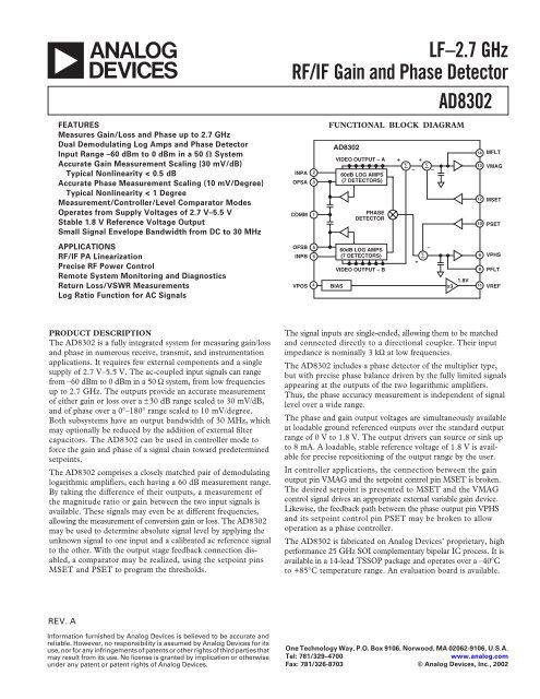
FUNCTIONAL BLOCK DIAGRAM<br />
<strong>AD8302</strong><br />
VIDEO OUTPUT – A<br />
60dB LOG AMPS<br />
(7 DETECTORS)<br />
PHASE<br />
DETECTOR<br />
60dB LOG AMPS<br />
(7 DETECTORS)<br />
VIDEO OUTPUT – B<br />
BIAS x3<br />
MFLT<br />
VMAG<br />
MSET<br />
PSET<br />
VPHS<br />
PFLT<br />
VREF<br />
The signal inputs are single-ended, allowing them to be matched<br />
<strong>and</strong> connected directly to a directional coupler. Their input<br />
impedance is nominally 3 kΩ at low frequencies.<br />
The <strong>AD8302</strong> includes a phase detector of the multiplier type,<br />
but with precise phase balance driven by the fully limited signals<br />
appearing at the outputs of the two logarithmic amplifiers.<br />
Thus, the phase accuracy measurement is independent of signal<br />
level over a wide range.<br />
The phase <strong>and</strong> gain output voltages are simultaneously available<br />
at loadable ground referenced outputs over the st<strong>and</strong>ard output<br />
range of 0 V to 1.8 V. The output drivers can source or sink up<br />
to 8 mA. A loadable, stable reference voltage of 1.8 V is available<br />
for precise repositioning of the output range by the user.<br />
In controller applications, the connection between the gain<br />
output pin VMAG <strong>and</strong> the setpoint control pin MSET is broken.<br />
The desired setpoint is presented to MSET <strong>and</strong> the VMAG<br />
control signal drives an appropriate external variable gain device.<br />
Likewise, the feedback path between the phase output pin VPHS<br />
<strong>and</strong> its setpoint control pin PSET may be broken to allow<br />
operation as a phase controller.<br />
The <strong>AD8302</strong> is fabricated on <strong>Analog</strong> <strong>Devices</strong>’ proprietary, high<br />
performance 25 <strong>GHz</strong> SOI complementary bipolar IC process. It is<br />
available in a 14-lead TSSOP package <strong>and</strong> operates over a –40°C<br />
to +85°C temperature range. An evaluation board is available.<br />
One Technology Way, P.O. Box 9106, Norwood, MA 02062-9106, U.S.A.<br />
Tel: 781/329–4700 www.analog.com<br />
Fax: 781/326-8703 © <strong>Analog</strong> <strong>Devices</strong>, Inc., 2002<br />
+<br />
–<br />
+<br />
+<br />
–<br />
–<br />
1.8V
<strong>AD8302</strong>–SPEC<strong>IF</strong>ICATIONS (T A = 25�C, V S = 5 V, VMAG shorted to MSET, VPHS shorted to PSET, 52.3 � shunt<br />
resistors connected to INPA <strong>and</strong> INPB, for <strong>Phase</strong> measurement P INPA = P INPB, unless otherwise noted.)<br />
Parameter<br />
OVERALL FUNCTION<br />
Conditions Min Typ Max Unit<br />
Input Frequency Range >0 2700 MHz<br />
<strong>Gain</strong> Measurement Range PIN at INPA, PIN at INPB = –30 dBm ± 30 dB<br />
<strong>Phase</strong> Measurement Range φIN at INPA > φIN at INPB ± 90 Degree<br />
Reference Voltage Output Pin VREF, –40°C ≤ TA ≤ +85°C 1.72 1.8 1.88 V<br />
INPUT INTE<strong>RF</strong>ACE Pins INPA <strong>and</strong> INPB<br />
Input Simplified Equivalent Circuit To AC Ground, f ≤ 500 MHz 3�2 kΩ�pF<br />
Input Voltage Range AC-Coupled (0 dBV = 1 V rms) –73 –13 dBV<br />
re: 50 Ω –60 0 dBm<br />
Center of Input Dynamic Range –43 dBV<br />
–30 dBm<br />
MAGNITUDE OUTPUT Pin VMAG<br />
Output Voltage Minimum 20 × Log (VINPA/VINPB) = –30 dB 30 mV<br />
Output Voltage Maximum 20 × Log (VINPA/VINPB) = +30 dB 1.8 V<br />
Center Point of Output (MCP) VINPA = VINPB 900 mV<br />
Output Current Source/Sink 8 mA<br />
Small Signal Envelope B<strong>and</strong>width Pin MFLT Open 30 MHz<br />
Slew Rate<br />
Response Time<br />
40 dB Change, Load 20 pF�10 kΩ 25 V/µs<br />
Rise Time Any 20 dB Change, 10%–90% 50 ns<br />
Fall Time Any 20 dB Change, 90%–10% 60 ns<br />
Settling Time Full-Scale 60 dB Change, to 1% Settling 300 ns<br />
PHASE OUTPUT Pin VPHS<br />
Output Voltage Minimum <strong>Phase</strong> Difference 180 Degrees 30 mV<br />
Output Voltage Maximum <strong>Phase</strong> Difference 0 Degrees 1.8 V<br />
<strong>Phase</strong> Center Point When φINPA = φINPB ±90° 900 mV<br />
Output Current Drive Source/Sink 8 mA<br />
Slew Rate 25 V/µs<br />
Small Signal Envelope B<strong>and</strong>width 30 MHz<br />
Response Time Any 15 Degree Change, 10%–90% 40 ns<br />
120 Degree Change CFILT = 1 pF, to 1% Settling 500 ns<br />
100 MHz MAGNITUDE OUTPUT<br />
Dynamic Range ± 1 dB Linearity PREF = –30 dBm (VREF = –43 dBV) 58 dB<br />
± 0.5 dB Linearity PREF = –30 dBm (VREF = –43 dBV) 55 dB<br />
± 0.2 dB Linearity PREF = –30 dBm (VREF = –43 dBV) 42 dB<br />
Slope From Linear Regression 29 mV/dB<br />
Deviation vs. Temperature Deviation from Output at 25°C<br />
–40°C ≤ TA ≤ +85°C, PINPA = PINPB = –30 dBm<br />
Deviation from Best Fit Curve at 25°C<br />
0.25 dB<br />
–40°C ≤ TA ≤ +85°C, PINPA = ±25 dB, PINPB = –30 dBm 0.25 dB<br />
<strong>Gain</strong> Measurement Balance PINPA = PINPB = –5 dBm to –50 dBm 0.2 dB<br />
PHASE OUTPUT<br />
Dynamic Range Less than ± 1 Degree Deviation from Best Fit Line 145 Degree<br />
Less than 10% Deviation in Instantaneous Slope 143 Degree<br />
Slope (Absolute Value) From Linear Regression about –90° or +90° 10 mV/Degree<br />
Deviation vs. Temperature Deviation from Output at 25°C<br />
–40°C ≤ T A ≤ +85°C, Delta <strong>Phase</strong> = 90 Degrees 0.7 Degree<br />
Deviation from Best Fit Curve at 25°C<br />
–40°C ≤ T A ≤ +85°C, Delta <strong>Phase</strong> = ±30 Degrees 0.7 Degree<br />
–2–<br />
REV. A
REV. A –3–<br />
<strong>AD8302</strong><br />
Parameter Conditions Min Typ Max Unit<br />
900 MHz MAGNITUDE OUTPUT<br />
Dynamic Range ± 1 dB Linearity PREF = –30 dBm (VREF = –43 dBV) 58 dB<br />
± 0.5 dB Linearity PREF = –30 dBm (VREF = –43 dBV) 54 dB<br />
± 0.2 dB Linearity PREF = –30 dBm (VREF = –43 dBV) 42 dB<br />
Slope From Linear Regression 28.7 mV/dB<br />
Deviation vs. Temperature Deviation from Output at 25°C<br />
–40°C ≤ TA ≤ +85°C, PINPA = PINPB = –30 dBm<br />
Deviation from Best Fit Curve at 25°C<br />
0.25 dB<br />
–40°C ≤ TA ≤ +85°C, PINPA = ±25 dB, PINPB = –30 dBm 0.25 dB<br />
<strong>Gain</strong> Measurement Balance PINPA = PINPB = –5 dBm to –50 dBm<br />
PHASE OUTPUT<br />
0.2 dB<br />
Dynamic Range Less than ± 1 Degree Deviation from Best Fit Line 143 Degree<br />
Less than 10% Deviation in Instantaneous Slope 143 Degree<br />
Slope (Absolute Value) From Linear Regression about –90° or +90° 10.1 mV/Degree<br />
Deviation Linear Deviation from Best Fit Curve at 25°C<br />
–40°C ≤ TA ≤ +85°C, Delta <strong>Phase</strong> = 90 Degrees 0.75 Degree<br />
–40°C ≤ TA ≤ +85°C, Delta <strong>Phase</strong> = ±30 Degrees 0.75 Degree<br />
<strong>Phase</strong> Measurement Balance <strong>Phase</strong> @ INPA = <strong>Phase</strong> @ INPB, PIN = –5 dBm to –50 dBm 0.8 Degree<br />
1900 MHz MAGNITUDE OUTPUT<br />
Dynamic Range ± 1 dB Linearity PREF = –30 dBm (VREF = –43 dBV) 57 dB<br />
± 0.5 dB Linearity PREF = –30 dBm (VREF = –43 dBV) 54 dB<br />
± 0.2 dB Linearity PREF = –30 dBm (VREF = –43 dBV) 42 dB<br />
Slope From Linear Regression 27.5 mV/dB<br />
Deviation vs. Temperature Deviation from Output at 25°C<br />
–40°C ≤ TA ≤ +85°C, PINPA = PINPB = –30 dBm<br />
Deviation from Best Fit Curve at 25°C<br />
0.27 dB<br />
–40°C ≤ TA ≤ +85°C, PINPA = ±25 dB, PINPB = –30 dBm 0.33 dB<br />
<strong>Gain</strong> Measurement Balance PINPA = PINPB = –5 dBm to –50 dBm<br />
PHASE OUTPUT<br />
0.2 dB<br />
Dynamic Range Less than ± 1 Degree Deviation from Best Fit Line 128 Degree<br />
Less than 10% Deviation in Instantaneous Slope 120 Degree<br />
Slope (Absolute Value) From Linear Regression about –90° or +90° 10.2 mV/Degree<br />
Deviation Linear Deviation from Best Fit Curve at 25°C<br />
–40°C ≤ TA ≤ +85°C, Delta <strong>Phase</strong> = 90 Degrees 0.8 Degree<br />
–40°C ≤ TA ≤ +85°C, Delta <strong>Phase</strong> = ±30 Degrees 0.8 Degree<br />
<strong>Phase</strong> Measurement Balance <strong>Phase</strong> @ INPA = <strong>Phase</strong> @ INPB, PIN = –5 dBm to –50 dBm 1 Degree<br />
2200 MHz MAGNITUDE OUTPUT<br />
Dynamic Range ± 1 dB Linearity PREF = –30 dBm (VREF = –43 dBV) 53 dB<br />
± 0.5 dB Linearity PREF = –30 dBm (VREF = –43 dBV) 51 dB<br />
± 0.2 dB Linearity PREF = –30 dBm (VREF = –43 dBV) 38 dB<br />
Slope From Linear Regression 27.5 mV/dB<br />
Deviation vs. Temperature Deviation from Output at 25°C<br />
–40°C ≤ TA ≤ +85°C, PINPA = PINPB = –30 dBm<br />
Deviation from Best Fit Curve at 25°C<br />
0.28 dB<br />
–40°C ≤ TA ≤ +85°C, PINPA = ±25 dB, PINPB = –30 dBm 0.4 dB<br />
<strong>Gain</strong> Measurement Balance PINPA = PINPB = –5 dBm to –50 dBm<br />
PHASE OUTPUT<br />
0.2 dB<br />
Dynamic Range Less than ± 1 Degree Deviation from Best Fit Line 115 Degree<br />
Less than 10% Deviation in Instantaneous Slope 110 Degree<br />
Slope (Absolute Value) From Linear Regression about –90° or +90° 10 mV/Degree<br />
Deviation Linear Deviation from Best Fit Curve at 25°C<br />
–40°C ≤ TA ≤ +85°C, Delta <strong>Phase</strong> = 90 Degrees 0.85 Degree<br />
–40°C ≤ TA ≤ +85°C, Delta <strong>Phase</strong> = ±30 Degrees 0.9 Degree<br />
REFERENCE VOLTAGE Pin VREF<br />
Output Voltage Load = 2 kΩ 1.7 1.8 1.9 V<br />
PSRR VS = 2.7 V to 5.5 V 0.25 mV/V<br />
Output Current Source/Sink (Less than 1% Change) 5 mA<br />
POWER SUPPLY Pin VPOS<br />
Supply 2.7 5.0 5.5 V<br />
Operating Current (Quiescent) VS = 5 V 19 25 mA<br />
–40°C ≤ TA ≤ +85°C 21 27 mA<br />
Specifications subject to change without notice.
<strong>AD8302</strong><br />
ABSOLUTE MAXIMUM RATINGS 1<br />
Supply Voltage V S . . . . . . . . . . . . . . . . . . . . . . . . . . . . . 5.5 V<br />
PSET, MSET Voltage . . . . . . . . . . . . . . . . . . . . . . VS + 0.3 V<br />
INPA, INPB Maximum Input . . . . . . . . . . . . . . . . . . –3 dBV<br />
Equivalent Power Re. 50 Ω . . . . . . . . . . . . . . . . . . 10 dBm<br />
θJA 2 . . . . . . . . . . . . . . . . . . . . . . . . . . . . . . . . . . . . . 150°C/W<br />
Maximum Junction Temperature . . . . . . . . . . . . . . . . 125°C<br />
Operating Temperature Range . . . . . . . . . . . –40°C to +85°C<br />
Storage Temperature Range . . . . . . . . . . . . –65°C to +150°C<br />
Lead Temperature Range (Soldering 60 sec) . . . . . . . . 300°C<br />
NOTES<br />
1 Stresses above those listed under Absolute Maximum Ratings may cause permanent<br />
damage to the device. This is a stress rating only; functional operation of the<br />
device at these or any other conditions above those indicated in the operational<br />
section of this specification is not implied. Exposure to absolute maximum rating<br />
conditions for extended periods may affect device reliability.<br />
2 JEDEC 1S St<strong>and</strong>ard (2-layer) board data.<br />
PIN FUNCTION DESCRIPTIONS<br />
–4–<br />
PIN CONFIGURATION<br />
COMM 1<br />
14 MFLT<br />
INPA 2<br />
13 VMAG<br />
OFSA 3 <strong>AD8302</strong> 12 MSET<br />
VPOS 4 TOP VIEW 11<br />
(Not to Scale)<br />
VREF<br />
OFSB 5<br />
10 PSET<br />
INPB 6<br />
9 VPHS<br />
COMM 7<br />
8 PFLT<br />
Pin No. Mnemonic Function<br />
Equivalent<br />
Circuit<br />
1, 7 COMM Device Common. Connect to low impedance ground.<br />
2 INPA High Input Impedance to Channel A. Must be ac-coupled. Circuit A<br />
3 OFSA A capacitor to ground at this pin sets the offset compensation filter corner<br />
<strong>and</strong> provides input decoupling.<br />
Circuit A<br />
4 VPOS Voltage Supply (VS), 2.7 V to 5.5 V<br />
5 OFSB A capacitor to ground at this pin sets the offset compensation filter corner<br />
<strong>and</strong> provides input decoupling.<br />
Circuit A<br />
6 INPB Input to Channel B. Same structure as INPA. Circuit A<br />
8 PFLT Low Pass Filter Terminal for the <strong>Phase</strong> Output Circuit E<br />
9 VPHS Single-Ended Output Proportional to the <strong>Phase</strong> Difference between INPA<br />
<strong>and</strong> INPB.<br />
Circuit B<br />
10 PSET Feedback Pin for Scaling of VPHS Output Voltage in Measurement Mode.<br />
Apply a setpoint voltage for controller mode.<br />
Circuit D<br />
11 VREF Internally Generated Reference Voltage (1.8 V Nominal) Circuit C<br />
12 MSET Feedback Pin for Scaling of VMAG Output Voltage Measurement Mode.<br />
Accepts a set point voltage in controller mode.<br />
Circuit D<br />
13 VMAG Single-Ended Output. Output voltage proportional to the decibel ratio<br />
of signals applied to INPA <strong>and</strong> INPB. Circuit B<br />
14 MFLT Low Pass Filter Terminal for the Magnitude Output Circuit E<br />
ORDERING GUIDE<br />
Package<br />
Model Temperature Range Package Description Option<br />
<strong>AD8302</strong>ARU –40°C to +85°C Tube, 14-Lead TSSOP RU-14<br />
<strong>AD8302</strong>ARU-REEL 13" Tape <strong>and</strong> Reel<br />
<strong>AD8302</strong>ARU-REEL7 7" Tape <strong>and</strong> Reel<br />
<strong>AD8302</strong>-EVAL Evaluation Board<br />
CAUTION<br />
ESD (electrostatic discharge) sensitive device. Electrostatic charges as high as 4000 V readily<br />
accumulate on the human body <strong>and</strong> test equipment <strong>and</strong> can discharge without detection. Although<br />
the <strong>AD8302</strong> features proprietary ESD protection circuitry, permanent damage may occur on<br />
devices subjected to high energy electrostatic discharges. Therefore, proper ESD precautions are<br />
recommended to avoid performance degradation or loss of functionality.<br />
WARNING!<br />
ESD SENSITIVE DEVICE<br />
REV. A
REV. A<br />
INPA(INPB)<br />
OFSA(OFSB)<br />
VPOS<br />
COMM<br />
10k�<br />
5k�<br />
Circuit C<br />
4k�<br />
100mV<br />
10pF<br />
VPOS<br />
4k�<br />
COMM<br />
Circuit A<br />
VREF<br />
+<br />
ON TO<br />
LOG-AMP<br />
–<br />
MSET<br />
(PSET)<br />
VPOS<br />
10k�<br />
10k�<br />
COMM<br />
Circuit D<br />
Figure 1. Equivalent Circuits<br />
–5–<br />
ACTIVE LOADS<br />
750�<br />
2k�<br />
VPOS<br />
CLASS A-B<br />
CONTROL<br />
COMM<br />
Circuit B<br />
25�<br />
VPOS<br />
COMM<br />
VMAG<br />
(VPHS)<br />
Circuit E<br />
<strong>AD8302</strong><br />
MFLT<br />
(PFLT)<br />
1.5pF
<strong>AD8302</strong>–Typical<br />
Performance Characteristics<br />
(V S = 5 V, V INPB is the reference input <strong>and</strong> V INPA is swept, unless otherwise noted. All references to dBm are referred to 50 �. For the phase output<br />
curves, the input signal levels are equal, unless otherwise noted.)<br />
VMAG – V<br />
2.0<br />
1.8<br />
1.6<br />
1.4<br />
1.2<br />
1.0<br />
0.8<br />
0.6<br />
0.4<br />
0.2<br />
100<br />
900<br />
2700<br />
2200<br />
1900<br />
0<br />
–30 –25 –20 –15 –10 –5 0 5 10 15 20 25 30<br />
MAGNITUDE RATIO – dB<br />
TPC 1. Magnitude Output (VMAG) vs. Input Level Ratio<br />
(<strong>Gain</strong>) V INPA/V INPB, Frequencies 100 MHz, 900 MHz,<br />
1900 MHz, 2200 MHz, 2700 MHz, 25�C, P INPB = –30 dBm,<br />
(Re: 50 Ω)<br />
VMAG – V<br />
2.0<br />
1.8<br />
1.6<br />
1.4<br />
1.2<br />
1.0<br />
0.8<br />
0.6<br />
0.4<br />
2700<br />
1900<br />
2200<br />
0.2<br />
0<br />
–30 –25 –20 –15 –10 –5 0 5 10<br />
900<br />
100<br />
15 20 25 30<br />
MAGNITUDE RATIO – dB<br />
TPC 2. VMAG vs. Input Level Ratio (<strong>Gain</strong>) V INPA/V INPB,<br />
Frequencies 100 MHz, 900 MHz, 1900 MHz, 2200 MHz,<br />
2700 MHz, P INPA = –30 dBm<br />
VMAG – V<br />
1.80<br />
1.65<br />
1.50<br />
1.35<br />
1.20<br />
1.05<br />
0.90<br />
0.75<br />
0.60<br />
0.45<br />
0.30<br />
0.15<br />
0<br />
–30<br />
–40�C<br />
+85�C<br />
+25�C<br />
–3.0<br />
–20 –10 0 10 20 30<br />
MAGNITUDE RATIO – dB<br />
TPC 3. VMAG Output <strong>and</strong> Log Conformance vs. Input<br />
Level Ratio (<strong>Gain</strong>), Frequency 100 MHz, –40�C, +25�C,<br />
<strong>and</strong> +85�C, Reference Level = –30 dBm<br />
3.0<br />
2.5<br />
2.0<br />
1.5<br />
1.0<br />
0.5<br />
0.0<br />
–0.5<br />
–1.0<br />
–1.5<br />
–2.0<br />
–2.5<br />
ERROR IN VMAG – dB<br />
–6–<br />
VMAG – V<br />
1.80<br />
1.65<br />
1.50<br />
1.35<br />
1.20<br />
1.05<br />
0.90<br />
0.75<br />
0.60<br />
0.45<br />
0.30<br />
0.15<br />
0<br />
–30<br />
–40�C<br />
+85�C<br />
+25�C<br />
–3.0<br />
–20 –10 0 10 20 30<br />
MAGNITUDE RATIO – dB<br />
3.0<br />
2.5<br />
2.0<br />
1.5<br />
1.0<br />
0.5<br />
0.0<br />
–0.5<br />
–1.0<br />
–1.5<br />
–2.0<br />
–2.5<br />
TPC 4. VMAG <strong>and</strong> Log Conformance vs. Input Level Ratio<br />
(<strong>Gain</strong>), Frequency 900 MHz, –40�C, +25�C, <strong>and</strong> +85�C,<br />
Reference Level = –30 dBm<br />
VMAG – V<br />
1.80<br />
1.65<br />
1.50<br />
1.35<br />
1.20<br />
1.05<br />
0.90<br />
0.75<br />
0.60<br />
0.45<br />
0.30<br />
0.15<br />
0<br />
–30<br />
–40�C<br />
+25�C<br />
+85�C<br />
–3.0<br />
–20 –10 0 10 20 30<br />
MAGNITUDE RATIO – dB<br />
3.0<br />
2.5<br />
2.0<br />
1.5<br />
1.0<br />
0.5<br />
0.0<br />
–0.5<br />
–1.0<br />
–1.5<br />
–2.0<br />
–2.5<br />
TPC 5. VMAG <strong>and</strong> Log Conformance vs. Input Level Ratio<br />
(<strong>Gain</strong>), Frequency 1900 MHz, –40�C, +25�C, <strong>and</strong> +85�C,<br />
Reference Level = –30 dBm<br />
VMAG – V<br />
1.80<br />
1.65<br />
1.50<br />
1.35<br />
1.20<br />
1.05<br />
0.90<br />
0.75<br />
0.60<br />
0.45<br />
0.30<br />
0.15<br />
0<br />
–30<br />
–40�C<br />
+25�C<br />
+85�C<br />
–3.0<br />
–20 –10 0 10 20 30<br />
MAGNITUDE RATIO – dB<br />
TPC 6. VMAG Output <strong>and</strong> Log Conformance vs. Input<br />
Level Ratio (<strong>Gain</strong>), Frequency 2200 MHz, –40�C, +25�C,<br />
<strong>and</strong> +85�C, Reference Level = –30 dBm<br />
3.0<br />
2.5<br />
2.0<br />
1.5<br />
1.0<br />
0.5<br />
0.0<br />
–0.5<br />
–1.0<br />
–1.5<br />
–2.0<br />
–2.5<br />
ERROR IN VMAG – dB<br />
ERROR IN VMAG – dB<br />
ERROR IN VMAG – dB<br />
REV. A
ERROR IN VMAG – dB<br />
1.5<br />
1.0<br />
0.5<br />
0.0<br />
–0.5<br />
–1.0<br />
–1.5<br />
–2.0<br />
–2.5<br />
REV. A<br />
3.0<br />
2.5<br />
2.0<br />
+85 C<br />
–40 C<br />
+85 C<br />
–40 C<br />
+25 C<br />
–3.0<br />
–30 –25 –20 –15 –10 –5 0 5 10 15 20 25 30<br />
MAGNITUDE RATIO – dB<br />
TPC 7. Distribution of Magnitude Error vs. Input Level<br />
Ratio (<strong>Gain</strong>), Three Sigma to Either Side of Mean,<br />
Frequency 900 MHz, –40�C, +25�C, <strong>and</strong> +85�C, Reference<br />
Level = –30 dBm<br />
ERROR IN VMAG – dB<br />
3.0<br />
2.5<br />
2.0<br />
1.5<br />
1.0<br />
0.5<br />
0.0<br />
–0.5<br />
–1.0<br />
–1.5<br />
–2.0<br />
–2.5<br />
+25 C<br />
–40 C<br />
–40 C<br />
+85 C<br />
+85 C<br />
–3.0<br />
–30 –25 –20 –15 –10 –5 0 5 10 15 20 25 30<br />
MAGNITUDE RATIO – dB<br />
TPC 8. Distribution of Error vs. Input Level Ratio (<strong>Gain</strong>),<br />
Three Sigma to Either Side of Mean, Frequency 1900 MHz,<br />
–40�C, +25�C, <strong>and</strong> +85�C, Reference Level = –30 dBm<br />
ERROR IN VMAG – dB<br />
3.0<br />
2.5<br />
2.0<br />
1.5<br />
1.0<br />
0.5<br />
0.0<br />
–0.5<br />
–1.0<br />
–1.5<br />
–2.0<br />
–2.5<br />
+25 C +85 C<br />
–40 C<br />
–40 C<br />
+85 C<br />
–3.0<br />
–30 –25 –20 –15 –10 –5 0 5 10 15 20 25 30<br />
MAGNITUDE RATIO – dB<br />
TPC 9. Distribution of Magnitude Error vs. Input Level<br />
Ratio (<strong>Gain</strong>), Three Sigma to Either Side of Mean,<br />
Frequency 2200 MHz, Temperatures –40�C, +25�C, <strong>and</strong><br />
+85�C, Reference Level = –30 dBm<br />
–7–<br />
VMAG – V<br />
2.0<br />
1.8<br />
1.6<br />
1.4<br />
1.2<br />
1.0<br />
0.8<br />
0.6<br />
0.4<br />
0.2<br />
<strong>AD8302</strong><br />
0.0<br />
–30 –25 –20 –15 –10 –5 0 5 10 15 20 25 30<br />
MAGNITUDE RATIO – dB<br />
TPC 10. Distribution of VMAG vs. Input Level Ratio (<strong>Gain</strong>),<br />
Three Sigma to Either Side of Mean, Frequency 1900 MHz,<br />
Temperatures Between –40�C <strong>and</strong> +85�C, Reference Level<br />
= –30 dBm<br />
VMAG – V<br />
1.8<br />
1.6<br />
1.4<br />
1.2<br />
1.0<br />
0.8<br />
0.6<br />
0.4<br />
0.2<br />
0.0<br />
–30<br />
–30dBm –15dBm<br />
–45dBm<br />
–45dBm<br />
–15dBm<br />
–30dBm<br />
3.0<br />
2.5<br />
1.5<br />
1.0<br />
0.5<br />
0.0<br />
–0.5<br />
–1.0<br />
–1.5<br />
–3.0<br />
–20 –10 0 10 20 30<br />
MAGNITUDE RATIO – dB<br />
2.0<br />
–2.0<br />
–2.5<br />
TPC 11. VMAG Output <strong>and</strong> Log Conformance vs. Input<br />
Level Ratio (<strong>Gain</strong>), Reference Level = –15 dBm, –30 dBm,<br />
<strong>and</strong> –45 dBm, Frequency 1900 MHz<br />
VMAG – V<br />
1.10<br />
1.05<br />
1.00<br />
0.95<br />
0.90<br />
0.85<br />
0.80<br />
P INPA = P INPB + 5dB<br />
P INPA = P INPB<br />
P INPA = P INPB – 5dB<br />
0.75<br />
–65 –60 –55 –50 –45 –40 –35 –30 –25 –20 –15 –10<br />
INPUT LEVEL – dBm<br />
–5 0<br />
TPC 12. VMAG Output vs. Input Level for P INPA = P INPB,<br />
PINPA = PINPB + 5 dB, PINPA = PINPB – 5 dB, Frequency 1900 MHz<br />
ERROR IN VMAG – dB
<strong>AD8302</strong><br />
VMAG – V<br />
1.06<br />
1.04<br />
1.02<br />
1.00<br />
0.98<br />
0.96<br />
0.94<br />
0.92<br />
0.90<br />
0.88<br />
0.86<br />
0.84<br />
0.82<br />
0.80<br />
0.78<br />
0.76<br />
0.74<br />
0<br />
P INPA = P INPB + 5dB<br />
P INPA = P INPB<br />
P INPA = P INPB – 5dB<br />
200 400 600 800 1000 1200 1400 1600 1800 2000 2200<br />
FREQUENCY – MHz<br />
TPC 13. VMAG Output vs. Frequency, for P INPA = P INPB, P INPA<br />
= P INPB + 5 dB, <strong>and</strong> P INPA = P INPB – 5 dB, P INPB = –30 dBm<br />
CHANGE IN SLOPE – mV<br />
0.4<br />
0.2<br />
0<br />
–0.2<br />
–0.4<br />
–0.6<br />
–0.8<br />
–1.0<br />
–1.2<br />
–1.4<br />
–1.6<br />
–1.8<br />
–40 –20 0 20 40 60 80<br />
TEMPERATURE – �C<br />
TPC 14. Change in VMAG Slope vs. Temperature, Three<br />
Sigma to Either Side of Mean, Frequencies 1900 MHz<br />
VMAG – mV<br />
25<br />
20<br />
15<br />
10<br />
5<br />
0<br />
–5<br />
–10<br />
–15<br />
–20<br />
–25<br />
–40 –30 –20 –10 0 10 20 30 40 50 60<br />
TEMPERATURE – �C<br />
85<br />
70 80 90<br />
TPC 15. Change in Center Point of Magnitude Output<br />
(MCP) vs. Temperature, Three Sigma to Either Side of<br />
Mean, Frequencies 1900 MHz<br />
–8–<br />
PERCENT<br />
18<br />
15<br />
12<br />
9<br />
6<br />
3<br />
0<br />
0.80 0.85 0.90<br />
MCP – V<br />
0.95<br />
1.00<br />
TPC 16. Center Point of Magnitude Output (MCP)<br />
Distribution Frequencies 900 MHz, 17,000 Units<br />
PERCENT<br />
18<br />
15<br />
12<br />
9<br />
6<br />
3<br />
0<br />
27.0 27.5 28.0 28.5<br />
29.0<br />
VMAG SLOPE – mV/dB<br />
29.5 30.0<br />
TPC 17. VMAG Slope, Frequency 900 MHz, 17,000 Units<br />
SLOPE OF VMAG – V<br />
0.032<br />
0.030<br />
0.028<br />
0.026<br />
0.024<br />
0<br />
200<br />
400<br />
600<br />
800<br />
1000<br />
1200<br />
1400<br />
1600<br />
1800<br />
FREQUENCY – MHz<br />
2000<br />
2200<br />
2400<br />
TPC 18. VMAG Slope vs. Frequency<br />
2600<br />
2800<br />
REV. A
REV. A<br />
25ns<br />
HORIZONTAL<br />
20mV PER<br />
VERTICAL<br />
DIVISION<br />
TPC 19. Magnitude Output Response to 4 dB Step, for<br />
P INPB = –30 dBm, P INPA = –32 dBm to –28 dBm, Frequency<br />
1900 MHz, No Filter Capacitor<br />
20mV PER<br />
VERTICAL<br />
DIVISION<br />
1.00�s<br />
HORIZONTAL<br />
TPC 20. Magnitude Output Response to 4 dB Step, for<br />
P INPB = –30 dBm, P INPA = –32 dBm to –28 dBm, Frequency<br />
1900 MHz, 1 nF Filter Capacitor<br />
200mV PER<br />
VERTICAL<br />
DIVISION<br />
100ns<br />
HORIZONTAL<br />
TPC 21. Magnitude Output Response to 40 dB Step, for<br />
PINPB = –30 dBm, PINPA = –50 dBm to –10 dBm, Supply 5 V,<br />
Frequency 1900 MHz, No Filter Capacitor<br />
–9–<br />
VMAG – nV/ Hz<br />
VMAG – nV/ Hz<br />
10000<br />
1000<br />
100<br />
10000<br />
10<br />
1k 10k<br />
1000<br />
100<br />
INPUT –50dBm<br />
INPUT –30dBm<br />
INPUT –10dBm<br />
<strong>AD8302</strong><br />
100k 1M 10M 100M<br />
FREQUENCY – Hz<br />
TPC 22. Magnitude Output Noise Spectral<br />
Density, P INPA = P INPB = –10 dBm, –30 dBm,<br />
–50 dBm, No Filter Capacitor<br />
10<br />
1k 10k<br />
INPUT –50dBm<br />
INPUT –30dBm<br />
INPUT –10dBm<br />
100k 1M 10M 100M<br />
FREQUENCY – Hz<br />
TPC 23. Magnitude Output Noise Spectral Density, PINPA = PINPB<br />
= –10 dBm, –30 dBm, –50 dBm, with Filter Capacitor, C = 1 nF<br />
VMAG (PEAK-TO-PEAK) – V<br />
0.18<br />
0.16<br />
0.14<br />
0.12<br />
0.10<br />
0.08<br />
0.06<br />
0.04<br />
0.02<br />
1900<br />
100<br />
0.00<br />
–25 –20<br />
900<br />
2700<br />
2200<br />
–15 –10 –5 0 5 10 15 20 25<br />
MAGNITUDE RATIO – dB<br />
TPC 24. VMAG Peak-to-Peak Output Induced by Sweeping<br />
<strong>Phase</strong> Difference through 360 Degrees vs. Magnitude Ratio,<br />
Frequencies 100 MHz, 900 MHz, 1900 MHz, 2200 MHz, <strong>and</strong><br />
2700 MHz
<strong>AD8302</strong><br />
PHASE OUT – V<br />
1.8<br />
1.6<br />
1.4<br />
1.2<br />
1.0<br />
0.8<br />
0.6<br />
0.4<br />
0.2<br />
0.0<br />
–180 –140<br />
100MHz<br />
900MHz<br />
1900MHz<br />
2200MHz<br />
2700MHz<br />
–100 –60 –20 20 60 100 140 180<br />
PHASE D<strong>IF</strong>FERENCE – Degrees<br />
TPC 25. <strong>Phase</strong> Output (VPHS) vs. Input <strong>Phase</strong> Difference,<br />
Input Levels –30 dBm, Frequencies 100 MHz, 900 MHz,<br />
1900 MHz, 2200 MHz, Supply 5 V, 2700 MHz<br />
PHASE OUT – V<br />
1.80<br />
1.62<br />
1.44<br />
1.26<br />
1.08<br />
0.90<br />
0.72<br />
0.54<br />
0.36<br />
0.18<br />
0.00<br />
–180 –150 –120 –90 –60 –30 0 30 60 90<br />
PHASE D<strong>IF</strong>FERENCE – Degrees<br />
10<br />
8<br />
6<br />
4<br />
2<br />
0<br />
–2<br />
–4<br />
–6<br />
–8<br />
ERROR – Degrees<br />
120 150<br />
–10<br />
180<br />
TPC 26. VPHS Output <strong>and</strong> Nonlinearity vs. Input <strong>Phase</strong><br />
Difference, Input Levels –30 dBm, Frequency 100 MHz<br />
PHASE OUT – V<br />
1.80<br />
1.62<br />
1.44<br />
1.26<br />
1.08<br />
0.90<br />
0.72<br />
0.54<br />
0.36<br />
0.18<br />
0.00<br />
–180 –150 –120 –90 –60 –30 0 30 60 90<br />
PHASE D<strong>IF</strong>FERENCE – Degrees<br />
10<br />
8<br />
6<br />
4<br />
2<br />
0<br />
–2<br />
–4<br />
–6<br />
–8<br />
ERROR – Degrees<br />
120 150<br />
–10<br />
180<br />
TPC 27. VPHS Output <strong>and</strong> Nonlinearity vs. Input <strong>Phase</strong><br />
Difference, Input Levels –30 dBm, Frequency 900 MHz<br />
–10–<br />
PHASE OUT – V<br />
1.80<br />
1.62<br />
1.44<br />
1.26<br />
1.08<br />
0.90<br />
0.72<br />
0.54<br />
0.36<br />
0.18<br />
0.00<br />
–180 –150 –120 –90 –60 –30 0 30 60 90<br />
PHASE D<strong>IF</strong>FERENCE – Degrees<br />
10<br />
8<br />
6<br />
4<br />
2<br />
0<br />
–2<br />
–4<br />
–6<br />
–8<br />
ERROR – Degrees<br />
120 150<br />
–10<br />
180<br />
TPC 28. VPHS Output <strong>and</strong> Nonlinearity vs. Input <strong>Phase</strong><br />
Difference, Input Levels –30 dBm, Frequency 1900 MHz<br />
PHASE OUT – V<br />
1.80<br />
1.62<br />
1.44<br />
1.26<br />
1.08<br />
0.90<br />
0.72<br />
0.54<br />
0.36<br />
0.18<br />
0.00<br />
–180 –150 –120 –90 –60 –30 0 30 60 90<br />
PHASE D<strong>IF</strong>FERENCE – Degrees<br />
10<br />
8<br />
6<br />
4<br />
2<br />
0<br />
–2<br />
–4<br />
–6<br />
–8<br />
ERROR – Degrees<br />
120 150<br />
–10<br />
180<br />
TPC 29. VPHS Output <strong>and</strong> Nonlinearity vs. Input <strong>Phase</strong><br />
Difference, Input Levels –30 dBm, Frequency 2200 MHz<br />
ERROR – Degrees<br />
10<br />
8<br />
6<br />
4<br />
2<br />
0<br />
–2<br />
–4<br />
–6<br />
–8<br />
+85�C<br />
+25�C<br />
–40�C<br />
–10<br />
–180 –150 –120 –90 –60 –30 0 30 60 90<br />
PHASE D<strong>IF</strong>FERENCE – Degrees<br />
120 150 180<br />
TPC 30. Distribution of VPHS Error vs. Input <strong>Phase</strong> Difference,<br />
Three Sigma to Either Side of Mean, Frequency<br />
900 MHz, –40�C, +25�C, <strong>and</strong> +85�C, Input Levels –30 dBm<br />
REV. A
ERROR – Degrees<br />
REV. A<br />
10<br />
8<br />
6<br />
4<br />
2<br />
0<br />
–2<br />
–4<br />
–6<br />
–8<br />
+85�C<br />
+25�C<br />
–40�C<br />
–10<br />
–180 –150 –120 –90 –60 –30 0 30 60 90<br />
PHASE D<strong>IF</strong>FERENCE – Degrees<br />
120 150 180<br />
TPC 31. Distribution of VPHS Error vs. Input <strong>Phase</strong><br />
Difference, Three Sigma to Either Side of Mean, Frequency<br />
1900 MHz, –40�C, +25�C, <strong>and</strong> +85�C, Supply 5 V, Input<br />
Levels P INPA = P INPB = –30 dBm<br />
ERROR – Degrees<br />
10<br />
8<br />
6<br />
4<br />
2<br />
0<br />
–2<br />
–4<br />
–6<br />
–8<br />
–40�C<br />
+85�C +25�C<br />
–10<br />
–180 –150 –120 –90 –60 –30 0 30 60 90<br />
PHASE D<strong>IF</strong>FERENCE – Degrees<br />
120 150 180<br />
TPC 32. Distribution of VPHS Error vs. Input <strong>Phase</strong> Difference,<br />
Three Sigma to Either Side of Mean, Frequency<br />
2200 MHz, –40�C, +25�C, <strong>and</strong> +85�C, Input Levels –30 dBm<br />
VPHS – V<br />
1.8<br />
1.6<br />
1.4<br />
1.2<br />
1.0<br />
0.8<br />
0.6<br />
0.4<br />
0.2<br />
0.0<br />
–180 –150 –120 –90 –60 –30 0 30 60 90<br />
PHASE D<strong>IF</strong>FERENCE – Degrees<br />
120 150 180<br />
TPC 33. Distribution of VPHS vs. Input <strong>Phase</strong> Difference,<br />
Three Sigma to Either Side of Mean, Frequency<br />
900 MHz, Temperature between –40�C <strong>and</strong> +85�C, Input<br />
Levels –30 dBm<br />
–11–<br />
CHANGE IN VPHS SLOPE – mV<br />
0.15<br />
0.10<br />
0.05<br />
0.00<br />
–0.05<br />
–0.10<br />
–0.15<br />
–0.20<br />
–0.25<br />
–0.30<br />
MEAN +3 SIGMA<br />
MEAN –3 SIGMA<br />
–0.35<br />
–40 –30 –20 –10 0 10 20 30 40 50<br />
TEMPERATURE – �C<br />
<strong>AD8302</strong><br />
60 70 80 90<br />
TPC 34. Change in VPHS Slope vs. Temperature, Three<br />
Sigma to Either Side of Mean, Frequency 1900 MHz<br />
PERCENT<br />
10<br />
5<br />
0<br />
–5<br />
–10<br />
–15<br />
–20<br />
–25<br />
–30<br />
–35<br />
+3 SIGMA<br />
–3 SIGMA<br />
–40<br />
–40 –30 –20 –10 0 10 20 30 40 50<br />
VPHS – mV/Degree<br />
60 70 80 90<br />
TPC 35. Change in <strong>Phase</strong> Center Point (PCP) vs.<br />
Temperature, Three Sigma to Either Side of Mean,<br />
Frequency 1900 MHz<br />
PERCENT<br />
18<br />
15<br />
12<br />
9<br />
6<br />
3<br />
0<br />
0.75 0.80 0.85 0.90<br />
PCP – V<br />
0.95<br />
1.00 1.05<br />
TPC 36. <strong>Phase</strong> Center Point (PCP) Distribution, Frequency<br />
900 MHz, 17,000 Units
<strong>AD8302</strong><br />
PERCENT<br />
16<br />
14<br />
12<br />
10<br />
8<br />
6<br />
4<br />
2<br />
0<br />
9.5 9.7 9.9 10.1 10.3 10.5 10.7 10.9<br />
VPHS – mV/Degree<br />
11.1<br />
TPC 37. VPHS Slope Distribution, Frequency<br />
900 MHz<br />
10mV PER<br />
VERTICAL<br />
DIVISION<br />
50ns HORIZONTAL<br />
TPC 38. VPHS Output Response to 4� Step with Nominal<br />
<strong>Phase</strong> Shift of 90�, Input Levels –30 dBm, Frequency<br />
1900 MHz, 25�C, 1 pF Filter Capacitor<br />
10mV PER<br />
VERTICAL<br />
DIVISION<br />
2�s HORIZONTAL<br />
TPC 39. VPHS Output Response to 4� Step with Nominal<br />
<strong>Phase</strong> Shift of 90�, Input Levels P INPA = P INPB = –30 dBm,<br />
Supply 5 V, Frequency 1900 MHz, 25�C, with 100 pF Filter<br />
Capacitor<br />
–12–<br />
100mV PER<br />
VERTICAL<br />
DIVISION<br />
50ns HORIZONTAL<br />
TPC 40. VPHS Output Response to 40� Step with Nominal<br />
<strong>Phase</strong> Shift of 90�, Input Levels P INPA = P INPB = –30 dBm,<br />
Frequency 1900 MHz,1 pF Filter Capacitor<br />
VPHS – nV/ Hz<br />
10000<br />
1000<br />
100<br />
10<br />
1k<br />
INPUT –50dBm<br />
INPUT –30dBm<br />
INPUT –10dBm<br />
10k 100k 1M 10M 100M<br />
FREQUENCY – Hz<br />
TPC 41. VPHS Output Noise Spectral Density vs. Frequency,<br />
P INPA = –30 dBm, P INPB = –10 dBm, –30 dBm, –50 dBm, <strong>and</strong><br />
90� Input <strong>Phase</strong> Difference<br />
PHASE OUT – V<br />
1.80<br />
1.62<br />
1.44<br />
1.26<br />
1.08<br />
0.90<br />
0.72<br />
0.54<br />
0.36<br />
0.18<br />
P INPA = –45dBm<br />
P INPA = –30dBm<br />
0.00<br />
–180 –150 –120 –90 –60 –30 0 30 60 90<br />
PHASE D<strong>IF</strong>FERENCE – Degrees<br />
P INPA = –15dBm<br />
120 150 180<br />
TPC 42. <strong>Phase</strong> Output vs. Input <strong>Phase</strong> Difference, PINPA =<br />
P INPB, P INPA = P INPB + 15 dB, P INPA = P INPB – 15 dB, Frequency<br />
900 MHz<br />
REV. A
REV. A<br />
ABSOLUTE VALUE OF VPHS<br />
INSTANTANEOUS SLOPE – mV<br />
12<br />
10<br />
8<br />
6<br />
4<br />
2<br />
P INPA = –15dBm<br />
P INPA = –45dBm<br />
P INPA = –30dBm<br />
0<br />
–180 –150 –120 –90 –60 –30 0 30 60 90<br />
PHASE D<strong>IF</strong>FERENCE – Degrees<br />
120 150 180<br />
TPC 43. <strong>Phase</strong> Output Instantaneous Slope,<br />
P INPA = P INPB, P INPA = P INPB + 15 dB, P INPA = P INPB – 15 dB,<br />
Frequency 900 MHz<br />
PHASE OUT – V<br />
1.80<br />
1.62<br />
1.44<br />
1.26<br />
1.08<br />
0.90<br />
0.72<br />
0.54<br />
0.36<br />
0.18<br />
P INPA = –20dBm<br />
P INPA = –40dBm<br />
P INPA = –30dBm<br />
0.00<br />
–180 –150 –120 –90 –60 –30 0 30 60 90<br />
PHASE D<strong>IF</strong>FERENCE – Degrees<br />
120 150 180<br />
TPC 44. <strong>Phase</strong> Output vs. Input <strong>Phase</strong> Difference,<br />
P INPA = P INPB, P INPA = P INPB + 10 dB, P INPA = P INPB – 10 dB,<br />
Frequency 1900 MHz, Supply 5 V<br />
ABSOLUTE VALUE OF VPHS<br />
INSTANTANEOUS SLOPE – mV<br />
12<br />
10<br />
8<br />
6<br />
4<br />
2<br />
P INPA = –30dBm<br />
P INPA = –40dBm<br />
PINPA = –20dBm<br />
0<br />
–180 –150 –120 –90 –60 –30 0 30 60 90<br />
PHASE D<strong>IF</strong>FERENCE – Degrees<br />
120 150 180<br />
TPC 45. <strong>Phase</strong> Output Instantaneous Slope, P INPA =<br />
PINPB, PINPA = PINPB + 10 dB, PINPA = PINPB – 10 dB,<br />
Frequency 1900 MHz, Supply 5 V<br />
–13–<br />
PHASE OUT – V<br />
1.80<br />
1.62<br />
1.44<br />
1.26<br />
1.08<br />
0.90<br />
0.72<br />
0.54<br />
0.36<br />
P INPA = –20dBm<br />
P INPA = –40dBm<br />
0.18<br />
PINPA = –30dBm<br />
0.00<br />
–180 –150 –120 –90 –60 –30 0 30 60 90<br />
PHASE D<strong>IF</strong>FERENCE – Degrees<br />
<strong>AD8302</strong><br />
120 150 180<br />
TPC 46. <strong>Phase</strong> Output vs. Input <strong>Phase</strong> Difference,<br />
P INPA = P INPB, P INPA = P INPB + 10 dB, P INPA = P INPB – 10 dB,<br />
Frequency 2200 MHz<br />
ABSOLUTE VALUE OF VPHS<br />
INSTANTANEOUS SLOPE – mV<br />
12<br />
10<br />
8<br />
6<br />
4<br />
2<br />
P INPA = –30dBm<br />
P INPA = –20dBm<br />
P INPA = –40dBm<br />
0<br />
–180 –150 –120 –90 –60 –30 0 30 60 90 120 150 180<br />
PHASE D<strong>IF</strong>FERENCE – Degrees<br />
TPC 47. <strong>Phase</strong> Output Instantaneous Slope, P INPA = P INPB,<br />
P INPA = P INPB + 10 dB, P INPA = P INPB – 10 dB, Frequency<br />
2200 MHz<br />
RESISTANCE – �<br />
4000<br />
3500<br />
3000<br />
2500<br />
2000<br />
1500<br />
1000<br />
500<br />
0<br />
0<br />
REAL SHUNT Z (�)<br />
SHUNT C<br />
SHUNT R<br />
CAPACITANCE SHUNT Z (pF)<br />
500 1000 1500 2000 2500<br />
FREQUENCY – MHz<br />
TPC 48. Input Impedance, Modeled as Shunt R in Parallel<br />
with Shunt C<br />
4.0<br />
3.5<br />
3.0<br />
2.5<br />
2.0<br />
1.5<br />
1.0<br />
0.5<br />
0.0<br />
CAPACITANCE – pF
<strong>AD8302</strong><br />
VREF – mV<br />
8<br />
6<br />
4<br />
2<br />
0<br />
–2<br />
–4<br />
–6<br />
–40 –30 –20 –10 0 10 20 30 40 50 60 70 80 90<br />
TEMPERATURE – �C<br />
TPC 49. Change in VREF vs. Temperature, Three Sigma to<br />
Either Side of Mean<br />
NOISE – nV/ Hz<br />
120<br />
100<br />
80<br />
60<br />
40<br />
20<br />
0<br />
1k<br />
10k 100k 1M 10M 100M<br />
FREQUENCY – Hz<br />
TPC 50. VREF Output Noise Spectral Density vs.<br />
Frequency<br />
–14–<br />
PERCENT<br />
18<br />
15<br />
12<br />
9<br />
6<br />
3<br />
0<br />
1.74<br />
1.76 1.78 1.80 1.82 1.84 1.86 1.88<br />
VREF – V<br />
TPC 51. VREF Distribution, 17,000 Units<br />
REV. A
GENERAL DESCRIPTION AND THEORY<br />
The <strong>AD8302</strong> measures the magnitude ratio, defined here as<br />
gain, <strong>and</strong> phase difference between two signals. A pair of<br />
matched logarithmic amplifiers provide the measurement, <strong>and</strong><br />
their hard-limited outputs drive the phase detector.<br />
Basic Theory<br />
Logarithmic amplifiers (log amps) provide a logarithmic compression<br />
function that converts a large range of input signal<br />
levels to a compact decibel-scaled output. The general mathematical<br />
form is:<br />
REV. A<br />
V V log V / V<br />
(1)<br />
= ( )<br />
OUT SLP IN Z<br />
where VIN is the input voltage, VZ is called the intercept (voltage),<br />
<strong>and</strong> VSLP is called the slope (voltage). It is assumed throughout<br />
that log(x) represents the log10(x) function. VSLP is thus the<br />
volts/decade, <strong>and</strong> since a decade of voltage corresponds to<br />
20 dB, VSLP/20 is the volts/dB. VZ is the value of input<br />
signal that results in an output of zero <strong>and</strong> need not correspond<br />
to a physically realizable part of the log amp signal range.<br />
While the slope is fundamentally a characteristic of the log amp,<br />
the intercept is a function of the input waveform as well. 1<br />
Furthermore, the intercept is typically more sensitive to temperature<br />
<strong>and</strong> frequency than the slope. When single log amps<br />
are used for power measurement, this variability introduces<br />
errors into the absolute accuracy of the measurement since the<br />
intercept represents a reference level.<br />
The <strong>AD8302</strong> takes the difference in the output of two identical<br />
log amps, each driven by signals of similar waveforms but at<br />
different levels. Since subtraction in the logarithmic domain<br />
corresponds to a ratio in the linear domain, the resulting<br />
output becomes:<br />
V V log V / V<br />
(2)<br />
= ( )<br />
MAG SLP INA INB<br />
where VINA <strong>and</strong> VINB are the input voltages, VMAG is the output<br />
corresponding to the magnitude of the signal level difference,<br />
<strong>and</strong> VSLP is the slope. Note that the intercept, VZ, has dropped<br />
out. Unlike the measurement of power, when measuring a dimensionless<br />
quantity such as relative signal level, no independent<br />
reference or intercept need be invoked. In essence, one signal<br />
serves as the intercept for the other. Variations in intercept due<br />
to frequency, process, temperature, <strong>and</strong> supply voltage affect both<br />
channels identically <strong>and</strong> hence do not affect the difference. This<br />
technique depends on the two log amps being well matched<br />
in slope <strong>and</strong> intercept to ensure cancellation. This is the case<br />
for an integrated pair of log amps. Note that if the two signals<br />
have different waveforms (e.g., different peak-to-average ratios)<br />
or different frequencies, an intercept difference may appear, introducing<br />
a systematic offset.<br />
The log amp structure consists of a cascade of linear/limiting<br />
gain stages with demodulating detectors. Further details about<br />
the structure <strong>and</strong> function of log amps can be found in data<br />
sheets for other log amps produced by <strong>Analog</strong> <strong>Devices</strong>. 2 The<br />
output of the final stage of a log amp is a fully limited signal<br />
over most of the input dynamic range. The limited outputs from<br />
both log amps drive an exclusive-OR style digital phase detector.<br />
Operating strictly on the relative zero-crossings of the limited signals,<br />
the extracted phase difference is independent of the original<br />
input signal levels. The phase output has the general form:<br />
NOTES<br />
1See the data sheet for the AD640 for a description of the effect of waveform on<br />
the intercept of log amps.<br />
2For example, see the data sheet for the AD8307.<br />
–15–<br />
[ ]<br />
<strong>AD8302</strong><br />
V V ΦV Φ V<br />
(3)<br />
= ( )− ( )<br />
PHS Φ INA INB<br />
where VΦ is the phase slope in mV/degree <strong>and</strong> Φ is each signal’s<br />
relative phase in degrees.<br />
Structure<br />
The general form of the <strong>AD8302</strong> is shown in Figure 2. The<br />
major blocks consist of two demodulating log amps, a phase<br />
detector, output amplifiers, a biasing cell, <strong>and</strong> an output reference<br />
voltage buffer. The log amps <strong>and</strong> phase detector process<br />
the high frequency signals <strong>and</strong> deliver the gain <strong>and</strong> phase information<br />
in current form to the output amplifiers. The output<br />
amplifiers determine the final gain <strong>and</strong> phase scaling. External<br />
filter capacitors set the averaging time constants for the respective<br />
outputs. The reference buffer provides a 1.80 V reference<br />
voltage that tracks the internal scaling constants.<br />
INPA<br />
OFSA<br />
COMM<br />
OFSB<br />
INPB<br />
VPOS<br />
VIDEO OUTPUT – A<br />
60dB LOG AMPS<br />
(7 DETECTORS)<br />
PHASE<br />
DETECTOR<br />
60dB LOG AMPS<br />
(7 DETECTORS)<br />
VIDEO OUTPUT – B<br />
+<br />
BIAS x3 1.8V<br />
–<br />
+<br />
+<br />
–<br />
–<br />
MFLT<br />
VMAG<br />
MSET<br />
PSET<br />
VPHS<br />
PFLT<br />
VREF<br />
Figure 2. General Structure<br />
Each log amp consists of a cascade of six 10 dB gain stages with<br />
seven associated detectors. The individual gain stages have 3 dB<br />
b<strong>and</strong>widths in excess of 5 <strong>GHz</strong>. The signal path is fully differential<br />
to minimize the effect of common-mode signals <strong>and</strong> noise.<br />
Since there is a total of 60 dB of cascaded gain, slight dc offsets<br />
can cause limiting of the latter stages, which may cause measurement<br />
errors for small signals. This is corrected by a feedback<br />
loop. The nominal high-pass corner frequency, fHP, of this loop<br />
is set internally at 200 MHz but can be lowered by adding external<br />
capacitance to the OFSA <strong>and</strong> OFSB pins. Signals at frequencies<br />
well below the high-pass corner are indistinguishable from dc<br />
offsets <strong>and</strong> are also nulled. The difference in the log amp outputs<br />
is performed in the current domain, yielding by analogy to<br />
Equation 2:<br />
I I log V / V<br />
(4)<br />
= ( )<br />
LA SLP INA INB<br />
where ILA <strong>and</strong> ISLP are the output current difference <strong>and</strong> the<br />
characteristic slope (current) of the log amps, respectively. The<br />
slope is derived from an accurate reference designed to be insensitive<br />
to temperature <strong>and</strong> supply voltage.<br />
The phase detector uses a fully symmetric structure with respect<br />
to its two inputs to maintain balanced delays along both signal<br />
paths. Fully differential signaling again minimizes the sensitivity<br />
to common-mode perturbations. The current-mode equivalent<br />
to Equation 3 is:<br />
[ ]<br />
I = I Φ( V )− Φ( V )− 90 °<br />
(5)<br />
PD Φ INA INB<br />
where I PD <strong>and</strong> I Φ are the output current <strong>and</strong> characteristic slope<br />
associated with the phase detector, respectively. The slope is<br />
derived from the same reference as the log amp slope.
<strong>AD8302</strong><br />
Note that by convention, the phase difference is taken in the range<br />
from –180° to +180°. Since this style of phase detector does not<br />
distinguish between ±90°, it is considered to have an unambiguous<br />
180° phase difference range that can be either 0° to +180° centered<br />
at +90° or 0° to –180° centered at –90°.<br />
The basic structure of both output interfaces is shown in Figure 3. It<br />
accepts a setpoint input <strong>and</strong> includes an internal integrating/averaging<br />
capacitor <strong>and</strong> a buffer amplifier with gain K. External access to<br />
these setpoints provides for several modes of operation <strong>and</strong> enables<br />
flexible tailoring of the gain <strong>and</strong> phase transfer characteristics. The<br />
setpoint interface block, characterized by a transresistance <strong>RF</strong>, generates<br />
a current proportional to the voltage presented to its input pin,<br />
MSET or PSET. A precise offset voltage of 900 mV is introduced<br />
internally to establish the center-point (VCP) for the gain <strong>and</strong> phase<br />
functions, i.e., the setpoint voltage that corresponds to a gain of 0 dB<br />
<strong>and</strong> a phase difference of 90°. This setpoint current is subtracted<br />
from the signal current, IIN, coming from the log amps in the gain<br />
channel or from the phase detector in the phase channel. The resulting<br />
difference is integrated on the averaging capacitors at either pin<br />
MFLT or PFLT <strong>and</strong> then buffered by the output amplifier to the<br />
respective output pins, VMAG <strong>and</strong> VPHS. With this open-loop<br />
arrangement, the output voltage is a simple integration of the difference<br />
between the measured gain/phase <strong>and</strong> the desired setpoint:<br />
( ) ( )<br />
V = R I −I<br />
/ sT<br />
(6)<br />
OUT F IN FB<br />
where <strong>IF</strong>B is the feedback current equal to (VSET – VCP)/<strong>RF</strong>, VSET<br />
is the setpoint input, <strong>and</strong> T is the integration time constant equal<br />
to R FC AVE/K, where C AVE is the parallel combination of the internal<br />
1.5 pF <strong>and</strong> the external capacitor CFLT.<br />
I IN = I LA OR I PD<br />
+<br />
I FB<br />
–<br />
1.5pF<br />
R F<br />
K<br />
V CP = 900mV<br />
+<br />
+<br />
20k�<br />
MFLT/PFLT<br />
VMAG/VPHS<br />
MSET/PSET<br />
Figure 3. Simplified Block Diagram of the Output Interface<br />
C FLT<br />
BASIC CONNECTIONS<br />
Measurement Mode<br />
The basic function of the <strong>AD8302</strong> is the direct measurement of gain<br />
<strong>and</strong> phase. When the output pins, VMAG <strong>and</strong> VPHS, are connected<br />
directly to the feedback setpoint input pins, MSET <strong>and</strong> PSET, the<br />
default slopes <strong>and</strong> center points are invoked. This basic connection<br />
shown in Figure 4 is termed the measurement mode. The current<br />
from the setpoint interface is forced by the integrator to be equal to<br />
the signal currents coming from the log amps <strong>and</strong> phase detector.<br />
The closed loop transfer function is thus given by:<br />
( ) ( + )<br />
V = I R + V / 1 sT<br />
(7)<br />
OUT IN F CP<br />
The time constant T represents the single-pole response to the envelope<br />
of the dB-scaled gain <strong>and</strong> the degree-scaled phase functions. A<br />
small internal capacitor sets the maximum envelope b<strong>and</strong>width to<br />
approximately 30 MHz. If no external CFLT is used, the <strong>AD8302</strong><br />
can follow the gain <strong>and</strong> phase envelopes within this b<strong>and</strong>width. If<br />
longer averaging is desired, CFLT can be added as necessary according<br />
to T (ns) = 3.3 × CAVE (pF). For best transient response with<br />
minimal overshoot, it is recommended that 1 pF minimum value<br />
external capacitors be added to the MFLT <strong>and</strong> PFLT pins.<br />
–16–<br />
V INA<br />
V INB<br />
R1<br />
R2<br />
VP<br />
C7<br />
C1<br />
C4<br />
C6<br />
C5<br />
C3<br />
R4<br />
<strong>AD8302</strong><br />
1 COMM MFLT 14<br />
2 INPA VMAG 13<br />
3 OFSA MSET 12<br />
4 VPOS VREF 11<br />
5 OFSB PSET 10<br />
6 INPB VPHS 9<br />
7 COMM PFLT 8<br />
V MAG<br />
C8<br />
V PHS<br />
Figure 4. Basic Connections in Measurement Mode with<br />
30 mV/dB <strong>and</strong> 10 mV/Degree Scaling<br />
In the low frequency limit, the gain <strong>and</strong> phase transfer functions<br />
given in Equations 4 <strong>and</strong> 5 become:<br />
V = R I log ( V / V )+ V or<br />
(8a)<br />
MAG F SLP INA INB CP<br />
VMAG = ( <strong>RF</strong>ISLP /20 ) ( PINA − PINB)+ VCP<br />
(8b)<br />
VPHS = – <strong>RF</strong>IΦ( | Φ( VINA)− Φ( VINB) |– 90 ° )+ VCP<br />
(9)<br />
which are illustrated in Figure 5. In Equation 8b, PINA <strong>and</strong> PINB are<br />
the power in dBm equivalent to VINA <strong>and</strong> VINB at a specified reference<br />
impedance. For the gain function, the slope represented by<br />
<strong>RF</strong> ISLP is 600 mV/decade or, dividing by 20 dB/decade, 30 mV/dB.<br />
With a center point of 900 mV for 0 dB gain, a range of –30 dB to<br />
+30 dB covers the full-scale swing from 0 V to 1.8 V. For the phase<br />
function, the slope represented by <strong>RF</strong>IΦ is 10 mV/degree. With a<br />
center point of 900 mV for 90°, a range of 0° to 180° covers the<br />
full-scale swing from 1.8 V to 0 V. The range of 0° to –180° covers<br />
the same full-scale swing but with the opposite slope.<br />
V MAG<br />
V PHS<br />
1.8V<br />
900mV<br />
30mV/dB<br />
V CP<br />
0V<br />
–30 0 +30<br />
1.8V<br />
900mV<br />
MAGNITUDE RATIO – dB<br />
+10mV/DEG –10mV/DEG<br />
0V<br />
–180 –90 0 90 180<br />
PHASE D<strong>IF</strong>FERENCE – Degrees<br />
Figure 5. Idealized Transfer Characteristics for the <strong>Gain</strong><br />
<strong>and</strong> <strong>Phase</strong> Measurement Mode<br />
V CP<br />
C2<br />
REV. A
Interfacing to the Input Channels<br />
The single-ended input interfaces for both channels are identical.<br />
Each consists of a driving pin, INPA <strong>and</strong> INPB, <strong>and</strong> an acgrounding<br />
pin, OFSA <strong>and</strong> OFSB. All four pins are internally<br />
dc-biased at about 100 mV from the positive supply <strong>and</strong> should<br />
be externally ac-coupled to the input signals <strong>and</strong> to ground. For<br />
the signal pins, the coupling capacitor should offer negligible<br />
impedance at the signal frequency. For the grounding pins, the<br />
coupling capacitor has two functions: It provides ac grounding<br />
<strong>and</strong> sets the high-pass corner frequency for the internal offset<br />
compensation loop. There is an internal 10 pF capacitor to ground<br />
that sets the maximum corner to approximately 200 MHz.<br />
The corner can be lowered according the formula fHP (MHz) =<br />
2/CC(nF), where CC is the total capacitance from OFSA or OFSB<br />
to ground, including the internal 10 pF.<br />
The input impedance to INPA <strong>and</strong> INPB is a function of<br />
frequency, the offset compensation capacitor, <strong>and</strong> package<br />
parasitics. At moderate frequencies above fHP, the input network<br />
can be approximated by a shunt 3 kΩ resistor in parallel with a<br />
2 pF capacitor. At higher frequencies, the shunt resistance<br />
decreases to approximately 500 Ω. The Smith Chart in Figure 6<br />
shows the input impedance over the frequency range 100 MHz<br />
to 3 <strong>GHz</strong>.<br />
REV. A<br />
2.7<strong>GHz</strong><br />
3.0<strong>GHz</strong><br />
900MHz<br />
1.8<strong>GHz</strong><br />
2.2<strong>GHz</strong><br />
100MHz<br />
Figure 6. Smith Chart Showing the Input Impedance of a<br />
Single Channel from 100 MHz to 3 <strong>GHz</strong><br />
A broadb<strong>and</strong> resistive termination on the signal side of the coupling<br />
capacitors can be used to match to a given source impedance.<br />
The value of the termination resistor, RT, is determined by:<br />
( )<br />
R = R R / R −R<br />
(10)<br />
T IN S IN S<br />
where RIN is the input resistance <strong>and</strong> RS the source impedance.<br />
At higher frequencies, a reactive, narrow-b<strong>and</strong> match might be<br />
desirable to tune out the reactive portion of the input impedance.<br />
An important attribute of the two-log-amp architecture is that if<br />
both channels are at the same frequency <strong>and</strong> have the same input<br />
network, then impedance mismatches <strong>and</strong> reflection losses become<br />
essentially common-mode <strong>and</strong> hence do not impact the relative<br />
gain <strong>and</strong> phase measurement. However, mismatches in these<br />
external components can result in measurement errors.<br />
–17–<br />
<strong>AD8302</strong><br />
Dynamic Range<br />
The maximum measurement range for the gain subsystem is limited<br />
to a total of 60 dB distributed from –30 dB to +30 dB. This<br />
means that both gain <strong>and</strong> attenuation can be measured. The limits<br />
are determined by the minimum <strong>and</strong> maximum levels that each<br />
individual log amp can detect. In the <strong>AD8302</strong>, each log amp can<br />
detect inputs ranging from –73 dBV [(223 µV, –60 dBm re: 50 Ω<br />
to –13 dBV (223 mV, 0 dBm re: 50 Ω)]. Note that log<br />
amps respond to voltages <strong>and</strong> not power. An equivalent power<br />
can be inferred given an impedance level, e.g., to convert from<br />
dBV to dBm in a 50 Ω system, simply add 13 dB. To cover<br />
the entire range, it is necessary to apply a reference level to one log<br />
amp that corresponds precisely to its midrange. In the <strong>AD8302</strong>,<br />
this level is at –43 dBV, which corresponds to –30 dBm in a 50 Ω<br />
environment. The other channel can now sweep from its low end,<br />
30 dB below midrange, to its high end, 30 dB above midrange. If<br />
the reference is displaced from midrange, some measurement<br />
range will be lost at the extremes. This can occur either if the log<br />
amps run out of range or if the rails at ground or 1.8 V are reached.<br />
Figure 7 illustrates the effect of the reference channel level placement.<br />
If the reference is chosen lower than midrange by 10 dB, then the<br />
lower limit will be at –20 dB rather than –30 dB. If the reference chosen<br />
is higher by 10 dB, the upper limit will be 20 dB rather than 30 dB.<br />
VMAG – V<br />
1.80<br />
0.90<br />
MAX RANGE FOR V REF = V REF OPT<br />
V REF < V REF OPT<br />
V REF > V REF OPT<br />
–30 0<br />
GAIN MEASUREMENT RANGE – dB<br />
+30<br />
Figure 7. The Effect of Offsetting the Reference Level Is to<br />
Reduce the Maximum Dynamic Range<br />
The phase measurement range is of 0° to 180°. For phase differences<br />
of 0° to –180°, the transfer characteristics are mirrored as<br />
shown in Figure 5, with a slope of the opposite sign. The phase<br />
detector responds to the relative position of the zero crossings<br />
between the two input channels. At higher frequencies, the finite<br />
rise <strong>and</strong> fall times of the amplitude limited inputs create an<br />
ambiguous situation that leads to inaccessible dead zones at the<br />
0° <strong>and</strong> 180° limits. For maximum phase difference coverage, the<br />
reference phase difference should be set to 90°.
<strong>AD8302</strong><br />
Cross Modulation of Magnitude <strong>and</strong> <strong>Phase</strong><br />
At high frequencies, unintentional cross coupling between signals<br />
in Channels A <strong>and</strong> B inevitably occurs due to on-chip <strong>and</strong> boardlevel<br />
parasitics. When the two signals presented to the <strong>AD8302</strong><br />
inputs are at very different levels, the cross coupling introduces<br />
cross modulation of the phase <strong>and</strong> magnitude responses. If the two<br />
signals are held at the same relative levels <strong>and</strong> the phase between<br />
them is modulated then only the phase output should respond.<br />
Due to phase-to-amplitude cross modulation, the magnitude output<br />
shows a residual response. A similar effect occurs when the<br />
relative phase is held constant while the magnitude difference is<br />
modulated, i.e., an expected magnitude response <strong>and</strong> a residual<br />
phase response are observed due to amplitude-to-phase cross<br />
modulation. The point where these effects are noticeable depends<br />
on the signal frequency <strong>and</strong> the magnitude of the difference. Typically,<br />
for differences <strong>Gain</strong><br />
0V<br />
if <strong>Gain</strong> < <strong>Gain</strong><br />
SP<br />
SP<br />
18 . V if <strong>Phase</strong> > <strong>Phase</strong><br />
0V<br />
if <strong>Phase</strong> < <strong>Phase</strong><br />
R1<br />
R2<br />
C7<br />
C1<br />
C4<br />
C6<br />
C5<br />
C3<br />
VP<br />
R4<br />
SP<br />
SP<br />
<strong>AD8302</strong><br />
1 COMM MFLT 14<br />
2 INPA VMAG 13<br />
3 OFSA MSET 12<br />
4 VPOS VREF 11<br />
5 OFSB PSET 10<br />
6 INPB VPHS 9<br />
7 COMM PFLT 8<br />
V MAG<br />
V MSET<br />
V PSET<br />
V PHS<br />
Figure 10. Disconnecting the Feedback to the Setpoint<br />
Controls, the <strong>AD8302</strong> Operates in Comparator Mode<br />
C8<br />
C2<br />
(13)<br />
(14)<br />
REV. A
The comparator mode can be turned into a controller mode by<br />
closing the loop around the VMAG <strong>and</strong> VPHS outputs.<br />
Figure 11 illustrates a closed loop controller that stabilizes the gain<br />
<strong>and</strong> phase of a DUT with gain <strong>and</strong> phase adjustment elements.<br />
If VMAG <strong>and</strong> VPHS are properly conditioned to drive gain <strong>and</strong><br />
phase adjustment blocks preceding the DUT, the actual gain <strong>and</strong><br />
phase of the DUT will be forced toward the prescribed setpoint<br />
gain <strong>and</strong> phase given in Equations 11 <strong>and</strong> 12. These are essentially<br />
AGC <strong>and</strong> APC loops. Note that as with all control loops of this kind,<br />
loop dynamics <strong>and</strong> appropriate interfaces all must be considered<br />
in more detail.<br />
REV. A<br />
�MAG<br />
��<br />
INPA<br />
INPB<br />
VMAG<br />
MSET<br />
<strong>AD8302</strong><br />
PSET<br />
VPHS<br />
MAG<br />
SETPOINT<br />
PHASE<br />
SETPOINT<br />
Figure 11. By Applying Overall Feedback to a DUT Via<br />
External <strong>Gain</strong> <strong>and</strong> <strong>Phase</strong> Adjusters, the <strong>AD8302</strong> Acts<br />
as a Controller<br />
APPLICATIONS<br />
Measuring Amplifier <strong>Gain</strong> <strong>and</strong> Compression<br />
The most fundamental application of <strong>AD8302</strong> is the monitoring<br />
of the gain <strong>and</strong> phase response of a functional circuit block such as<br />
an amplifier or a mixer. As illustrated in Figure 12, directional<br />
couplers, DCB <strong>and</strong> DCA, sample the input <strong>and</strong> output signals of<br />
the “Black Box” DUT. The attenuators ensure that the signal<br />
levels presented to the <strong>AD8302</strong> fall within its dynamic range.<br />
From the discussion in the Dynamic Range section, the optimal<br />
choice places both channels at P OPT = –30 dBm referenced to 50 Ω,<br />
which corresponds to –43 dBV. To achieve this, the combination<br />
of coupling factor <strong>and</strong> attenuation are given by:<br />
CB+ LB= PIN − POPT<br />
(15)<br />
C A + LA = PIN + GAIN NOM −<br />
POPT<br />
(16)<br />
where CB <strong>and</strong> CA are the coupling coefficients, LB <strong>and</strong> LA are the<br />
attenuation factors, <strong>and</strong> GAINNOM is the nominal DUT gain. If<br />
identical couplers are used for both ports, then the difference in the<br />
two attenuators compensates for the nominal DUT gain. When the<br />
actual gain is nominal, the VMAG output is 900 mV, corresponding<br />
to 0 dB. Variations from nominal gain appear as a deviation from<br />
900 mV or 0 dB with a 30 mV/dB scaling. Depending on the nominal<br />
insertion phase associated with DUT, the phase measurement may<br />
require a fixed phase shift in series with one of the channels to bring<br />
the nominal phase difference presented to the <strong>AD8302</strong> near the<br />
optimal 90° point.<br />
–19–<br />
<strong>AD8302</strong><br />
When the insertion phase is nominal, the VPHS output is 900 mV.<br />
Deviations from the nominal are reported with a 10 mV/degree<br />
scaling. Table I gives suggested component values for the<br />
measurement of an amplifier with a nominal gain of 10 dB <strong>and</strong><br />
an input power of –10 dBm.<br />
OUTPUT<br />
DC A<br />
“BLACK BOX”<br />
INPUT<br />
DC B<br />
R1<br />
R2<br />
R4<br />
C1<br />
C4<br />
C6<br />
C5<br />
C3<br />
VP<br />
ATTEN A<br />
C7<br />
1 COMM MFLT 14<br />
2 INPA VMAG 13<br />
3 OFSA MSET 12<br />
4 VPOS VREF 11<br />
5 OFSB PSET 10<br />
6 INPB VPHS 9<br />
7 COMM PFLT 8<br />
ATTEN B<br />
<strong>AD8302</strong><br />
Figure 12. Using the <strong>AD8302</strong> to Measure the <strong>Gain</strong> <strong>and</strong><br />
Insertion <strong>Phase</strong> of an Amplifier or Mixer<br />
Table I. Component Values for Measuring a 10 dB Amplifier<br />
with an Input Power of –10 dBm<br />
Component Value Quantity<br />
R1, R2 52.3 Ω 2<br />
R5, R6 100 Ω 2<br />
C1, C4, C5, C6 0.001 µF 4<br />
C2, C8 Open<br />
C3 100 pF 1<br />
C7 0.1 µF 1<br />
AttenA 10 dB (See Text) 1<br />
AttenB 1 dB (See Text) 1<br />
DCA, DCB 20 dB 2<br />
The gain measurement application can also monitor gain <strong>and</strong><br />
phase distortion in the form of AM-AM (gain compression) <strong>and</strong><br />
AM-PM conversion. In this case, the nominal gain <strong>and</strong> phase<br />
corresponds to those at low input signal levels. As the input level<br />
is increased, output compression <strong>and</strong> excess phase shifts are<br />
measured as deviations from the low level case. Note that the signal<br />
levels over which the input is swept must remain within the dynamic<br />
range of the <strong>AD8302</strong> for proper operation.<br />
C2<br />
R5<br />
R6<br />
C8<br />
H<br />
H
<strong>AD8302</strong><br />
Reflectometer<br />
The <strong>AD8302</strong> can be configured to measure the magnitude ratio<br />
<strong>and</strong> phase difference of signals that are incident on <strong>and</strong> reflected<br />
from a load. The vector reflection coefficient, �, is defined as,<br />
( ) ( + )<br />
Γ= Reflected Voltage / Incident Voltage = Z −Z<br />
/ Z Z<br />
L O L O (17)<br />
where ZL is the complex load impedance <strong>and</strong> ZO is the characteristic<br />
system impedance.<br />
The measured reflection coefficient can be used to calculate the<br />
level of impedance mismatch or st<strong>and</strong>ing wave ratio (SWR) of a<br />
particular load condition. This proves particularly useful in diagnosing<br />
varying load impedances such as antennas that can degrade<br />
performance <strong>and</strong> even cause physical damage. The vector<br />
reflectometer arrangement given in Figure 13 consists of a pair<br />
of directional couplers that sample the incident <strong>and</strong> reflected signals.<br />
The attenuators reposition the two signal levels within the<br />
dynamic range of the <strong>AD8302</strong>. In analogy to Equations 15 <strong>and</strong><br />
16, the attenuation factors <strong>and</strong> coupling coefficients are given by:<br />
C + L = P − P<br />
(18)<br />
B B IN OPT<br />
CA+ LA= PIN + Γ NOM −POPT<br />
(19)<br />
where �NOM is the nominal reflection coefficient in dB <strong>and</strong> is<br />
negative for passive loads. Consider the case where the incident<br />
signal is 10 dBm <strong>and</strong> the nominal reflection coefficient is –19 dB.<br />
As shown in Figure 13, using 20 dB couplers on both sides <strong>and</strong><br />
–30 dBm for POPT, the attenuators for Channel A <strong>and</strong> B paths<br />
are 1 dB <strong>and</strong> 20 dB, respectively. The magnitude <strong>and</strong> phase of<br />
the reflection coefficient are available at the VMAG <strong>and</strong> VPHS<br />
pins scaled to 30 mV/dB <strong>and</strong> 10 mV/degree. When � is –19 dB,<br />
the VMAG output is 900 mV.<br />
–20–<br />
The measurement accuracy can be compromised if board<br />
level details are not addressed. Minimize the physical distance<br />
between the series connected couplers since the extra path<br />
length adds phase error to �. Keep the paths from the couplers<br />
to the <strong>AD8302</strong> as well matched as possible since any differences<br />
introduce measurement errors. The finite directivity, D, of the<br />
couplers sets the minimum detectable reflection coefficient, i.e.,<br />
| ΓMIN(dB)|
INPA<br />
GND<br />
INPB<br />
VP<br />
REV. A<br />
R1<br />
R2<br />
VP<br />
C1<br />
C4<br />
C6<br />
C5<br />
C7<br />
C3<br />
R4 <strong>AD8302</strong><br />
1 COMM MFLT 14<br />
2 INPA<br />
3 OFSA<br />
4 VPOS<br />
5 OFSB<br />
6 INPB<br />
7 COMM<br />
VMAG 13<br />
MSET 12<br />
VREF 11<br />
PSET 10<br />
VPHS 9<br />
PFLT 8<br />
R8<br />
C2<br />
R7<br />
SW2<br />
C8<br />
R3<br />
R5<br />
SW1<br />
Figure 14. Evaluation Board Schematic<br />
R6<br />
R9<br />
GAIN<br />
VREF<br />
PSET<br />
PHASE<br />
Table III. Evaluation Board Configuration Options<br />
–21–<br />
Table II. P1 Pin Allocations<br />
1 Common<br />
2 VPOS<br />
3 Common<br />
<strong>AD8302</strong><br />
Figure 15a. Component Side Metal of Evaluation Board Figure 15b. Component Side Silkscreen of Evaluation Board<br />
Component Function Default Condition<br />
P1 Power Supply <strong>and</strong> Ground Connector: Pin 2 VPOS <strong>and</strong> Pins 1 <strong>and</strong> 3 Ground. Not Applicable<br />
R1, R2 Input Termination. Provide termination for input sources. R1 = R2 = 52.3 Ω (Size 0402)<br />
R3 VREF Output Load. This load is optional <strong>and</strong> is meant to allow the user to simulate<br />
their circuit loading of the device.<br />
R3 = 1 kΩ (Size 0603)<br />
R5, R6, R9 Snubbing Resistor R5 = R6 = 0 Ω (Size 0603)<br />
R9 = 0 Ω (Size 0603)<br />
C3, C7, R4 Supply Decoupling C3 = 100 pF (Size 0603)<br />
C7 = 0.1 µF (Size 0603)<br />
R4 = 0 Ω (Size 0603)<br />
C1, C5 Input AC-Coupling Capacitors C1 = C5 = 1 nF (Size 0603)<br />
C2, C8 Video Filtering. C2 <strong>and</strong> C8 limit the video b<strong>and</strong>width of the gain <strong>and</strong> phase<br />
output respectively.<br />
C2 = C8 = Open (Size 0603)<br />
C4, C6 Offset Feedback. These set the high-pass corner of the offset cancellation loop<br />
<strong>and</strong> thus with the input ac-coupling capacitors the minimum operating frequency. C4 = C6 = 1 nF (Size 0603)<br />
SW1 GSET Signal Source. When SW1 is in the position shown, the device is in gain<br />
measure mode; when switched, it operates in comparator mode <strong>and</strong> a signal<br />
must be applied to GSET.<br />
SW1 = Installed<br />
SW2 PSET Signal Source. When SW2 is in the position shown, the device is in phase<br />
measure mode; when switched, it operates in comparator mode <strong>and</strong> a signal<br />
must be applied to PSET.<br />
SW1 = Installed<br />
GSET
<strong>AD8302</strong><br />
CHARACTERIZATION SETUPS AND METHODS<br />
The general hardware configuration used for most of the <strong>AD8302</strong><br />
characterization is shown in Figure 16. The characterization board<br />
is similar to the Customer Evaluation Board. Two reference-locked<br />
R <strong>and</strong> S SMT03 signal generators are used as the inputs to<br />
INPA <strong>and</strong> INPB, while the gain <strong>and</strong> phase outputs are monitored<br />
using both a TDS 744A oscilloscope with 10× high impedance<br />
probes <strong>and</strong> Agilent 34401A multimeters.<br />
<strong>Gain</strong><br />
The basic technique used to evaluate the static gain (VMAG)<br />
performance was to set one source to a fixed level <strong>and</strong> sweep the<br />
amplitude of the other source, while measuring the VMAG output<br />
with the DMM. In practice, the two sources were run at 100 kHz<br />
frequency offset <strong>and</strong> average output measured with the DMM to<br />
alleviate errors that might be induced by gain/phase modulation<br />
due to phase jitter between the two sources.<br />
The errors stated are the difference between a best fit line calculated<br />
by a linear regression <strong>and</strong> the actual measured data divided<br />
by the slope of the line to give an error in V/dB. The referred to<br />
25°C error uses this same method while always using the slope<br />
<strong>and</strong> intercept calculated for that device at 25°C.<br />
Response measurement made of the VMAG output used the<br />
configuration shown in Figure 17. The variable attenuator,<br />
Alpha AD260, is driven with a HP8112A pulse generator producing<br />
a change in <strong>RF</strong> level within 10 ns.<br />
Noise spectral density measurements were made using a<br />
HP3589A with the inputs delivered through a Narda 4032C<br />
90° phase splitter.<br />
To measure the modulation of VMAG due to phase variation<br />
again the sources were run at a frequency offset, fOS, effectively<br />
creating a continuous linear change in phase going through 360°<br />
once every 1/fOS seconds. The VMAG output is then measured<br />
with a DSO. When perceivable, only at high frequencies <strong>and</strong><br />
large input magnitude differences, the linearly ramping phase<br />
creates a near sinusoid output riding on the expected VMAG dc<br />
output level. The curves in TPC 24 show the peak-to-peak output<br />
level measured with averaging.<br />
–22–<br />
<strong>Phase</strong><br />
The majority of the VPHS output data was collected by generating<br />
phase change, again by operating the two input sources with a<br />
small frequency offset (normally 100 kHz) using the same<br />
configuration shown in Figure 16. Although this method gives<br />
excellent linear phase change, good for measurement of slope<br />
<strong>and</strong> linearity, it lacks an absolute phase reference point. In the<br />
curves showing swept phase, the phase at which the VPHS is the<br />
same as VPHS with no input signal is taken to be –90° <strong>and</strong> all<br />
other angles are references to there. Typical Performance Curves<br />
show two figures of merit; instantaneous slope <strong>and</strong> error. Instantaneous<br />
slope, as shown in TPCs 43, 44, 45, <strong>and</strong> 47, was calculated<br />
simply by taking the delta in VPHS over angular change for adjacent<br />
measurement points.<br />
R & S<br />
SIGNAL GENERATOR<br />
SMTO3<br />
R & S<br />
SIGNAL GENERATOR<br />
SMTO3<br />
R & S<br />
SIGNAL<br />
GENERATOR<br />
SMTO3<br />
3dB INPA<br />
3dB INPB<br />
TEKTRONIX<br />
VX1410A<br />
VMAG<br />
VREF<br />
EVB<br />
VPHS<br />
TEKTRONIX<br />
TDS 744A<br />
OSCILLOSCOPE<br />
MULTIMETER/<br />
OSCILLOSCOPE<br />
HP 34401A<br />
MULTIMETER<br />
SAME SETUP AS<br />
V MAG<br />
Figure 16. Primary Characterization Setup<br />
SPLITTER<br />
FIXED<br />
ATTEN<br />
VARIABLE<br />
ATTEN<br />
PULSE<br />
GENERATOR<br />
TEKTRONIX<br />
VX1410A<br />
3dB INPA VMAG P<br />
VREF<br />
EVB<br />
3dB INPB VPHS<br />
TEKTRONIX<br />
TDS 744A<br />
OSCILLOSCOPE<br />
Figure 17. VMAG Dynamic Performance Measurement Setup<br />
REV. A
REV. A<br />
OUTLINE DIMENSIONS<br />
14-Lead Thin Shrink Small Outline Package [TSSOP]<br />
(RU-14)<br />
Dimensions shown in millimeters<br />
4.50<br />
4.40<br />
4.30<br />
PIN 1<br />
1.05<br />
1.00<br />
0.80<br />
COPLANARITY<br />
14 8<br />
1<br />
0.15<br />
0.05<br />
0.65<br />
BSC<br />
5.10<br />
5.00<br />
4.90<br />
0.30<br />
0.19<br />
7<br />
6.40<br />
BSC<br />
1.20<br />
MAX<br />
SEATING<br />
PLANE<br />
–23–<br />
0.20<br />
0.09<br />
8�<br />
0�<br />
COMPLIANT TO JEDEC STANDARDS MO-153AB-1<br />
0.75<br />
0.60<br />
0.45<br />
<strong>AD8302</strong>
Revision History<br />
Location Page<br />
7/02—Data Sheet changed from REV. 0 to REV. A.<br />
TPCs 3 through 6 replaced . . . . . . . . . . . . . . . . . . . . . . . . . . . . . . . . . . . . . . . . . . . . . . . . . . . . . . . . . . . . . . . . . . . . . . . . . . . . . . . . 6<br />
–24–<br />
REV. A<br />
C02492–0–7/02(A)<br />
PRINTED IN U.S.A.


