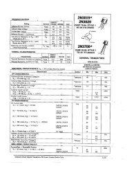
New - EBG - Darmstadt
New - EBG - Darmstadt
New - EBG - Darmstadt

You also want an ePaper? Increase the reach of your titles
YUMPU automatically turns print PDFs into web optimized ePapers that Google loves.
AQ-H<br />
CAUTIONS FOR USE<br />
1. For cautions regarding use, please<br />
refer to ’03-’04 Solid State Relays<br />
catalog.<br />
2. The internal IC could be damaged if<br />
a short forms between the I/O<br />
terminals while the solid state relay is<br />
powered.<br />
3. Output spike voltages<br />
1) The figure below shows an ordinary<br />
circuit. Please add a snubber circuit or<br />
varistor, as noise/surge on the load side<br />
could damage the unit or cause<br />
malfunctions.<br />
8. The following shows the packaging format<br />
1) Tape and reel<br />
4<br />
1 8<br />
2<br />
3<br />
4<br />
Type Tape dimensions Dimensions of paper tape reel<br />
8-pin SMD type<br />
6<br />
5<br />
Note) Connection of an external resister, etc.,<br />
to terminal No. 5 (gate) is not necessary.<br />
2) Even if spike voltages generated at the<br />
load are limited with a clamp diode if the<br />
circuit wires are long, spike voltages will<br />
occur by inductance. Keep wires as short<br />
as possible to minimize inductance.<br />
4. Ripple in the input power supply<br />
1) For LED operate current at Emin,<br />
maintain min. 10 mA<br />
2) Keep the LED operate current at 50 mA<br />
or less at Emax.<br />
Emin. Emax.<br />
4.5±0.3<br />
.177±.012<br />
Load<br />
0.3±0.05<br />
.012±.002<br />
VL(AC)<br />
5. When soldering terminals, keep<br />
soldering time to within 10s at 260°C<br />
500°F<br />
Device mounted<br />
on tape<br />
Tractor feed holes<br />
+0.1<br />
1.5 –0 dia.<br />
+.004<br />
.059 –0 dia.<br />
6. Cleaning<br />
The solid state relay forms an optical path<br />
by coupling a light-emitting diode (LED)<br />
and photodiode via transparent silicon<br />
resin.<br />
For this reason, avoid ultrasonic cleansing<br />
if at all possible.<br />
We recommend cleaning with an organic<br />
solvent. If you cannot avoid using<br />
ultrasonic cleansing, please ensure that<br />
the following conditions are met, and<br />
check beforehand for defects.<br />
• Frequency: 27 to 29 kHz<br />
• Ultrasonic output: No greater than 0.25<br />
W/cm 2<br />
• Cleaning time: No longer than 30<br />
seconds<br />
• Cleanser used: Asahiklin AK-225<br />
• Other: Submerge in solvent in order to<br />
prevent the PCB and elements from being<br />
contacted directly by the ultrasonic<br />
vibrations.<br />
Note: Applies to unit area ultrasonic output for<br />
ultrasonic baths.<br />
7. Soldering<br />
1) When soldering PC board terminals,<br />
keep soldering time to within 10 s at<br />
260°C 500°F.<br />
2) When soldering surface-mount<br />
terminals, the following conditions are<br />
recommended.<br />
(1) IR (Infrared reflow) soldering method<br />
Direction of picking<br />
4±0.1<br />
.157±.004<br />
12±0.1<br />
.472±.004<br />
10.1±0.1<br />
.400±.004<br />
2±0.1<br />
.079±.004<br />
1.75±0.1<br />
.069±.004<br />
7.5±0.1<br />
.295±.004<br />
16±0.3<br />
.630±.012<br />
10.2±0.1<br />
.402±.004<br />
1.55±0.1 dia.<br />
.061±.004 dia.<br />
(1) When picked from 1/2/3/4-pin side: Part No. AQH❍❍❍❍AX (Shown above)<br />
(2) When picked from 5/6/8-pin side: Part No. AQH❍❍❍❍AZ<br />
T3<br />
T2<br />
T1<br />
t1 t2<br />
T1 = 155 to 165°C 311 to 329°F<br />
T2 = 180°C 200°C 356 to 392°F<br />
T3 = 245°C 473°F or less<br />
t1 = 120 s or less<br />
t2 = 30 s or less<br />
2±0.5<br />
.079±.020<br />
(2) Vapor phase soldering method<br />
T2<br />
T1<br />
(3) Double wave soldering method<br />
T2<br />
T1<br />
t1 t2<br />
T1 = 180 to 200°C 366 to 392°F<br />
T2 = 215°C 419°F or less<br />
t1 = 40 s<br />
t2 = 90 s or less (40 s: SOP type)<br />
(4) Soldering iron method<br />
Tip temperature: 280 to 300°C 536 to<br />
572°F<br />
Wattage: 30 to 60 W<br />
Soldering time: within 5 seconds<br />
(5) Others<br />
Check mounting conditions before using<br />
other soldering methods (hot-air, hot<br />
plate, pulse heater, etc.)<br />
• The temperature profile indicates the<br />
temperature of the soldered terminal on<br />
the surface of the PC board. The ambient<br />
temperature may increase excessively.<br />
Check the temperature under mounting<br />
conditions.<br />
• The conditions for the infrared reflow<br />
soldering apply when preheating using<br />
the VPS method.<br />
21±0.8<br />
.827±.031<br />
80±1 dia.<br />
3.150±.039 dia.<br />
13±0.5 dia.<br />
.512±.020 dia.<br />
t1 t2 t3<br />
T1 = 155 to 165°C 311 to 329°F<br />
T2 = 260°C 500°F or less<br />
t1 = 60 s or less<br />
t2+t3 = 5 s or less<br />
17.5±2.0<br />
.689±.079<br />
2±0.5<br />
.079±.020<br />
mm inch<br />
300±2 dia.<br />
11.811±.079 dia.<br />
80±1 dia.<br />
3.150±.039 dia.