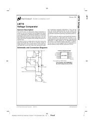
datasheet: pdf - Farnell
datasheet: pdf - Farnell
datasheet: pdf - Farnell

You also want an ePaper? Increase the reach of your titles
YUMPU automatically turns print PDFs into web optimized ePapers that Google loves.
■ OUTPUT SWITCH CURRENT IN EXCESS<br />
OF 1.5A<br />
■ 2% REFERENCE ACCURACY<br />
■ LOW QUIESCENT CURRENT: 2.5mA (TYP.)<br />
■ OPERATINGFROM3VTO40V<br />
■ FREQUENCY OPERATION TO 100KHz<br />
■ ACTIVE CURRENT LIMITING<br />
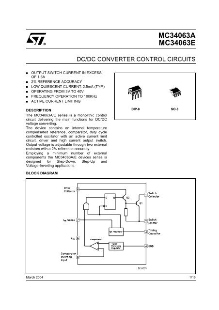
DESCRIPTION<br />
The MC34063A/E series is a monolithic control<br />
circuit delivering the main functions for DC/DC<br />
voltage converting.<br />
The device contains an internal temperature<br />
compensated reference, comparator, duty cycle<br />
controlled oscillator with an active current limit<br />
circuit, driver and high current output switch.<br />
Output voltage is adjustable through two external<br />
resistors with a 2% reference accuracy.<br />
Employing a minimum number of external<br />
components the MC34063A/E devices series is<br />
designed for Step-Down, Step-Up and<br />
Voltage-Inverting applications.<br />
BLOCK DIAGRAM<br />
March 2004<br />
MC34063A<br />
MC34063E<br />
DC/DC CONVERTER CONTROL CIRCUITS<br />
DIP-8 SO-8<br />
1/16
MC34063A/E<br />
ABSOLUTE MAXIMUM RATINGS<br />
Symbol Parameter Value Unit<br />
VCC Power Supply Voltage 50 V<br />
VIR Comparator Input Voltage Range -0.3 to 40 V<br />
VSWC Switch Collector Voltage 40 V<br />
VSWE Switch Emitter Voltage (VSWC =40V) 40 V<br />
VCE Switch Collector to Emitter Voltage 40 V<br />
VDC Driver Collector Voltage 40 V<br />
IDC Driver Collector Current 100 mA<br />
ISW Switch Current 1.5 A<br />
PTOT Power Dissipation at TA = 25°C for DIP-8<br />
for SO-8<br />
1.25<br />
0.625<br />
W<br />
TJ Operating Junction Temperature 150 °C<br />
TSTG Storage Temperature Range -40 to 150 °C<br />
Operating Ambient Temperature Range for AC and EC SERIES 0 to 70<br />
TOP for AB SERIES -40 to 85<br />
°C<br />
for EB SERIES -40 to 125<br />
Absolute Maximum Ratings are those values beyond which damage to the device may occur. Functional operation under these condition is<br />
not implied.<br />
THERMAL DATA<br />
Symbol Parameter DIP-8 SO-8 Unit<br />
Rthj-amb Thermal Resistance Junction-ambient (*) 100 160 °C/W<br />
Rthj-case Thermal Resistance Junction-case 42 20 °C/W<br />
(*) This value depends from thermal design of PCB on which the device is mounted.<br />
CONNECTION DIAGRAM (top view)<br />
PIN DESCRIPTION<br />
2/16<br />
Pin N° Symbol Name and Function<br />
1 SWC Switch Collector<br />
2 SWE Switch Emitter<br />
3 TC Timing Capacitor<br />
4 GND Ground<br />
5 CII Comparator Inverting Input<br />
6 VCC Voltage Supply<br />
7 IPK IPK Sense<br />
8 DRC Voltage Driver Collector
ORDERING CODES<br />
(*) The "A" version is not recommended for new designs.<br />
MC34063A/E<br />
TYPE DIP-8 SO-8 SO-8 (TAPE & REEL)<br />
MC34063AB MC34063ABN MC34063ABD MC34063ABD-TR<br />
MC34063AC MC34063ACN MC34063ACD MC34063ACD-TR<br />
MC34063EB MC34063EBN MC34063EBD MC34063EBD-TR<br />
MC34063EC MC34063ECN MC34063ECD MC34063ECD-TR<br />
ELECTRICAL CHARACTERISTICS (Refer to the test circuits, V CC =5V,T A =T LOW to T HIGH, unless<br />
otherwise specified, see note 2)<br />
OSCILLATOR<br />
Symbol Parameter Test Conditions Min. Typ. Max. Unit<br />
fOSC Frequency VPIN5 =0V CT =1nF TA = 25°C 24 33 42 KHz<br />
ICHG Charge Current VCC = 5 to 40V TA = 25°C 24 33 42 µA<br />
IDISCHG Discharge Current VCC = 5 to 40V TA = 25°C 140 200 260 µA<br />
IDISCHG /<br />
ICHG Discharge to Charge Current<br />
Ratio<br />
PIN 7 = VCC TA = 25°C 5.2 6.2 7.5 µA<br />
VIPK(sense) Current Limit Sense Voltage ICHG =IDISCHG TA = 25°C 250 300 350 mV<br />
OUTPUT SWITCH<br />
Symbol Parameter Test Conditions Min. Typ. Max. Unit<br />
VCE(sat) Saturation Voltage, Darlington<br />
Connection<br />
ISW = 1 A PIN 7, 8 connected 1 1.3 V<br />
VCE(sat) Saturation Voltage ISW =1A RPIN8 =82Ω to VCC 0.45 0.7 V<br />
Forced β ~20<br />
hFE DC Current Gain ISW =1A VCE =5V TA = 25°C 50 120<br />
IC(off) Collector Off-State Current VCE =40V 0.01 100 µA<br />
COMPARATOR<br />
Symbol Parameter Test Conditions Min. Typ. Max. Unit<br />
VTH Threshold Voltage TA = 25°C 1.225 1.25 1.275 V<br />
TA =TLOW to THIGH 1.21 1.29<br />
Regline Threshold Voltage Line<br />
Regulation<br />
VCC =3to40V 1 5 mV<br />
IIB Input Bias Current VIN = 0 V -5 -400 nA<br />
3/16
MC34063A/E<br />
TOTAL DEVICE<br />
Symbol Parameter Test Conditions Min. Typ. Max. Unit<br />
ICC Supply Current VCC =5to40V for MC34063A 2.5 4 mA<br />
CT =1nF<br />
PIN 7 = VCC VPIN5 >VTH PIN 2 = GND<br />
Remaining pins open<br />
for MC34063E<br />
1.5 4<br />
VSTART-UP Start-Up Voltage (Note 4) TA =25°C<br />
for MC34063A 2.1 V<br />
CT =1µF,PIN5=0 for MC34063E 1.5<br />
NOTES:<br />
1) Maximum package power dissipation limit must be observed.<br />
2) T LOW =0°C,T HIGH = 70°C (AC and EC series); T LOW =-40°C,T HIGH = 85°C (AB series); T LOW = -40°C, T HIGH = 125°C (EB series).<br />
3) If Darlington configuration is not used, care must be taken to avoid deep saturation of output switch. The resulting switch-off time may be<br />
adversely affected. In a Darlington configuration the following output driver condition is suggested:<br />
Forced β of output current switch = I COUTPUT /(I CDRIVER -1mA*)≥ 10<br />
* Current less due to a built in 1KΩ anti leakage resistor.<br />
4) Start-up Voltage is the minimum Power Supply Voltage at which the internal oscillator begins to work.<br />
TYPICAL PERFORMANCE CHARACTERISTICS<br />
Figure 1 : Emitter Follower Configuration Output<br />
Saturation Voltage vs Emitter Current<br />
Figure 2 : Output Switch ON-OFF Time vs<br />
Oscillator Timing Capacitor<br />
4/16<br />
Figure 3 : Common Emitter Configuration Output<br />
Switch Saturation Voltage vs Collector Current<br />
Figure 4 : Darlington Configuration Collector<br />
Emitter Saturation Voltage (V CEsat) vs Temperat.
Figure 5 : Power Collector Emitter Saturation<br />
Voltage (V CEsat) vs Temperature<br />
Figure 6 : Current Limit Sense Voltage (V IPK )vs<br />
Temperature<br />
Figure 7 : Reference Voltage vs Temperature<br />
Figure 8 : Bias Current vs Temperature<br />
MC34063A/E<br />
Figure 9 : Supply Current vs Temperature<br />
Figure 10 : Supply Current vs Input Voltage<br />
5/16
MC34063A/E<br />
TYPICAL APPLICATION CIRCUIT<br />
Step-UP Converter<br />
Printed Demoboard<br />
Test Condition (V OUT = 28V)<br />
6/16<br />
PIN 1 = V OUT<br />
PIN 2 = GND<br />
PIN 3 = GND<br />
PIN 4 = V IN<br />
Test Conditions Value (Typ.) Unit<br />
Line Regulation VIN =8to16V, IO = 175 mA 30 mV<br />
Load Regulation VIN =12V, IO =75to175mA 10 mV<br />
Output Ripple VIN =12V, IO = 175 mA 300 mV<br />
Efficiency VIN =12V, IO = 175 mA 89 %
Step-Down Converter<br />
Printed Demoboard<br />
Test Condition (V OUT =5V)<br />
PIN 1 = V OUT<br />
PIN 2 = GND<br />
PIN 3 = GND<br />
PIN 4 = V IN<br />
MC34063A/E<br />
Test Conditions Value (Typ.) Unit<br />
Line Regulation VIN =15to25V, IO = 500 mA 5 mV<br />
Load Regulation VIN =25V, IO =50to500mA 30 mV<br />
Output Ripple VIN =25V, IO = 500 mA 100 mV<br />
Efficiency VIN =25V, IO = 500 mA 80 %<br />
ISC VIN =25V, RLOAD =0.1Ω 1.2 A<br />
7/16
MC34063A/E<br />
Voltage Inverting Converter<br />
Printed Demoboard<br />
Test Condition (V OUT = -12V)<br />
Test Conditions Value (Typ.) Unit<br />
Line Regulation VIN = 4.5 to 6 V, IO = 100 mA 15 mV<br />
Load Regulation VIN =5V, IO =10to100mA 20 mV<br />
Output Ripple VIN =5V, IO = 100 mA 230 mV<br />
Efficiency VIN =5V, IO = 100 mA 58 %<br />
ISC VIN =5V, RLOAD =0.1Ω 0.9 A<br />
8/16<br />
PIN 1 = V OUT<br />
PIN 2 = GND<br />
PIN 3 = GND<br />
PIN 4 = V IN
Calculation<br />
Parameter<br />
Step-Up<br />
(Discontinuous mode)<br />
MC34063A/E<br />
NOTES:<br />
V SAT = Saturation voltage of the output switch<br />
V F = Forward voltage drop of the output rectifier<br />
THE FOLLOWING POWER SUPPLY CHARACTERISTICS MUST BE CHOSEN:<br />
V IN = Nominal input voltage<br />
V OUT = Desired output voltage, |V OUT | = 1.25(1+R 2 /R 1 )<br />
I OUT = Desired output current<br />
f MIN = Minimum desired output switching frequency at the selected values of V IN and I O<br />
V RIPPLE = Desired peak to peak output ripple voltage. In practice, the calculated capacitor value will and to be increased due to its equivalent<br />
series resistance and board layout. The ripple voltage should be kept to a low value since it will directly affect the line and load regulation.<br />
Step-Up With External NPN Switch<br />
Step-Down<br />
(Continuous mode)<br />
Voltage Inverting<br />
(Discontinuous mode)<br />
ton/toff (ton +toff) max 1/fmin 1/fmin 1/fmin CT 4.5x10⁻⁵ton 4.5x10⁻⁵ton 4.5x10⁻⁵ VOUT + VF – VIN( min)<br />
-------------------------------------------------------<br />
VIN( min)<br />
– Vsat VOUT + VF -----------------------------------------------------------<br />
VIN( min)<br />
– Vsat – VOUT VOUT + VF ------------------------------<br />
VIN – Vsat ton IPK(switch) 2Iout(max)[(ton/toff)+1] 2Iout(max) 2Iout(max)[(ton/toff)+1] RSC 0.3/IPK(switch) 0.3/IPK(switch) 0.3/IPK(switch) CO Ioutton -------------------------------<br />
Vripple( p – p)<br />
IPK( switch)<br />
( ton + toff) -----------------------------------------------------<br />
8Vripple( p – p)<br />
Ioutton -------------------------------<br />
Vripple( p – p)<br />
L (min)<br />
VIN( min)<br />
– Vsat -------------------------------------- × t<br />
I on( min)<br />
PK( switch)<br />
VIN( min)<br />
– Vsat – Vout ------------------------------------------------------- × t<br />
I on( min)<br />
PK( switch)<br />
VIN( min)<br />
– Vsat -------------------------------------- ×<br />
t<br />
I on( min)<br />
PK( switch)<br />
9/16
MC34063A/E<br />
Step-Down With External NPN Switch<br />
Step-Down With External PNP Switch<br />
10/16
Voltage Inverting With External NPN Switch<br />
Voltage Inverting With External PNP Saturated Switch<br />
MC34063A/E<br />
11/16
MC34063A/E<br />
Dual Output Voltage<br />
Higher Output Power, Higher Input Voltage<br />
12/16
DIM.<br />
Plastic DIP-8 MECHANICAL DATA<br />
mm. inch<br />
MC34063A/E<br />
MIN. TYP MAX. MIN. TYP. MAX.<br />
A 3.3 0.130<br />
a1 0.7 0.028<br />
B 1.39 1.65 0.055 0.065<br />
B1 0.91 1.04 0.036 0.041<br />
b 0.5 0.020<br />
b1 0.38 0.5 0.015 0.020<br />
D 9.8 0.386<br />
E 8.8 0.346<br />
e 2.54 0.100<br />
e3 7.62 0.300<br />
e4 7.62 0.300<br />
F 7.1 0.280<br />
I 4.8 0.189<br />
L 3.3 0.130<br />
Z 0.44 1.6 0.017 0.063<br />
P001F<br />
13/16
MC34063A/E<br />
14/16<br />
DIM.<br />
SO-8 MECHANICAL DATA<br />
mm. inch<br />
MIN. TYP MAX. MIN. TYP. MAX.<br />
A 1.35 1.75 0.053 0.069<br />
A1 0.10 0.25 0.04 0.010<br />
A2 1.10 1.65 0.043 0.065<br />
B 0.33 0.51 0.013 0.020<br />
C 0.19 0.25 0.007 0.010<br />
D 4.80 5.00 0.189 0.197<br />
E 3.80 4.00 0.150 0.157<br />
e 1.27 0.050<br />
H 5.80 6.20 0.228 0.244<br />
h 0.25 0.50 0.010 0.020<br />
L 0.40 1.27 0.016 0.050<br />
k 8˚<br />
(max.)<br />
ddd 0.1 0.04<br />
0016023/C
DIM.<br />
Tape & Reel SO-8 MECHANICAL DATA<br />
mm. inch<br />
MC34063A/E<br />
MIN. TYP MAX. MIN. TYP. MAX.<br />
A 330 12.992<br />
C 12.8 13.2 0.504 0.519<br />
D 20.2 0.795<br />
N 60 2.362<br />
T 22.4 0.882<br />
Ao 8.1 8.5 0.319 0.335<br />
Bo 5.5 5.9 0.216 0.232<br />
Ko 2.1 2.3 0.082 0.090<br />
Po 3.9 4.1 0.153 0.161<br />
P 7.9 8.1 0.311 0.319<br />
15/16
MC34063A/E<br />
Information furnished is believed to be accurate and reliable. However, STMicroelectronics assumes no responsibility for the<br />
consequences of use of such information nor for any infringement of patents or other rights of third parties which may result from<br />
its use. No license is granted by implication or otherwise under any patent or patent rights of STMicroelectronics. Specifications<br />
mentioned in this publication are subject to change without notice. This publication supersedes and replaces all information<br />
previously supplied. STMicroelectronics products are not authorized for use as critical components in life support devices or<br />
systems without express written approval of STMicroelectronics.<br />
The ST logo is a registered trademark of STMicroelectronics<br />
All other names are the property of their respective owners<br />
© 2004 STMicroelectronics - All Rights Reserved<br />
STMicroelectronics GROUP OF COMPANIES<br />
Australia - Belgium - Brazil - Canada - China - Czech Republic - Finland - France - Germany - Hong Kong - India - Israel - Italy - Japan -<br />
Malaysia - Malta - Morocco - Singapore - Spain - Sweden - Switzerland - United Kingdom - United States.<br />
http://www.st.com<br />
16/16