

Chapter 1 Introduction to Chemical Vapor Deposition (CVD)
Chapter 1 Introduction to Chemical Vapor Deposition (CVD)
Chapter 1 Introduction to Chemical Vapor Deposition (CVD)

You also want an ePaper? Increase the reach of your titles
YUMPU automatically turns print PDFs into web optimized ePapers that Google loves.
© 2001 ASM International. All Rights Reserved.<br />
<strong>Chemical</strong> <strong>Vapor</strong> <strong>Deposition</strong> (#06682G)<br />
<strong>Chapter</strong> 1<br />
<strong>Introduction</strong> <strong>to</strong> <strong>Chemical</strong> <strong>Vapor</strong><br />
<strong>Deposition</strong> (<strong>CVD</strong>)<br />
J. R. Creigh<strong>to</strong>n and P. Ho<br />
Sandia National Labora<strong>to</strong>ries<br />
P.O. Box 5800, MS0601<br />
Albuquerque, NM 87185-0601<br />
<strong>Introduction</strong><br />
<strong>Chemical</strong> vapor deposition (<strong>CVD</strong>) is a<br />
widely used materials-processing technology.<br />
The majority of its applications involve applying<br />
solid thin-film coatings <strong>to</strong> surfaces, but it is also<br />
used <strong>to</strong> produce high-purity bulk materials and<br />
powders, as well as fabricating composite<br />
materials via infiltration techniques. It has been<br />
used <strong>to</strong> deposit a very wide range of materials.<br />
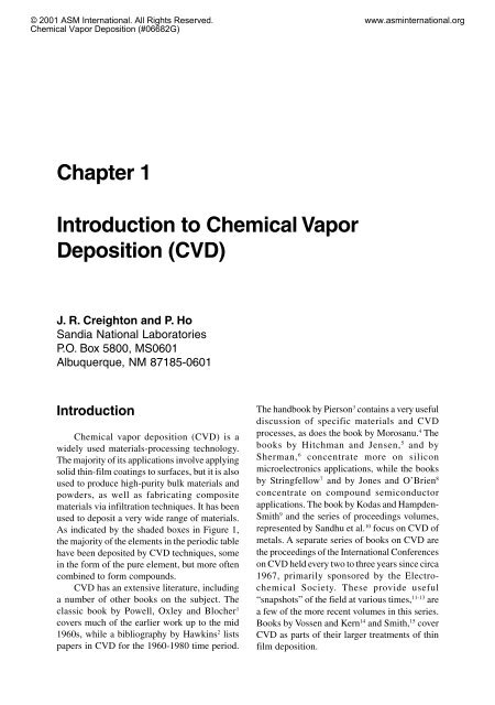
As indicated by the shaded boxes in Figure 1,<br />
the majority of the elements in the periodic table<br />
have been deposited by <strong>CVD</strong> techniques, some<br />
in the form of the pure element, but more often<br />
combined <strong>to</strong> form compounds.<br />
<strong>CVD</strong> has an extensive literature, including<br />
a number of other books on the subject. The<br />
classic book by Powell, Oxley and Blocher 1<br />
covers much of the earlier work up <strong>to</strong> the mid<br />
1960s, while a bibliography by Hawkins 2 lists<br />
papers in <strong>CVD</strong> for the 1960-1980 time period.<br />
www.asminternational.org<br />
The handbook by Pierson 3 contains a very useful<br />
discussion of specific materials and <strong>CVD</strong><br />
processes, as does the book by Morosanu. 4 The<br />
books by Hitchman and Jensen, 5 and by<br />
Sherman, 6 concentrate more on silicon<br />
microelectronics applications, while the books<br />
by Stringfellow 7 and by Jones and O’Brien 8<br />
concentrate on compound semiconduc<strong>to</strong>r<br />
applications. The book by Kodas and Hampden-<br />
Smith 9 and the series of proceedings volumes,<br />
represented by Sandhu et al. 10 focus on <strong>CVD</strong> of<br />
metals. A separate series of books on <strong>CVD</strong> are<br />
the proceedings of the International Conferences<br />
on <strong>CVD</strong> held every two <strong>to</strong> three years since circa<br />
1967, primarily sponsored by the Electrochemical<br />
Society. These provide useful<br />
“snapshots” of the field at various times, 11-13 are<br />
a few of the more recent volumes in this series.<br />
Books by Vossen and Kern 14 and Smith, 15 cover<br />
<strong>CVD</strong> as parts of their larger treatments of thin<br />
film deposition.
© 2001 ASM International. All Rights Reserved.<br />
<strong>Chemical</strong> <strong>Vapor</strong> <strong>Deposition</strong> (#06682G)<br />
2<br />
PERIODIC TABLE<br />
IA IIA IIIA IVA VA VIA VIIA VIII IB IIB IIIB IV VA VIB VIIB O<br />
Creigh<strong>to</strong>n and Ho<br />
2<br />
He<br />
4.003<br />
1<br />
H<br />
1.008<br />
10<br />
Ne<br />
20.179<br />
9<br />
F<br />
19.00<br />
8<br />
O<br />
16.00<br />
7<br />
N<br />
14.01<br />
6<br />
C<br />
12.01<br />
5<br />
B<br />
10.81<br />
4<br />
Be<br />
9.012<br />
3<br />
Li<br />
6.941<br />
18<br />
Ar<br />
39.948<br />
17<br />
CI<br />
35.45<br />
16<br />
S<br />
32.07<br />
15<br />
P<br />
30.97<br />
14<br />
Si<br />
28.09<br />
13<br />
Al<br />
26.98<br />
12<br />
Mg<br />
24.305<br />
11<br />
Na<br />
22.990<br />
36<br />
Kr<br />
83.80<br />
35<br />
Br<br />
79.90<br />
34<br />
Se<br />
78.96<br />
33<br />
As<br />
74.92<br />
32<br />
Ge<br />
72.61<br />
31<br />
Ga<br />
69.72<br />
30<br />
Zn<br />
65.39<br />
29<br />
Cu<br />
63.546<br />
28<br />
Ni<br />
58.70<br />
27<br />
Co<br />
58.933<br />
26<br />
Fe<br />
55.847<br />
25<br />
Mn<br />
54.938<br />
24<br />
Cr<br />
51.996<br />
23<br />
V<br />
50.942<br />
22<br />
Ti<br />
47.90<br />
21<br />
Sc<br />
44.956<br />
20<br />
Ca<br />
40.08<br />
19<br />
K<br />
39.098<br />
54<br />
Xe<br />
131.30<br />
86<br />
Rn<br />
(222)<br />
53<br />
I<br />
126.9<br />
52<br />
Te<br />
127.6<br />
51<br />
Sb<br />
121.8<br />
50<br />
Sn<br />
118.7<br />
49<br />
In<br />
114.8<br />
48<br />
Cd<br />
112.4<br />
47<br />
Ag<br />
107.868<br />
46<br />
Pd<br />
106.4<br />
45<br />
Rh<br />
102.905<br />
44<br />
Ru<br />
101.07<br />
43<br />
Tc<br />
(99)<br />
42<br />
Mo<br />
95.94<br />
41<br />
Nb<br />
92.906<br />
40<br />
Zr<br />
91.22<br />
39<br />
Y<br />
88.906<br />
38<br />
Sr<br />
87.62<br />
37<br />
Rb<br />
85.468<br />
85<br />
At<br />
(210)<br />
84<br />
Po<br />
(210)<br />
83<br />
Bi<br />
209.0<br />
82<br />
Pb<br />
207.2<br />
81<br />
TI<br />
204.37<br />
80<br />
Hg<br />
200.59<br />
79<br />
Au<br />
196.966<br />
78<br />
Pt<br />
195.09<br />
77<br />
Ir<br />
192.22<br />
76<br />
Os<br />
190.2<br />
75<br />
Re<br />
186.2<br />
74<br />
W<br />
183.85<br />
73<br />
Ta<br />
180.948<br />
72<br />
Hf<br />
178.49<br />
57<br />
La<br />
138.9<br />
89<br />
Ac<br />
227.0<br />
56<br />
Ba<br />
137.33<br />
88<br />
Ra<br />
(226)<br />
55<br />
Cs<br />
132.905<br />
87<br />
Fr<br />
(223)<br />
www.asminternational.org<br />
71<br />
Lu<br />
174.96<br />
103<br />
Lr<br />
(257)<br />
70<br />
Yb<br />
173.0<br />
69<br />
Tm<br />
168.9<br />
68<br />
Er<br />
167.3<br />
67<br />
Ho<br />
164.9<br />
66<br />
Dy<br />
162.5<br />
65<br />
Tb<br />
158.9<br />
64<br />
Gd<br />
157.2<br />
63<br />
Eu<br />
152.0<br />
62<br />
Sm<br />
150.4<br />
61<br />
Pm<br />
(145)<br />
60<br />
Nd<br />
144.2<br />
59<br />
Pr<br />
140.1<br />
58<br />
Ce<br />
140.115<br />
57<br />
La<br />
138.9<br />
LANTHANIDES<br />
102<br />
No<br />
(259)<br />
101<br />
Md<br />
(256)<br />
100<br />
Fm<br />
(257)<br />
99<br />
Es<br />
(252)<br />
98<br />
Cf<br />
(251)<br />
97<br />
Bk<br />
(247)<br />
96<br />
Cm<br />
(247)<br />
95<br />
Am<br />
(243)<br />
94<br />
Pu<br />
(244)<br />
93<br />
Np<br />
237.0<br />
92<br />
U<br />
238.0<br />
91<br />
Pa<br />
231.0<br />
90<br />
Th<br />
232.0<br />
89<br />
Ac<br />
227.0<br />
ACTINIDES<br />
Fig. 1: Periodic table, where shaded boxes indicate elements that have been deposited using <strong>CVD</strong>.
© 2001 ASM International. All Rights Reserved.<br />
<strong>Chemical</strong> <strong>Vapor</strong> <strong>Deposition</strong> (#06682G)<br />
In its simplest incarnation, <strong>CVD</strong> involves<br />
flowing a precursor gas or gases in<strong>to</strong> a chamber<br />
containing one or more heated objects <strong>to</strong> be<br />
coated. <strong>Chemical</strong> reactions occur on and near<br />
the hot surfaces, resulting in the deposition of a<br />
thin film on the surface. This is accompanied by<br />
the production of chemical by-products that are<br />
exhausted out of the chamber along with<br />
unreacted precursor gases. As would be expected<br />
with the large variety of materials deposited and<br />
the wide range of applications, there are many<br />
variants of <strong>CVD</strong>. It is done in hot-wall reac<strong>to</strong>rs<br />
and cold-wall reac<strong>to</strong>rs, at sub-<strong>to</strong>rr <strong>to</strong>tal pressures<br />
<strong>to</strong> above-atmospheric pressures, with and<br />
without carrier gases, and at temperatures<br />
typically ranging from 200-1600°C. There are<br />
also a variety of enhanced <strong>CVD</strong> processes,<br />
which involve the use of plasmas, ions, pho<strong>to</strong>ns,<br />
lasers, hot filaments, or combustion reactions <strong>to</strong><br />
increase deposition rates and/or lower deposition<br />
temperatures. There are also many derivatives<br />
of the <strong>CVD</strong> terminology, such as metal-organic<br />
chemical vapor deposition (MO<strong>CVD</strong>) 16,17 or, less<br />
commonly, organo-metallic chemical vapor<br />
deposition (OM<strong>CVD</strong>), which are sometimes<br />
used <strong>to</strong> note the class of molecules used in the<br />
deposition process. Some practitioners chose <strong>to</strong><br />
differentiate epitaxial film deposition from<br />
polycrystalline or amorphous film deposition,<br />
so they introduced a variety of terms that include<br />
“epitaxy” in the acronym. Two of the more<br />
common variants are organometallic vapor phase<br />
epitaxy (OMVPE) 7 and metalorganic vapor<br />
phase epitaxy (MOVPE) 18 which are often used<br />
in the compound semiconduc<strong>to</strong>r epitaxy<br />
literature.<br />
<strong>CVD</strong> has a number of advantages as a<br />
method for depositing thin films. One of the<br />
primary advantages is that <strong>CVD</strong> films are<br />
generally quite conformal, i.e., that the film<br />
thickness on the sidewalls of features is<br />
comparable <strong>to</strong> the thickness on the <strong>to</strong>p. This<br />
means that films can be applied <strong>to</strong> elaborately<br />
shaped pieces, including the insides and<br />
undersides of features, and that high-aspect ratio<br />
holes and other features can be completely filled.<br />
In contrast, physical vapor deposition (PVD)<br />
techniques, such as sputtering or evaporation,<br />
generally require a line-of-sight between the<br />
<strong>Introduction</strong> <strong>to</strong> <strong>Chemical</strong> <strong>Vapor</strong> <strong>Deposition</strong> 3<br />
surface <strong>to</strong> be coated and the source. Another<br />
advantage of <strong>CVD</strong> is that, in addition <strong>to</strong> the wide<br />
variety of materials that can be deposited, they<br />
can be deposited with very high purity. This<br />
results from the relative ease with which<br />
impurities are removed from gaseous precursors<br />
using distillation techniques. Other advantages<br />
include relatively high deposition rates, and the<br />
fact that <strong>CVD</strong> often doesn’t require as high a<br />
vacuum as PVD processes.<br />
<strong>CVD</strong> also has a number of disadvantages.<br />
One of the primary disadvantages lies in the<br />
properties of the precursors. Ideally, the<br />
precursors need <strong>to</strong> be volatile at near-room<br />
temperatures. This is non-trivial for a number<br />
of elements in the periodic table, although the<br />
use of metal-organic precursors has eased this<br />
situation. <strong>CVD</strong> precursors can also be highly<br />
<strong>to</strong>xic (Ni(CO) 4 ), explosive (B 2 H 6 ), or corrosive<br />
(SiCl 4 ). The byproducts of <strong>CVD</strong> reactions can<br />
also be hazardous (CO, H 2 , or HF). Some of<br />
these precursors, especially the metal-organic<br />
precursors, can also be quite costly. The other<br />
major disadvantage is the fact that the films are<br />
usually deposited at elevated temperatures. This<br />
puts some restrictions on the kind of substrates<br />
that can be coated. More importantly, it leads <strong>to</strong><br />
stresses in films deposited on materials with<br />
different thermal expansion coefficients, which<br />
can cause mechanical instabilities in the<br />
deposited films.<br />
<strong>CVD</strong> processes can be categorized<br />
according <strong>to</strong> the type of:<br />
1. Application,<br />
2. Process and reac<strong>to</strong>r used, or<br />
3. Precursor and chemical reaction used.<br />
The next three sections of this chapter are<br />
arranged around such subdivisions. These<br />
sections are followed by a discussion of the<br />
fundamental processes underlying <strong>CVD</strong>, such<br />
as mass transport, thermodynamics, and<br />
chemical kinetics. Finally, we present a brief<br />
analysis of the his<strong>to</strong>rical and current status of<br />
<strong>CVD</strong> R & D.<br />
<strong>CVD</strong> Applications<br />
www.asminternational.org<br />
One of the earliest examples of a large-scale<br />
<strong>CVD</strong> application was a carbonyl process for
© 2001 ASM International. All Rights Reserved.<br />
<strong>Chemical</strong> <strong>Vapor</strong> <strong>Deposition</strong> (#06682G)<br />
4<br />
Creigh<strong>to</strong>n and Ho<br />
refining of nickel, as developed by Mond,<br />
Langer, and Quincke in 1890. 19 Many of the<br />
early applications involved refining or<br />
purification of metals and a limited number of<br />
non-metals by carbonyl or halide processes.<br />
Other early applications involved deposition of<br />
coatings for wear and corrosion resistance, and<br />
the fabrication of structural shapes and<br />
components. Most of the earliest work, up <strong>to</strong><br />
the mid 1960s, is reviewed in the book by<br />
Powell, Oxley, and Blocher. 1 Many high volume<br />
applications, such as refining and the production<br />
of powders and pigments, are obviously still<br />
important economically, but most of the recent<br />
<strong>CVD</strong> R & D effort is aimed at thin-film<br />
deposition.<br />
There is a great deal of ongoing R & D<br />
regarding <strong>CVD</strong> of thin films used primarily for<br />
their mechanical or chemical properties. Many<br />
of these are discussed in detail in other chapters<br />
of this book, so we only briefly mention them<br />
here. <strong>Chapter</strong> 11 discusses the use of <strong>CVD</strong> films<br />
for tribological applications, chapter 13<br />
discusses <strong>CVD</strong> films used for corrosion<br />
protection, and chapter 14 discusses protective<br />
<strong>CVD</strong> coatings for <strong>to</strong>ol steels. <strong>Chapter</strong> 10<br />
discusses the <strong>CVD</strong> of diamond, and diamondlike<br />
carbon (DLC), which has generated a<br />
tremendous interest level in the past decade (see<br />
also last section, this chapter), and has significant<br />
commercial applications. Diamond films are<br />
mainly used for their hardness, but applications<br />
utilizing its high thermal conductivity, chemical<br />
inertness, or electronic properties are also<br />
important.<br />
A great deal of <strong>CVD</strong> R & D in recent<br />
decades, however, is focussed on the<br />
semiconduc<strong>to</strong>r revolution. We devote somewhat<br />
more space here <strong>to</strong> these applications, as they<br />
are not covered elsewhere in this book. <strong>CVD</strong><br />
has been a critical enabling technology in<br />
silicon-based microelectronics; it is even used<br />
at the earliest stage during the refining and<br />
purification of elemental silicon. Depending on<br />
the device, <strong>CVD</strong> processes are used for<br />
depositing thin films of the active semiconduc<strong>to</strong>r<br />
material (e.g. doped Si), conductive<br />
interconnects (e.g. tungsten), and/or insulating<br />
dielectrics (e.g. SiO 2 ), (see Figure 2).<br />
www.asminternational.org<br />
The communications revolution also relies<br />
on a diverse set of <strong>CVD</strong> technologies. Some<br />
components are similar <strong>to</strong> those used in silicon<br />
microelectronics, but many are unique, involving<br />
complex epitaxial heterostructures of SiGe or<br />
compound semiconduc<strong>to</strong>r (e.g., AlGaAs) alloys<br />
that are required <strong>to</strong> yield high frequency (1-100<br />
GHz) device operation. 20 The communication<br />
revolution also relies on op<strong>to</strong>electronic<br />
components, such as solid state diode lasers<br />
(another complex heterostructure device), and<br />
these devices are often grown by <strong>CVD</strong>. 7,21 Even<br />
the fiberoptic cables that transmit the optical<br />
component of the communications network are<br />
manufactured using a <strong>CVD</strong> technique <strong>to</strong> achieve<br />
the desired refractive index profile. 22<br />
Op<strong>to</strong>electronic material grown by <strong>CVD</strong> has<br />
many applications outside of the<br />
communications industry. One example is for<br />
solid state lighting using light emitting diodes<br />
(LEDs). Recently, Nichia <strong>Chemical</strong> was the first<br />
company <strong>to</strong> commercialize high brightness blue<br />
and green LEDs based on group-III nitride<br />
alloys, e.g. InGaN, which are grown on sapphire<br />
substrates using <strong>CVD</strong> technology. 23 This<br />
company also introduced the first long-life blue<br />
laser diode, based on the same material and<br />
technology. In addition <strong>to</strong> the myriad of lighting<br />
and signage applications using colored LEDs,<br />
there is a growing interest in generating solid<br />
state white light sources <strong>to</strong> replace incandescent<br />
and perhaps even fluorescent sources. 24 A solidstate<br />
white light source may be achieved by<br />
combining LEDs of different wavelengths, or<br />
by pumping a phosphor with an ultraviolet LED.<br />
Another exciting technology utilizing <strong>CVD</strong><br />
is the production of microelectromechanical<br />
structures, or MEMS. 25 Much of the MEMS<br />
technology is derived from the silicon<br />
microelectronics technology, so it is not<br />
surprising that <strong>CVD</strong> plays a crucial role. Most<br />
MEMS devices are fabricated from<br />
polycrystalline silicon (polysilicon) films<br />
deposited on silicon wafers, with intermediate<br />
sacrificial SiO 2 layers that are later removed by<br />
chemical etching. Figure 3 shows an example<br />
of such a device, in this case a set of interlocking<br />
gears that are ~50-200 microns in diameter. Both<br />
the polysilicon and oxide are deposited using
© 2001 ASM International. All Rights Reserved.<br />
<strong>Chemical</strong> <strong>Vapor</strong> <strong>Deposition</strong> (#06682G)<br />
<strong>CVD</strong> or PE<strong>CVD</strong>. The <strong>CVD</strong> steps define the<br />
structure of the device perpendicular <strong>to</strong> the<br />
silicon substrate, while numerous lithographic<br />
and etching steps define the structure in the other<br />
two dimensions. <strong>CVD</strong> is sometimes used <strong>to</strong><br />
apply coatings <strong>to</strong> reduce friction after the 3-D<br />
structure is created. Work is also being done <strong>to</strong><br />
integrate MEMS devices with silicon<br />
microelectronic devices on the same chip.<br />
The field of nanotechnology has generated<br />
a lot of recent interest, and focused research<br />
programs have been initiated in almost all<br />
industrialized countries in the last five years. In<br />
2000 the U.S. launched the National Nanotechnology<br />
Initiative, with plans <strong>to</strong> nearly double<br />
the nanoscale R & D effort. 26 Nano-technology<br />
is an extremely diverse <strong>to</strong>pic, but some of the<br />
best examples of existing nanoscale R & D are in<br />
the area of epitaxial heterostructures for laser<br />
diodes and LEDs grown by <strong>CVD</strong>. 7,23,27 Many of<br />
www.asminternational.org<br />
<strong>Introduction</strong> <strong>to</strong> <strong>Chemical</strong> <strong>Vapor</strong> <strong>Deposition</strong> 5<br />
Fig. 2: Cross section of a silicon microelectronic memory circuit showing several materials<br />
deposited by <strong>CVD</strong>; polycrystalline silicon, tungsten (W), SiO 2 , and Si 3 N 4 . Pho<strong>to</strong> courtesy<br />
of Pat Shea, Sandia National Labora<strong>to</strong>ries.<br />
these devices contain two dimensional (2-D)<br />
quantum wells or superlattices composed of<br />
strained epitaxial layers that are 1-10 nm thick.<br />
An example of a strained layer superlattice is<br />
shown in Figure 4. In addition <strong>to</strong> quantum wells,<br />
laser structures such as the vertical cavity surface<br />
emitting laser (VCSEL) contain mirror stacks<br />
composed of a large number of alternating layers<br />
of semiconduc<strong>to</strong>r material that are typically<br />
50-100 nm thick. The thickness of each layer<br />
often must be controlled with a precision better<br />
than 1 nm. Despite this requirement these<br />
devices can be grown routinely with relatively<br />
high yield in finely tuned and calibrated OMVPE<br />
reac<strong>to</strong>rs. 28 A related <strong>CVD</strong> technique that<br />
au<strong>to</strong>matically yields subnanometer control is<br />
known as a<strong>to</strong>mic layer epitaxy (ALE). 29<br />
An extension of 2-D quantum well R & D<br />
involves the generation of quantum wires (1-D)<br />
and quantum dots (0-D). 27,30 Quantum dots are
© 2001 ASM International. All Rights Reserved.<br />
<strong>Chemical</strong> <strong>Vapor</strong> <strong>Deposition</strong> (#06682G)<br />
6<br />
Creigh<strong>to</strong>n and Ho<br />
www.asminternational.org<br />
Fig. 3: Example of a silicon surface micromachined gear train. Courtesy of the Intelligent<br />
Micromachine Initiative, Sandia National Labora<strong>to</strong>ries.<br />
Fig. 4: Strained layer superlattice of InAsSb on InSb with 10 nm layer thickness. Pho<strong>to</strong> courtesy<br />
of R. M. Biefeld, Sandia National Labora<strong>to</strong>ries.
© 2001 ASM International. All Rights Reserved.<br />
<strong>Chemical</strong> <strong>Vapor</strong> <strong>Deposition</strong> (#06682G)<br />
often considered <strong>to</strong> be artificial a<strong>to</strong>ms, where<br />
the effect of quantum confinement significantly<br />
perturbs the normal bulk electronic properties<br />
of the material. One method of growing quantum<br />
dots involves depositing one material on another<br />
with a large lattice mismatch. The example in<br />
Figure 5 is InAs on GaAs(100) by <strong>CVD</strong>. Due <strong>to</strong><br />
the interfacial properties of this highly strained<br />
layer, InAs spontaneously forms islands on the<br />
10-nm scale with a relatively narrow size<br />
distribution. The electronic and optical<br />
properties of the InAs quantum dots are<br />
dramatically different from bulk InAs, allowing<br />
for novel device fabrication.<br />
In addition <strong>to</strong> the numerous electronic and<br />
op<strong>to</strong>electronic applications mentioned above,<br />
novel applications of <strong>CVD</strong> are also being used<br />
<strong>to</strong> generate macroscopic components (10 cm as<br />
opposed <strong>to</strong> 1 nm). One interesting example is<br />
the production of Ir/Re thrust chambers for liquid<br />
rocket mo<strong>to</strong>rs (see Figure 6). 31 For this structure<br />
<strong>Introduction</strong> <strong>to</strong> <strong>Chemical</strong> <strong>Vapor</strong> <strong>Deposition</strong> 7<br />
Fig. 5: Indium arsenide quantum dots deposited on gallium arsenide by OMVPE. Pho<strong>to</strong> courtesy<br />
of Jeff Cederberg and R. M. Biefeld, Sandia National Labora<strong>to</strong>ries.<br />
a thick Rhenium <strong>CVD</strong> coating is applied <strong>to</strong> a<br />
sacrificial molybdenum mandrel, which is later<br />
removed by etching. Another example is the<br />
production of large-scale infrared optical materials<br />
(ZnSe and/or ZnS up <strong>to</strong> several feet across). 32<br />
<strong>CVD</strong> Reac<strong>to</strong>r Types<br />
www.asminternational.org<br />
As mentioned in the introduction, <strong>CVD</strong><br />
encompasses a wide range of reac<strong>to</strong>r and process<br />
types. The choice of process/reac<strong>to</strong>r is<br />
determined by the application via the<br />
requirements for substrate material, coating<br />
material and morphology, film thickness and<br />
uniformity, availability of precursors, and cost.<br />
Here, we discuss the general types of reac<strong>to</strong>rs<br />
used for <strong>CVD</strong>, and refer the reader <strong>to</strong> the other<br />
chapters in this and other books for detailed<br />
information on specific systems.<br />
Hot wall reac<strong>to</strong>rs represent one of the major<br />
categories of <strong>CVD</strong> reac<strong>to</strong>rs. In such systems,
© 2001 ASM International. All Rights Reserved.<br />
<strong>Chemical</strong> <strong>Vapor</strong> <strong>Deposition</strong> (#06682G)<br />
8<br />
Creigh<strong>to</strong>n and Ho<br />
Fig. 6: Rhenium rocket thrust chamber fabricated using <strong>CVD</strong>. Pho<strong>to</strong> courtesy of B. H. Tuffias,<br />
Ultramet. 31<br />
shown schematically in Figure 7, the chamber<br />
containing the parts is surrounded by a furnace<br />
that heats the system. The parts are loaded in<strong>to</strong><br />
the system, it is heated <strong>to</strong> the desired<br />
temperature, then the reactive gases are<br />
introduced. The reac<strong>to</strong>r may be equipped with<br />
shelves for coating many parts at once, or be<br />
sized for specific large parts. These systems are<br />
often run at very high temperatures, limited only<br />
by the materials used in constructing the furnace,<br />
and at reduced pressures, on the order of Torr <strong>to</strong><br />
tens of Torr. Figure 8 shows a schematic for a<br />
hot-wall reac<strong>to</strong>r that has been tailored <strong>to</strong> lowpressure<br />
<strong>CVD</strong> (LP<strong>CVD</strong>) batch processing in the<br />
microelectronics industry. In this case, a<br />
specialized support holds a large number (over<br />
a hundred) of closely-spaced silicon wafers for<br />
simultaneous processing. In general, hot wall<br />
reac<strong>to</strong>rs have the advantages of being able <strong>to</strong><br />
process large batches of substrates, and having<br />
www.asminternational.org<br />
relatively uniform substrate temperatures and<br />
thus coating thicknesses. The primary<br />
disadvantages are that the walls get heavily<br />
coated, requiring frequent cleaning and causing<br />
particle problems, and that it involves higher<br />
thermal loads and energy usage.<br />
Cold wall reac<strong>to</strong>rs are the other major<br />
category of <strong>CVD</strong> reac<strong>to</strong>rs. In such systems, the<br />
substrates are heated but the walls are cooled.<br />
Figure 9 shows an example of a cold wall<br />
rotating disk <strong>CVD</strong> reac<strong>to</strong>r. 28,33 This system has<br />
water-cooled quartz walls, with a rotating holder<br />
for (silicon or compound semiconduc<strong>to</strong>r) wafers<br />
that is resistively heated from below. Other<br />
commercial cold-wall reac<strong>to</strong>rs include lamp<br />
heated single-wafer reac<strong>to</strong>rs that are widely used<br />
in microelectronics fabrication, and inductively<br />
heated horizontal flow reac<strong>to</strong>rs. Cold-wall<br />
reac<strong>to</strong>rs are often run at relatively high pressures,<br />
several hundred <strong>to</strong>rr <strong>to</strong> atmospheric <strong>to</strong>tal
© 2001 ASM International. All Rights Reserved.<br />
<strong>Chemical</strong> <strong>Vapor</strong> <strong>Deposition</strong> (#06682G)<br />
<strong>Introduction</strong> <strong>to</strong> <strong>Chemical</strong> <strong>Vapor</strong> <strong>Deposition</strong> 9<br />
Fig. 7: Schematic drawing of hot-wall <strong>CVD</strong> reac<strong>to</strong>r used <strong>to</strong> coat multiple parts.<br />
Gas Inlet<br />
Gas Inlet<br />
Exhaust<br />
<strong>to</strong> Pump<br />
Heating<br />
Elements<br />
Parts<br />
Being<br />
Coated<br />
Shelves<br />
Heating<br />
Elements<br />
Wafers<br />
Exhaust <strong>to</strong> Pump<br />
www.asminternational.org<br />
Fig. 8: Schematic drawing of LP<strong>CVD</strong> furnace for batch processing of multiple silicon wafers.
© 2001 ASM International. All Rights Reserved.<br />
<strong>Chemical</strong> <strong>Vapor</strong> <strong>Deposition</strong> (#06682G)<br />
10<br />
Creigh<strong>to</strong>n and Ho<br />
Window for<br />
Pyrometry<br />
Rotating<br />
Water Holder<br />
Stationary<br />
Heater<br />
Screens for<br />
Straightening<br />
Gas Flow<br />
Water Cooled<br />
Quartz Walls<br />
Exhaust<br />
<strong>to</strong> Pump<br />
Gas Inlet<br />
Fig. 9: Schematic diagram of a cold-wall rotating disk <strong>CVD</strong> reac<strong>to</strong>r used for depositing thin films<br />
on semiconduc<strong>to</strong>r wafers.<br />
pressure, and usually have the reactive precursors<br />
diluted in a carrier gas. Most compound<br />
semiconduc<strong>to</strong>r <strong>CVD</strong> processes use reac<strong>to</strong>rs of<br />
this type. Cold wall reac<strong>to</strong>rs have the advantages<br />
of reduced deposition of material on the walls,<br />
which means less cleaning, lower thermal loads<br />
on the substrates because of faster heat-up and<br />
cool-down times, lower energy consumption, and<br />
the avoidance of vacuum equipment. The primary<br />
disadvantages are larger temperature nonuniformities<br />
on the substrate, which may lead <strong>to</strong><br />
film thickness non-uniformities, the smaller batch<br />
sizes, and possible thermal stresses on the<br />
substrates if the heating/cooling is <strong>to</strong>o rapid.<br />
A specialized variation of a cold wall reac<strong>to</strong>r<br />
is the continuous reac<strong>to</strong>r shown schematically<br />
in Figure 10. In this system, the surface <strong>to</strong> be<br />
coated moves underneath a set of gas injec<strong>to</strong>rs<br />
and is heated from below. In some cases, the<br />
substrates (wafers) are placed on a belt moving<br />
www.asminternational.org<br />
over a set of rollers. In other cases, such as the<br />
large-scale application of optical coatings (i.e.<br />
low-E coatings) <strong>to</strong> glass, the moving belt could<br />
be the float-glass sheet itself. These systems are<br />
essentially open <strong>to</strong> atmosphere – the reactive<br />
gases are contained by “curtains” of inert gas<br />
on either side of the deposition zone. Such<br />
systems have the advantage that they can do very<br />
large scale production, and avoid vacuum<br />
equipment. The disadvantages are a relatively<br />
high rate of gas consumption, potential nonuniformities<br />
in film thickness, relatively low<br />
operating temperatures because of the high<br />
volumes of gas involved, and relatively low<br />
efficiency for precursor use.<br />
Plasma-enhanced (PE<strong>CVD</strong>) or plasmaassisted<br />
(PA<strong>CVD</strong>) <strong>CVD</strong>, (see chapters in<br />
Refs. 5, 14, and 15), constitute a smaller category<br />
of <strong>CVD</strong> processes that also involves a variety of<br />
reac<strong>to</strong>r designs. In these systems, a plasma is
ASM International is the society for materials<br />
engineers and scientists, a worldwide network<br />
dedicated <strong>to</strong> advancing industry, technology, and<br />
applications of metals and materials.<br />
ASM International, Materials Park, Ohio, USA<br />
www.asminternational.org<br />
This publication is copyright © ASM International ® . All rights reserved.<br />
Publication title Product code<br />
<strong>Chemical</strong> <strong>Vapor</strong> <strong>Deposition</strong> #06682G<br />
To order products from ASM International:<br />
Online Visit www.asminternational.org/books<strong>to</strong>re<br />
Telephone 1-800-336-5152 (US) or 1-440-338-5151 (Outside US)<br />
Fax 1-440-338-4634<br />
Mail<br />
Cus<strong>to</strong>mer Service, ASM International<br />
9639 Kinsman Rd, Materials Park, Ohio 44073-0002, USA<br />
Email Cus<strong>to</strong>merService@asminternational.org<br />
In Europe<br />
In Japan<br />
American Technical Publishers Ltd.<br />
27-29 Knowl Piece, Wilbury Way, Hitchin Hertfordshire SG4 0SX,<br />
United Kingdom<br />
Telephone: 01462 437933 (account holders), 01462 431525 (credit card)<br />
www.ameritech.co.uk<br />
Neutrino Inc.<br />
Takahashi Bldg., 44-3 Fuda 1-chome, Chofu-Shi, Tokyo 182 Japan<br />
Telephone: 81 (0) 424 84 5550<br />
Terms of Use. This publication is being made available in PDF format as a benefit <strong>to</strong> members and<br />
cus<strong>to</strong>mers of ASM International. You may download and print a copy of this publication for your<br />
personal use only. Other use and distribution is prohibited without the express written permission of<br />
ASM International.<br />
No warranties, express or implied, including, without limitation, warranties of merchantability or<br />
fitness for a particular purpose, are given in connection with this publication. Although this<br />
information is believed <strong>to</strong> be accurate by ASM, ASM cannot guarantee that favorable results will be<br />
obtained from the use of this publication alone. This publication is intended for use by persons having<br />
technical skill, at their sole discretion and risk. Since the conditions of product or material use are<br />
outside of ASM's control, ASM assumes no liability or obligation in connection with any use of this<br />
information. As with any material, evaluation of the material under end-use conditions prior <strong>to</strong><br />
specification is essential. Therefore, specific testing under actual conditions is recommended.<br />
Nothing contained in this publication shall be construed as a grant of any right of manufacture, sale,<br />
use, or reproduction, in connection with any method, process, apparatus, product, composition, or<br />
system, whether or not covered by letters patent, copyright, or trademark, and nothing contained in this<br />
publication shall be construed as a defense against any alleged infringement of letters patent,<br />
copyright, or trademark, or as a defense against liability for such infringement.