

Chapter 1 Introduction to Chemical Vapor Deposition (CVD)
Chapter 1 Introduction to Chemical Vapor Deposition (CVD)
Chapter 1 Introduction to Chemical Vapor Deposition (CVD)

Create successful ePaper yourself
Turn your PDF publications into a flip-book with our unique Google optimized e-Paper software.
© 2001 ASM International. All Rights Reserved.<br />
<strong>Chemical</strong> <strong>Vapor</strong> <strong>Deposition</strong> (#06682G)<br />
8<br />
Creigh<strong>to</strong>n and Ho<br />
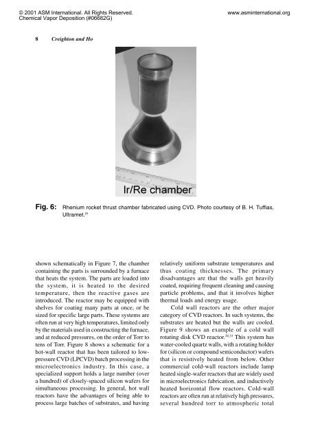
Fig. 6: Rhenium rocket thrust chamber fabricated using <strong>CVD</strong>. Pho<strong>to</strong> courtesy of B. H. Tuffias,<br />
Ultramet. 31<br />
shown schematically in Figure 7, the chamber<br />
containing the parts is surrounded by a furnace<br />
that heats the system. The parts are loaded in<strong>to</strong><br />
the system, it is heated <strong>to</strong> the desired<br />
temperature, then the reactive gases are<br />
introduced. The reac<strong>to</strong>r may be equipped with<br />
shelves for coating many parts at once, or be<br />
sized for specific large parts. These systems are<br />
often run at very high temperatures, limited only<br />
by the materials used in constructing the furnace,<br />
and at reduced pressures, on the order of Torr <strong>to</strong><br />
tens of Torr. Figure 8 shows a schematic for a<br />
hot-wall reac<strong>to</strong>r that has been tailored <strong>to</strong> lowpressure<br />
<strong>CVD</strong> (LP<strong>CVD</strong>) batch processing in the<br />
microelectronics industry. In this case, a<br />
specialized support holds a large number (over<br />
a hundred) of closely-spaced silicon wafers for<br />
simultaneous processing. In general, hot wall<br />
reac<strong>to</strong>rs have the advantages of being able <strong>to</strong><br />
process large batches of substrates, and having<br />
www.asminternational.org<br />
relatively uniform substrate temperatures and<br />
thus coating thicknesses. The primary<br />
disadvantages are that the walls get heavily<br />
coated, requiring frequent cleaning and causing<br />
particle problems, and that it involves higher<br />
thermal loads and energy usage.<br />
Cold wall reac<strong>to</strong>rs are the other major<br />
category of <strong>CVD</strong> reac<strong>to</strong>rs. In such systems, the<br />
substrates are heated but the walls are cooled.<br />
Figure 9 shows an example of a cold wall<br />
rotating disk <strong>CVD</strong> reac<strong>to</strong>r. 28,33 This system has<br />
water-cooled quartz walls, with a rotating holder<br />
for (silicon or compound semiconduc<strong>to</strong>r) wafers<br />
that is resistively heated from below. Other<br />
commercial cold-wall reac<strong>to</strong>rs include lamp<br />
heated single-wafer reac<strong>to</strong>rs that are widely used<br />
in microelectronics fabrication, and inductively<br />
heated horizontal flow reac<strong>to</strong>rs. Cold-wall<br />
reac<strong>to</strong>rs are often run at relatively high pressures,<br />
several hundred <strong>to</strong>rr <strong>to</strong> atmospheric <strong>to</strong>tal