

Chapter 1 Introduction to Chemical Vapor Deposition (CVD)
Chapter 1 Introduction to Chemical Vapor Deposition (CVD)
Chapter 1 Introduction to Chemical Vapor Deposition (CVD)

Create successful ePaper yourself
Turn your PDF publications into a flip-book with our unique Google optimized e-Paper software.
© 2001 ASM International. All Rights Reserved.<br />
<strong>Chemical</strong> <strong>Vapor</strong> <strong>Deposition</strong> (#06682G)<br />
often considered <strong>to</strong> be artificial a<strong>to</strong>ms, where<br />
the effect of quantum confinement significantly<br />
perturbs the normal bulk electronic properties<br />
of the material. One method of growing quantum<br />
dots involves depositing one material on another<br />
with a large lattice mismatch. The example in<br />
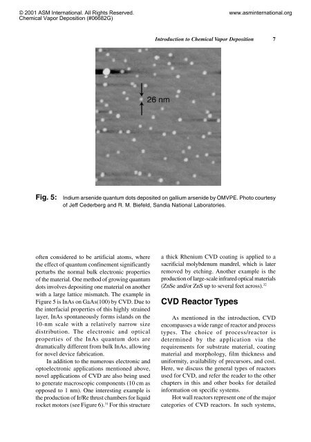
Figure 5 is InAs on GaAs(100) by <strong>CVD</strong>. Due <strong>to</strong><br />
the interfacial properties of this highly strained<br />
layer, InAs spontaneously forms islands on the<br />
10-nm scale with a relatively narrow size<br />
distribution. The electronic and optical<br />
properties of the InAs quantum dots are<br />
dramatically different from bulk InAs, allowing<br />
for novel device fabrication.<br />
In addition <strong>to</strong> the numerous electronic and<br />
op<strong>to</strong>electronic applications mentioned above,<br />
novel applications of <strong>CVD</strong> are also being used<br />
<strong>to</strong> generate macroscopic components (10 cm as<br />
opposed <strong>to</strong> 1 nm). One interesting example is<br />
the production of Ir/Re thrust chambers for liquid<br />
rocket mo<strong>to</strong>rs (see Figure 6). 31 For this structure<br />
<strong>Introduction</strong> <strong>to</strong> <strong>Chemical</strong> <strong>Vapor</strong> <strong>Deposition</strong> 7<br />
Fig. 5: Indium arsenide quantum dots deposited on gallium arsenide by OMVPE. Pho<strong>to</strong> courtesy<br />
of Jeff Cederberg and R. M. Biefeld, Sandia National Labora<strong>to</strong>ries.<br />
a thick Rhenium <strong>CVD</strong> coating is applied <strong>to</strong> a<br />
sacrificial molybdenum mandrel, which is later<br />
removed by etching. Another example is the<br />
production of large-scale infrared optical materials<br />
(ZnSe and/or ZnS up <strong>to</strong> several feet across). 32<br />
<strong>CVD</strong> Reac<strong>to</strong>r Types<br />
www.asminternational.org<br />
As mentioned in the introduction, <strong>CVD</strong><br />
encompasses a wide range of reac<strong>to</strong>r and process<br />
types. The choice of process/reac<strong>to</strong>r is<br />
determined by the application via the<br />
requirements for substrate material, coating<br />
material and morphology, film thickness and<br />
uniformity, availability of precursors, and cost.<br />
Here, we discuss the general types of reac<strong>to</strong>rs<br />
used for <strong>CVD</strong>, and refer the reader <strong>to</strong> the other<br />
chapters in this and other books for detailed<br />
information on specific systems.<br />
Hot wall reac<strong>to</strong>rs represent one of the major<br />
categories of <strong>CVD</strong> reac<strong>to</strong>rs. In such systems,