

Chapter 1 Introduction to Chemical Vapor Deposition (CVD)
Chapter 1 Introduction to Chemical Vapor Deposition (CVD)
Chapter 1 Introduction to Chemical Vapor Deposition (CVD)

Create successful ePaper yourself
Turn your PDF publications into a flip-book with our unique Google optimized e-Paper software.
© 2001 ASM International. All Rights Reserved.<br />
<strong>Chemical</strong> <strong>Vapor</strong> <strong>Deposition</strong> (#06682G)<br />
4<br />
Creigh<strong>to</strong>n and Ho<br />
refining of nickel, as developed by Mond,<br />
Langer, and Quincke in 1890. 19 Many of the<br />
early applications involved refining or<br />
purification of metals and a limited number of<br />
non-metals by carbonyl or halide processes.<br />
Other early applications involved deposition of<br />
coatings for wear and corrosion resistance, and<br />
the fabrication of structural shapes and<br />
components. Most of the earliest work, up <strong>to</strong><br />
the mid 1960s, is reviewed in the book by<br />
Powell, Oxley, and Blocher. 1 Many high volume<br />
applications, such as refining and the production<br />
of powders and pigments, are obviously still<br />
important economically, but most of the recent<br />
<strong>CVD</strong> R & D effort is aimed at thin-film<br />
deposition.<br />
There is a great deal of ongoing R & D<br />
regarding <strong>CVD</strong> of thin films used primarily for<br />
their mechanical or chemical properties. Many<br />
of these are discussed in detail in other chapters<br />
of this book, so we only briefly mention them<br />
here. <strong>Chapter</strong> 11 discusses the use of <strong>CVD</strong> films<br />
for tribological applications, chapter 13<br />
discusses <strong>CVD</strong> films used for corrosion<br />
protection, and chapter 14 discusses protective<br />
<strong>CVD</strong> coatings for <strong>to</strong>ol steels. <strong>Chapter</strong> 10<br />
discusses the <strong>CVD</strong> of diamond, and diamondlike<br />
carbon (DLC), which has generated a<br />
tremendous interest level in the past decade (see<br />
also last section, this chapter), and has significant<br />
commercial applications. Diamond films are<br />
mainly used for their hardness, but applications<br />
utilizing its high thermal conductivity, chemical<br />
inertness, or electronic properties are also<br />
important.<br />
A great deal of <strong>CVD</strong> R & D in recent<br />
decades, however, is focussed on the<br />
semiconduc<strong>to</strong>r revolution. We devote somewhat<br />
more space here <strong>to</strong> these applications, as they<br />
are not covered elsewhere in this book. <strong>CVD</strong><br />
has been a critical enabling technology in<br />
silicon-based microelectronics; it is even used<br />
at the earliest stage during the refining and<br />
purification of elemental silicon. Depending on<br />
the device, <strong>CVD</strong> processes are used for<br />
depositing thin films of the active semiconduc<strong>to</strong>r<br />
material (e.g. doped Si), conductive<br />
interconnects (e.g. tungsten), and/or insulating<br />
dielectrics (e.g. SiO 2 ), (see Figure 2).<br />
www.asminternational.org<br />
The communications revolution also relies<br />
on a diverse set of <strong>CVD</strong> technologies. Some<br />
components are similar <strong>to</strong> those used in silicon<br />
microelectronics, but many are unique, involving<br />
complex epitaxial heterostructures of SiGe or<br />
compound semiconduc<strong>to</strong>r (e.g., AlGaAs) alloys<br />
that are required <strong>to</strong> yield high frequency (1-100<br />
GHz) device operation. 20 The communication<br />
revolution also relies on op<strong>to</strong>electronic<br />
components, such as solid state diode lasers<br />
(another complex heterostructure device), and<br />
these devices are often grown by <strong>CVD</strong>. 7,21 Even<br />
the fiberoptic cables that transmit the optical<br />
component of the communications network are<br />
manufactured using a <strong>CVD</strong> technique <strong>to</strong> achieve<br />
the desired refractive index profile. 22<br />
Op<strong>to</strong>electronic material grown by <strong>CVD</strong> has<br />
many applications outside of the<br />
communications industry. One example is for<br />
solid state lighting using light emitting diodes<br />
(LEDs). Recently, Nichia <strong>Chemical</strong> was the first<br />
company <strong>to</strong> commercialize high brightness blue<br />
and green LEDs based on group-III nitride<br />
alloys, e.g. InGaN, which are grown on sapphire<br />
substrates using <strong>CVD</strong> technology. 23 This<br />
company also introduced the first long-life blue<br />
laser diode, based on the same material and<br />
technology. In addition <strong>to</strong> the myriad of lighting<br />
and signage applications using colored LEDs,<br />
there is a growing interest in generating solid<br />
state white light sources <strong>to</strong> replace incandescent<br />
and perhaps even fluorescent sources. 24 A solidstate<br />
white light source may be achieved by<br />
combining LEDs of different wavelengths, or<br />
by pumping a phosphor with an ultraviolet LED.<br />
Another exciting technology utilizing <strong>CVD</strong><br />
is the production of microelectromechanical<br />
structures, or MEMS. 25 Much of the MEMS<br />
technology is derived from the silicon<br />
microelectronics technology, so it is not<br />
surprising that <strong>CVD</strong> plays a crucial role. Most<br />
MEMS devices are fabricated from<br />
polycrystalline silicon (polysilicon) films<br />
deposited on silicon wafers, with intermediate<br />
sacrificial SiO 2 layers that are later removed by<br />
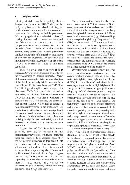
chemical etching. Figure 3 shows an example<br />
of such a device, in this case a set of interlocking<br />
gears that are ~50-200 microns in diameter. Both<br />
the polysilicon and oxide are deposited using