OEM spectro Catalogue - Horiba
OEM spectro Catalogue - Horiba
OEM spectro Catalogue - Horiba

You also want an ePaper? Increase the reach of your titles
YUMPU automatically turns print PDFs into web optimized ePapers that Google loves.
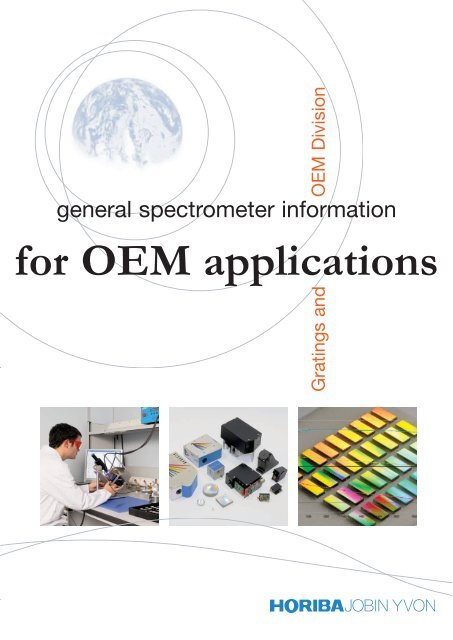
Gratings and <strong>OEM</strong> Division<br />
general <strong>spectro</strong>meter information<br />
for <strong>OEM</strong> applications
2<br />
Commitment to quality<br />
HORIBA Jobin Yvon offers complete customer service,<br />
including expert technical advice for optimizing system<br />
configurations to meet customers’ needs.<br />
HORIBA Jobin Yvon is ISO 9001:2000 certified,<br />
and our well-staffed departments are committed to customer<br />
satisfaction and product quality.<br />
HORIBA Jobin Yvon attempts to provide accurate information<br />
in this catalogue, however HORIBA Jobin Yvon<br />
assumes no responsibility should errors or inaccuracies<br />
occur. HORIBA Jobin Yvon reserves the right to change the<br />
content without notice and provides this catalog "as is" with<br />
no warranty either express or implied.
Introduction<br />
As a pioneer and world leader in the field of diffraction<br />
gratings, HORIBA Jobin Yvon continues<br />
to develop advanced manufacturing processes<br />
for industrial and scientific applications.<br />
Founded in 1819, HORIBA Jobin Yvon has defined<br />
the leading edge of optics for<br />
<strong>spectro</strong>scopy for over 180 years. Our<br />
leadership in optics has been<br />
demonstrated by the continuing<br />
development of both ruled and holographic<br />
grating technology, including<br />
the invention of aberration-corrected<br />
holographic gratings and ion-etched<br />
blazed holographic gratings.<br />
HORIBA Jobin Yvon is a specialist in<br />
<strong>spectro</strong>meters, illumination systems<br />
and detectors. Our daily business is<br />
the development of <strong>spectro</strong>meter<br />
systems for industrial applications.<br />
Our high volume replicated gratings<br />
and optical modules are used in many instruments<br />
such as <strong>spectro</strong>photometers, bioanalysers,<br />
colorimeters, etc.<br />
HORIBA Jobin Yvon’s gratings for scientific<br />
applications can be found in our scientific diffraction<br />
grating catalog.<br />
Contact your HJY representative for assistance with<br />
choosing the right grating for your application.<br />
Visit our website: www.jobinyvon.com<br />
3
4<br />
Introduction<br />
. . . . . . . . . . . . . . . . . . . . . . . . . . . . . . . . . . . . . . . . . . . . . . . . . . . . . . . . . . . . . .3<br />
Spectrometers for <strong>OEM</strong> applications<br />
. . . . . . . . . . . . . . . . . . . . . . . . . . . . . . . . . . . . . . . . .5<br />
Performance criteria for the choice of compact <strong>spectro</strong>meters<br />
. . . . . . . . . . . . . . . . . . .6<br />
State of the art <strong>OEM</strong> solutions . . . . . . . . . . . . . . . . . . . . . . . . . . . . . . . . . . . . . . . . . . . . . .12<br />
Existing proof of concept systems . . . . . . . . . . . . . . . . . . . . . . . . . . . . . . . . . . . . .13<br />
Spectro-cube . . . . . . . . . . . . . . . . . . . . . . . . . . . . . . . . . . . . . . . . . . . . . . . . .14<br />
VS70-M . . . . . . . . . . . . . . . . . . . . . . . . . . . . . . . . . . . . . . . . . . . . . . . . . . . . . .15<br />
VS140-M . . . . . . . . . . . . . . . . . . . . . . . . . . . . . . . . . . . . . . . . . . . . . . . . . . . . .17<br />
Modular <strong>spectro</strong>scopy components . . . . . . . . . . . . . . . . . . . . . . . . . . . . . . . . . . . .19<br />
Miniature <strong>spectro</strong>graphs: the CP family . . . . . . . . . . . . . . . . . . . . . . . . . . . .20<br />
Compact <strong>spectro</strong>graphs: the VS family . . . . . . . . . . . . . . . . . . . . . . . . . . . . .22<br />
Imaging compact <strong>spectro</strong>graphs . . . . . . . . . . . . . . . . . . . . . . . . . . . . . . . . . .27<br />
Spectrometer comparaison chart . . . . . . . . . . . . . . . . . . . . . . . . . . . . . . . . . .29<br />
Compact scanning monochromators . . . . . . . . . . . . . . . . . . . . . . . . . . . . . . .30<br />
H10-34B <strong>OEM</strong> imaging monochromator . . . . . . . . . . . . . . . . . . . . . .31<br />
H10-61 <strong>OEM</strong> monochromator . . . . . . . . . . . . . . . . . . . . . . . . . . . . . .33<br />
Basic definitions . . . . . . . . . . . . . . . . . . . . . . . . . . . . . . . . . . . . . . . . . . . . . . . . . . . . . . . . .35<br />
Information request form . . . . . . . . . . . . . . . . . . . . . . . . . . . . . . . . . . . . . . . . . . . . . . . . . .43<br />
www.jobinyvon.com
Spectrometers for <strong>OEM</strong> applications<br />
The market growth of miniature and compact <strong>spectro</strong>meters has<br />
been a significant development in recent years, and more particularly<br />
in <strong>OEM</strong> applications.<br />
Miniaturization, robustness, cost reductions, and improvements in<br />
the performance of array detectors have allowed the use of these<br />
sensors in many industrial applications.<br />
These <strong>spectro</strong>meters that operate from the UV to the near infrared<br />
range of the spectrum are used in many applications such as:<br />
o Color measurement<br />
o Analytical chemistry<br />
o Biomedical<br />
o Fluorescence<br />
o Raman<br />
o Elemental analysis<br />
With more than 20 years of <strong>OEM</strong> experience in the <strong>spectro</strong>scopy<br />
market, HORIBA Jobin Yvon has taken a strong position worldwide.<br />
Our <strong>spectro</strong>meters and diffraction gratings have been selected<br />
by <strong>OEM</strong> customers because they offer higher optical performance,<br />
such as superior signal to noise ratio, high throughput,<br />
aberration correction, and robust single optic design.<br />
The first part of this document will help you to deal with important<br />
criteria for the choice of <strong>spectro</strong>meters. The second part introduces<br />
existing <strong>OEM</strong> proof of concept systems to help customers<br />
to validate specifications.<br />
Then, we present a broad selection of modular components, such<br />
as miniature and compact <strong>spectro</strong>graphs, detectors, electronic<br />
drivers, light sources, etc..<br />
These components can be used for prototype purposes and final<br />
products.<br />
In the last section, we offer some basic definitions related to <strong>spectro</strong>meters.<br />
H10-34<br />
VS70<br />
CP20<br />
VS70 and <strong>spectro</strong>-cube<br />
Concave gratings<br />
5
6<br />
Performance criteria for the choice of<br />
compact <strong>spectro</strong>meters<br />
The performance of <strong>spectro</strong>meters is judged by three criteria:<br />
o System resolution<br />
o Throughput<br />
o System limit of detection<br />
These criteria are effected by the grating efficiency, system light<br />
collection capability, system stray light and design aberrations.<br />
Each of these design criteria is described hereafter.<br />
Grating efficiency:<br />
Holographic gratings are available with three different groove profiles.<br />
Each of these profiles has different efficiency advantages.<br />
Figures 1, 2, and 3 show the sinusoidal, laminar and triangular<br />
groove profile, respectively.<br />
The maximum theoretical average efficiency (of unpolarized light)<br />
of the sinusoidal grating profile is around 35%.<br />
Laminar and triangular groove profiles are produced with an ion<br />
etching process that shapes the groove profile.<br />
The laminar profile grating improves the efficiency, but the main<br />
advantage of this profile is the reduction in second order efficiency.<br />
The second order is reduced to as low as 0.4%.<br />
The triangular groove profile has efficiency profiles similar to ruled<br />
gratings. Peak efficiencies of 50% to 70% are possible.<br />
pseudo sinusoidal profile<br />
laminar profile<br />
a = groove spacing<br />
h = modulation depth<br />
Figure 1: sinusoidal groove profile<br />
c<br />
h<br />
d<br />
c<br />
d<br />
c/d = groove width to groove<br />
spacing ratio<br />
h = groove depth<br />
Figure 2: laminar groove profile<br />
a = blaze angle<br />
Figure 3: triangular groove profile<br />
Holographic sinusoidal efficiency Holographic laminar efficiency Holographic triangular efficiency<br />
h<br />
triangular profile
System light collection<br />
capability<br />
Concave aberration corrected grating instruments<br />
are defined by the grating. Concave gratings<br />
are described by their arm lengths and<br />
included angle. The grating is the sole optical<br />
element in this design. The system light collection<br />
is determined by the f-number (f/#) of the<br />
grating. The f-number is the ratio of the grating<br />
focal length divided by the grating diameter<br />
(clear aperture). A lower f/# indicates a greater<br />
ability to gather light.<br />
Aberration correction allows higher light collection<br />
compared with standard commercial <strong>spectro</strong>meter<br />
designs.<br />
Concave grating <strong>spectro</strong>meter designs with fnumbers<br />
of f/2 and faster (toward f/1.5) are common.<br />
By comparison, most retail instruments<br />
from competition use plane grating designs and<br />
operate at f-numbers between f/3 and f/10.<br />
Aberration correction allows a <strong>spectro</strong>meter to<br />
operate at low f-number because of the reduction<br />
in the effects of aberrations. Low f-number<br />
designs, possible with concave gratings, offer<br />
the advantage of increased light collection capability<br />
over plane grating designs. Light collection<br />
F: grating focal length - D: grating diameter<br />
capability comparisons of instruments can be<br />
done by taking the ratio of the squares of the<br />
design f-numbers. To compare the collection<br />
ability of a f/5 plane grating design instrument<br />
and a f/2 concave grating design, calculate the<br />
ratio of 5² to 2², or 25 to 4.<br />
The light collection of f/2 concave grating design<br />
is more than six times greater than the equivalent<br />
f/5 design. The system collection efficiency is<br />
optimized with concave gratings while providing<br />
a simple, cost-effective design. Additional mirrors<br />
and mirror mounts are not necessary in<br />
these designs, making them more robust and<br />
intrinsically providing a better signal to noise<br />
ratio.<br />
System stray light<br />
The process of manufacturing holographic gratings<br />
has many advantages compared with ruled<br />
gratings for stray light rejection.<br />
First, it provides a better periodicity of the<br />
grooves that can not be achieved with a ruled<br />
grating. Additionally, it makes the grating surface<br />
smoother than ruled gratings. Surface roughness<br />
is a significant source of grating generated stray<br />
light (see picture below). It is important to<br />
remember that everything scatters light.<br />
ruled diffraction grating<br />
holographic diffraction grating<br />
7
8<br />
All gratings exhibit some amount of scattered<br />
light. The inherently lower scatter of holographic<br />
gratings improves the system performance.<br />
Concave grating designs have two additional<br />
design advantages, with respect to system stray<br />
light, over most commercial plane grating designs.<br />
First, grating scatter in Czerny Turner and<br />
Fastie Ebert designs is collected and focused,<br />
by the focusing mirror, toward the exit port. In<br />
concave grating designs the grating does not<br />
focus its own scattered light into the focal plane.<br />
Secondly, rediffracted light is minimized.<br />
Rediffracted light is light that is diffracted by the<br />
grating and redirected back to the grating a<br />
second time (unintentionally of course).<br />
When other concave optics (collimating and<br />
focusing mirrors) are used in an instrument design<br />
it is more likely that light may be rediffracted.<br />
Careful design effort is necessary to prevent<br />
rediffracted light.<br />
Concave gratings are immune from this problem<br />
when working at f-numbers greater than f/2 with<br />
low groove density (< 600 gr/mm) gratings.<br />
point<br />
spherical<br />
aberration<br />
optical<br />
coma<br />
system<br />
point<br />
astigmatism<br />
spot diagrams from a point<br />
chromatic<br />
aberration<br />
optical<br />
system<br />
spot diagrams from a point<br />
Aberration correction<br />
Aberration correction is the most important<br />
benefit of concave aberration corrected holographic<br />
gratings.<br />
To understand the benefit of aberration correction<br />
it is important to understand the main aberrations<br />
in <strong>spectro</strong>meter designs and their impact<br />
on system results.<br />
Optical components can create errors in an<br />
image even if they are made of the best materials<br />
and have no defects. These aberrations can be<br />
grouped into several different categories: spherical<br />
aberration, coma, astigmatism, and field curvature.<br />
The effects of coma, spherical aberration, astigmatism<br />
and field curvature can cause degradation<br />
of the system’s performance. Some description<br />
is necessary for how these aberrations relate<br />
to the exit focal plane of a <strong>spectro</strong>meter.<br />
coma<br />
chromatic<br />
aberration<br />
spherical<br />
aberration<br />
astigmatism
Spherical aberration (SA)<br />
Spherical aberrations result from the fact that the focal points of<br />
light rays far from the optic axis of a spherical lens or mirror are different<br />
from the focal points of rays of the same wavelength passing<br />
near the center.<br />
A spherical mirror does not precisely focus a point to a point. As<br />
light rays move further away from the center axis of a mirror, the<br />
focal point moves closer to the mirror. A zone of confusion is created<br />
in the image plane because of the changing focal point with<br />
distance from center axis. This “zone” of confusion prevents the<br />
ability to obtain a sharp focused image. SA is difficult to eliminate<br />
without the use of aspheric optics.<br />
The result of SA is loss of resolution. Imaging performance<br />
degrades causing crosstalk from adjacent wavelengths. In aberration<br />
corrected designs the concave grating is designed to correct<br />
SA.<br />
Coma is an aberration resulting from using off axis optics. Coma<br />
causes an unsymmetrical spectral line broadening. This broadening<br />
leads to resolution losses and stray light. On a detector array,<br />
the impact is pixel to pixel crosstalk and loss of resolution.<br />
Coma can be corrected in some instruments, at one wavelength,<br />
by adjusting the optical geometry.<br />
Coma can be corrected at many wavelengths in the concave aberration<br />
corrected grating design.<br />
Astigmatism (AST) is another aberration resulting from the use<br />
of off axis optics. Point sources “grow” in height as the longitudinal<br />
astigmatism increases. Longitudinal astigmatism is the result of<br />
the tangential and sagittal components focusing in different planes.<br />
Astigmatism effects can lead to a 400 micron input fiber (at the<br />
input slit position) “growing” to 2 millimeters high at the output<br />
focal plane. When using a 0.5 millimeter high array, and the exit<br />
focal plane image is 2 millimeters, 75% of the output signal is not<br />
measured. This effect leads to loss of system throughput and the<br />
limit of detection.<br />
b<br />
Optical system without (a) and<br />
with (b) spherical aberrations.<br />
Spherical aberration is caused by<br />
different focal points for rays far<br />
from the center and others closer<br />
to it (b).<br />
a<br />
9
10<br />
To illustrate the possibilities of concave aberration corrected grating<br />
designs, the figure below shows the performance of a concave aberration<br />
corrected grating design compared with that of Czerny-Turner design without<br />
astigmatism correction.<br />
Here, spot diagrams for an f/2 CP140 aberration corrected <strong>spectro</strong>graph are compared to those from an equivalent focal<br />
length Czerny-Turner <strong>spectro</strong>graph (“CZT140”, f=140 mm) at f/4.<br />
The input slit size in both instruments was set to 0.20 mm (W)x0.5 mm (H). The CP140 optimally images at all wavelengths,<br />
whereas the CZT140 produces a very tall image. As the wavelength increases, the degree of astigmatism in the Czerny-<br />
Turner design also increases, resulting in a decrease of flux density due to the increasing image height.<br />
The fast f/2 CP140 has a much higher light gathering capacity compared to the CZT140 at f/4.<br />
Thus the effective flux density of signal from the aberration corrected CP140 is almost 40 times higher than that from the<br />
equivalent Czerny-Turner instrument.<br />
H1034 scanning <strong>spectro</strong>meter spot diagrams<br />
SPOT DIAGRAM INSTRUMENTAL PROFILE SPOT DIAGRAM INSTRUMENTAL PROFILE<br />
l = 250 nm<br />
bandpass (FWHM) = 2 nm<br />
*TH = 93.1 P.C.<br />
dispersion = 6.2 nm/mm<br />
*TH : rate of the useful ligth limited by the height of the exit slit (or pixel).<br />
CZT140<br />
l = 750 nm<br />
bandpass (FWHM) = 2 nm<br />
TH = 95.5 P.C.<br />
dispersion = 7.2 nm/mm<br />
This figure shows spot diagrams of the H1034, 100 millimeter focal length, scanning <strong>spectro</strong>meter. This instrument<br />
uses a 1200 grooves per millimeter concave aberration corrected f/3 grating. The 250 nanometer to 750<br />
nanometer wavelength range is very well corrected for coma, SA, AST and field curvature.
Field curvature (FC) is the shape of the image<br />
plane (usually called the Petzval Field). The<br />
shape of the field determines the shape of<br />
images at the exit. Field curvature can cause<br />
calibration errors for off-axis sources and pixel to<br />
pixel crosstalk on arrays. Calibration errors and<br />
increased blur of off-axis inputs are considered<br />
stray light. Aberration corrected gratings can<br />
change the shape of the exit focal plane field.<br />
Aberration corrected gratings are often called<br />
“flat field” gratings. This feature prevents image<br />
degradation for off axis images. Designs without<br />
this correction often suffer from spatial and<br />
spectral resolution losses for off axis inputs.<br />
Aberration conclusion review<br />
Coma, SA, and FC contribute to near end stray<br />
light (light from adjacent wavelengths). Light that<br />
does not properly strike the detector decreases<br />
the system performance.<br />
The signal to noise ratio suffers because of low<br />
throughput per pixel and increased pixel to pixel<br />
crosstalk.<br />
Putting the advantages of efficiency, system light<br />
collection capability, system stray light advantages<br />
and aberration correction together provides<br />
a clear view of the advantages of the holographic<br />
concave aberration corrected grating<br />
designs. The performance advantages of aberration<br />
corrected concave gratings, together with<br />
the simple, compact and robust design optimize<br />
system performance<br />
Technology pushing instrument design<br />
In the past three decades detector technology<br />
has progressed from film to phototubes to photodiode<br />
arrays to charge coupled devices<br />
(CCDs). The use of small diameter optical fibers<br />
(with high numerical apertures) coupled with new<br />
detector technology has made improving imaging<br />
performance of existing instruments much<br />
more important.<br />
Good off axis performance has become necessary<br />
as applications using fiber arrays and tall<br />
CCD arrays are used together in applications. It<br />
is in this area that aberration corrected holographic<br />
grating designs have made the biggest<br />
impact. Aberrations such as coma, spherical<br />
aberration, astigmatism and field curvature make<br />
point to point imaging a difficult challenge.<br />
Commercially available instruments are designed<br />
as all-purpose instruments. They must<br />
adapt to applications that work well in the UV<br />
through the far infrared in scanning and image<br />
modes. For dedicated industrial applications, a<br />
more specific design can lead to an instrument<br />
that outperforms the all-purpose, one size fits all,<br />
instrument design.<br />
For those users with dedicated, repetitive applications<br />
(as with most <strong>OEM</strong> grating customers),<br />
<strong>spectro</strong>meters with concave gratings are the<br />
obvious choice. Another advantage of aberration<br />
correction gratings well worth mentioning is the<br />
ability to correct for aberrations in other parts of<br />
the optical system.<br />
Other system aberrations (e.g., aberrations from<br />
lenses, mirrors or sample-related problems) can<br />
be corrected with an appropriate grating design.<br />
The concave aberration corrected grating design<br />
can incorporate the required corrections for system<br />
coma, spherical aberration, astigmatism and<br />
field curvature.<br />
This system design approach can improve resolution<br />
and spatial imaging. Design success will<br />
often depend on achieving the optimal coupling<br />
of all system components.<br />
Aberration corrected holographic grating designs<br />
are used in many industrial systems to<br />
optimize throughput while reducing noise.<br />
11
12<br />
State of the art <strong>OEM</strong> solutions<br />
Existing proof of concept systems<br />
Modular <strong>spectro</strong>scopy components
Existing proof of concept systems<br />
This new line of modules is an example of how HORIBA Jobin<br />
Yvon can supply <strong>spectro</strong>scopy solutions which are suitable<br />
for a wide range of applications.<br />
These modules are exclusively available to help<br />
<strong>OEM</strong> customers quickly define important performance<br />
parameters, after which a fully customized<br />
<strong>spectro</strong>scopy solution can be achieved.<br />
They have been specially developed with the main<br />
goal of significantly reducing <strong>OEM</strong>'s development<br />
time.<br />
<strong>OEM</strong> customers can take advantage of our <strong>spectro</strong>scopic<br />
expe-rience and become our next industrial partner for their<br />
next project.<br />
These rugged and compact modules, designed around a family of<br />
aberration corrected holographic concave gratings which maximize<br />
optical performance and minimize the stray light, feature a<br />
high efficiency level, the largest aperture in their class, and a large<br />
choice of spectral ranges.<br />
Available with a choice of linear array detectors, these modules<br />
can be equipped either with linear CCD detectors for high sensitivity<br />
or with a photodiode array, ensuring a wide dynamic range and<br />
a high signal to noise ratio when coupled with a 16 bit A/D converter.<br />
These fully packaged systems are built around the modular<br />
components described in the next section.<br />
The following table outlines the proof of concept systems and their<br />
constituent <strong>spectro</strong>graphs:<br />
Proof of concept systems See page Constituent Spectrographs See page<br />
SPECTRO-CUBE 14 CP20<br />
(Miniature <strong>spectro</strong>graph)<br />
VS70-M 15 VS70<br />
(Compact <strong>spectro</strong>graph)<br />
VS140-M 17 VS140<br />
(Compact <strong>spectro</strong>graph)<br />
Applications<br />
o Colorimetry<br />
o Life science<br />
o Analytical chemistry<br />
o Process monitoring<br />
o and many others<br />
Three modules are<br />
currently available:<br />
o Spectro-cube<br />
o VS70-M<br />
o VS140-M<br />
20<br />
22<br />
22<br />
13
14<br />
SPECTRO-CUBE<br />
Designed around the miniature CP20 <strong>spectro</strong>graph, the <strong>spectro</strong>cube<br />
is a plug & play module that can be customized for a variety<br />
of <strong>OEM</strong> applications such as color measurement, life science,<br />
process monitoring, etc.<br />
The <strong>spectro</strong>-cube is available in 2 versions:<br />
o <strong>spectro</strong>-cube-T<br />
o <strong>spectro</strong>-cube-H<br />
Tungsten Halogen spectrum<br />
Signal<br />
Specifications<br />
wavelength (nm)<br />
Features<br />
o Compact, for hand-held<br />
instruments<br />
o Low stray light<br />
o Superb imaging properties<br />
o Reliable<br />
o Robust<br />
SPECTRO-CUBE-T SPECTRO-CUBE-H<br />
optical<br />
optical bench design CP20<br />
wavelegth range 350-900 nm 380-760 nm<br />
aperture (f/#) 2.7<br />
average dispersion* 65 nm/mm<br />
stray light < 0.1% at 415 nm with RG630<br />
entrance aperture 50, 100, 250 µm wide slits or fiber<br />
fiber optic connector SMA 905<br />
wavelength accuracy < 0.5 nm (with a mathematical fit) < 0.5 nm (with a mathematical fit)<br />
wavelength reproducibility<br />
electronic<br />
< 0.1 nm < 0.1 nm<br />
detector CMOS linear sensor array (TAOS) CMOS linear PDA (HAM...)<br />
number of pixels 128 pixels 128 or 256 pixels<br />
pixel width 55.5 µm 25 or 50 µm<br />
pixel height 63.5 µm 500 µm<br />
signal to noise 300:1 (at full signal) 2500:1 (at full dynamic)<br />
A/D resolution 14 bit<br />
computer interfaces USB<br />
operating systems<br />
physical<br />
Windows 98/ME/2000/XP<br />
dimensions (mm) 50x50x50 mm<br />
power supply USB powered<br />
*For example : the optical resolution with a slit or fiber of 50 µm width is around 5 nm
VS70-M<br />
The VS70-M is a plug and play evaluation<br />
module that is exclusively available to help<br />
<strong>OEM</strong> customers quickly define important performance<br />
parameters, after which a fully customized<br />
<strong>spectro</strong>scopy solution can be achieved.<br />
Designed around the versatile VS70 <strong>spectro</strong>graph, this high performance<br />
module can be used for a variety of <strong>OEM</strong> applications:<br />
o Colorimetry<br />
o Analytical chemistry<br />
o Life science<br />
o Process monitoring<br />
o and many others<br />
The VS70-M is aligned, wavelength calibrated and tested at the<br />
factory in accordance with your requirements, ensuring consistently<br />
high performance.<br />
Connect the VS70-M to your USB interface and take data immediately.<br />
The VS70-M is currently available in two versions:<br />
o VS70-M-CCD<br />
o VS70-M-PDA<br />
VS70-M-CCD<br />
This version is suggested for applications when sensitivity is<br />
needed. It is based on a VS70 equipped with a linear CCD array.<br />
VS70-M-PDA<br />
For applications where high dynamic range is a premium, the<br />
VS70-M-PDA is preferable. It is based on a VS70 equipped with a<br />
linear PDA.<br />
Features<br />
o Plug and play module<br />
Just plug the USB connection<br />
to the 16 bit electronic driver<br />
and start your measurements<br />
o Integrated <strong>spectro</strong>scopy<br />
module<br />
Ready for integration into<br />
<strong>OEM</strong> instruments<br />
o UV to NIR range<br />
One grating to cover<br />
190-1050 nm<br />
o High optical performance<br />
High thoughput (f/2 optic)<br />
Resolution < 2 nm<br />
Stray light < 10 -3<br />
o High sensitivity and<br />
dynamic range<br />
CCD and PDA detectors<br />
ensure high sensitivity and<br />
high dynamic range<br />
o Internally stored wavelength<br />
calibration coefficients<br />
Calibration done at factory<br />
o Compact size<br />
Easy to integrate in a variety<br />
of instruments<br />
o Flexibility and robustness<br />
Safe and simple optical design;<br />
custom <strong>OEM</strong> design possible<br />
o SMA fiber optic interface<br />
Standard SMA interface simplifies<br />
compatibility<br />
15
16<br />
Specifications<br />
VS70-M-CCD-BT VS70-M-CCD VS70-M-PDA/C VS70-M-PDA/N<br />
optical<br />
optical bench design VS70<br />
wavelength ranges from 190-1050**<br />
aperture (f/#) 2<br />
average dispersions* 17 nm/mm; 23 nm/mm; 33 nm/mm<br />
entrance aperture 50,100,250 µm wide slits or fiber<br />
fiber optic connector SMA 905<br />
order sorting filter yes<br />
wavelength accuracy < 0.5 nm (with a mathematical fit)<br />
wavelength reproducibility<br />
electronic<br />
< 0.1 nm<br />
detector back thinned CCD linear CCD array CMOS PDA<br />
array S9840 (Ham.)<br />
TCD 1304 (Tosh.)<br />
S83xx (Ham.)<br />
NMOS PDA<br />
S39xx (Ham.)<br />
number of pixels 2048 pixels 3648 pixels 512 or 1024 pixels<br />
pixel width 14 µm 8 µm 25 or 50 µm<br />
pixel height 200 µm 500 or 2500 µm height<br />
signal to noise*** 1000:1 300:1 3500:1 6000:1<br />
A/D resolution 16 bit<br />
computer Interfaces USB/RS232<br />
operating systems Windows 98/ME/2000/XP<br />
physical<br />
dimensions 90x110x49 mm<br />
weight 500 g<br />
* depending on the grating. For example: with an average dispersion grating of 17 nm/mm, the optical resolution with a slit<br />
or fiber of 50 µm width is around 1 nm<br />
** depending on the grating and on the position of the array<br />
*** at full signal<br />
This module comes with Windows-based software which includes basic<br />
functions like dark subtraction, reference, absorbance, etc. as well as an<br />
Excel link. In addition a set of DLLs or software development kit (SDK) is<br />
available to help customers develop their own application software.<br />
Software Features<br />
o real time<br />
%T, AU, spectral -+/,log<br />
o real-time data smoothing<br />
o real-time data transfer to Excel<br />
o automated acquisition with time<br />
o stamped file names<br />
o external triggering<br />
o polynomial fit wavelength<br />
linearization<br />
o user notes with automated acquisition<br />
parameters insertion<br />
These two spectra have been measured<br />
with different integration times
VS140-M<br />
The VS140-M is a plug and play evaluation<br />
system that is available to help <strong>OEM</strong> customers<br />
during proof of concept phase, to<br />
define important performance parameters,<br />
after which a fully customized <strong>spectro</strong>scopy<br />
solution can be achieved.<br />
Designed around the versatile VS140 <strong>spectro</strong>graph, this high performance<br />
module can be customized for a variety of <strong>OEM</strong> applications:<br />
o Colorimetry<br />
o Analytical chemistry<br />
o Life science<br />
o Process monitoring<br />
o and many others<br />
The VS140-M is aligned, wavelength calibrated and tested at the<br />
factory in accordance with your requirements, ensuring consistently<br />
high performance.<br />
Connect the VS140-M to your USB interface and take data immediately.<br />
The VS140-M is currently available in three versions:<br />
o VS140-M-CCD<br />
o VS140-M-PDA<br />
o VS140-M-INGAAS<br />
VS140-M-CCD<br />
This version is suggested for applications where sensitivity is<br />
needed. It is based on a VS140 equipped with a linear CCD array.<br />
VS140-M-PDA<br />
For applications where high dynamic range is a premium, the<br />
VS140-M-PDA is preferable. It is based on a VS140 equipped with<br />
a linear PDA.<br />
VS140-M-INGAAS<br />
For applications in the NIR range, the VS140-M-INGAAS is<br />
obvious choice. It is based on a VS140 equipped with a InGaAs<br />
linear array detector.<br />
Features<br />
o Plug and play module<br />
Just plug the USB connection<br />
to the 16 bit electronic driver<br />
and start your measurements<br />
o Integrated <strong>spectro</strong>scopy<br />
module<br />
Ready for integration into<br />
<strong>OEM</strong> instruments<br />
o UV to NIR range<br />
Large selection of gratings to<br />
cover from 190 to 2500 nm<br />
o High optical performance<br />
High thoughput (f/#2 optic)<br />
Resolution � 1 nm<br />
Stray light < 10 -3<br />
o High sensitivity and<br />
dynamic range<br />
CCD and PDA detectors<br />
ensure high sensitivity and<br />
high dynamic range<br />
o Internally stored wavelength<br />
calibration coefficients<br />
Calibration done at factory<br />
o Compact size<br />
Easy to integrate in a variety<br />
of instruments<br />
o Flexibility and robustness<br />
Safe and simple optical design;<br />
Custom <strong>OEM</strong> design possible<br />
o SMA fiber optic interface<br />
Standard SMA interface simplifies<br />
compatibility<br />
17
18<br />
Specifications<br />
VS140-M-CCD-BT VS140-M-PDA VS140-M-PDA VS140-M-INGAAS<br />
optical<br />
optical bench design VS140<br />
wavelength ranges from 190-1050 nm** from 800-1700 nm**<br />
aperture (f/#) 2.4<br />
average dispersions 17 nm/mm; 24 nm/mm; 30 nm/mm 70 nm/mm<br />
entrance aperture 25, 50, 100, 250 µm wide slits or fiber<br />
fiber optic connector SMA 905<br />
order sorting filter yes yes yes no<br />
wavelength accuracy < 0.5 nm (with a mathematical fit)<br />
wavelength<br />
reproducibility<br />
electronic<br />
< 0.1 nm<br />
detector<br />
back thinned CCD array<br />
S9840<br />
CMOS S83xx<br />
linear photodiode array<br />
NMOS S39xx<br />
linear photodiode array<br />
INGAAS<br />
linear photodiode array<br />
number of pixels 14 lines of 2048 pixels 512 or 1024 pixels 512 or 1024 pixels 256 pixels<br />
pixel width 14 µm 25 or 50 µm 25 or 50 µm 25 or 50 µm<br />
pixel height 200 µm 500 or 2500 µm height 500 or 2500 µm height 500 or 2500 µm height<br />
signal to noise*** 1000:1 3500:1 6000:1 6000:1<br />
A/D resolution 16 bit<br />
computer Interfaces USB/RS232<br />
operating systems<br />
physical<br />
Windows 98/ME/2000/XP<br />
dimensions 120x150x110 mm<br />
weight 900 g<br />
* depending on the grating. For example: with an average dispersion grating of 17 nm/mm, the optical resolution with a slit<br />
or fiber of 50 µm width is around 1 nm<br />
** depending on the grating and on the position of the array<br />
*** at full signal<br />
This module comes with Windows based software which includes basic<br />
functions like dark subtraction, reference, absorbance, etc. as well as an<br />
Excel link. In addition a set of DLLs drivers or a software development kit<br />
(SDK) is available to help customers develop their own application<br />
software.<br />
Software Features<br />
o real time<br />
%T, AU, spectral -+/,math log<br />
o real-time data smoothing<br />
o real-time data transfer to Excel<br />
o automated acquisition with time<br />
o stamped file names<br />
o external triggering<br />
o polynomial fit wavelength<br />
linearization<br />
o user notes with automated acquisition<br />
parameters insertion<br />
These two spectra have been measured<br />
with different integration times
Modular <strong>spectro</strong>scopy components<br />
a starting point for rapid prototypes<br />
HORIBA Jobin Yvon’s miniature & compact <strong>spectro</strong>graphs can be<br />
customized for most major <strong>spectro</strong>scopy applications of Original<br />
Equipment Manufacturers (<strong>OEM</strong>s).<br />
Available from ultraviolet to infrared, these <strong>spectro</strong>graphs are compact<br />
with focal lengths ranging from 20 mm to 140 mm.<br />
These versatile <strong>spectro</strong>graphs use aberration corrected high efficiency<br />
concave holographic gratings.<br />
HORIBA Jobin Yvon manufactures a wide variety of high performance<br />
diffraction gratings for these <strong>spectro</strong>graphs configured for<br />
spectral regions from 190 to 2500 nm.<br />
The optical <strong>spectro</strong>meter design consists of a fixed input slit with<br />
fiber adapter, an aberration corrected concave grating and a linear<br />
or 2-D array with electronics. The whole set is assembled into a<br />
rugged and compact housing.<br />
The design is optimized to produce well focused spectra over a<br />
long flat focal plane making it ideal for photodiode arrays, linear<br />
CCDs or 2 dimensional CCDs.<br />
Applications include color monitoring, food inspection, petrochemical<br />
analysis, clinical chemistry, radiometry, chromatography<br />
detection, plasma monitoring, pollution detection, etc.<br />
CP20, CP30, CP40, VS70 ...<br />
For evaluation purpose, plug & play demonstration systems<br />
including detectors, electronics and software are available<br />
(see section on proof of concept systems).<br />
Benefits<br />
o Compactness<br />
o Versatility<br />
o Reliability<br />
o Performance<br />
o Robustness<br />
o Customization (optics and<br />
electronics)<br />
19
20<br />
Miniature <strong>spectro</strong>graphs - the CP family<br />
The family of miniature<br />
<strong>spectro</strong>graphs CPXX has been developed for <strong>OEM</strong> applications. Each fits into a small, hand-held, portable<br />
instrument, or can take the place of larger <strong>spectro</strong>graphs when space is at a premium.<br />
These <strong>spectro</strong>graphs include an aberration corrected concave<br />
holographic grating, an optical slit, an SMA connector, a choice of<br />
linear arrays and a USB electronic driver as an option.<br />
The optical input is based on an SMA connector with an integrated<br />
slit. Different models of slits are offered depending on the resolution<br />
requirement. The basic model is supplied with a slit of<br />
100 µm width and 500 µm height.<br />
CP20 with PDA detector<br />
CP30<br />
Features<br />
o Compact, for hand-held<br />
instruments<br />
o Low stray light<br />
o Superb imaging properties<br />
o Reliable<br />
o Robust<br />
Applications<br />
o Color measurement<br />
o Spectrophotometry<br />
o Process monitoring<br />
o Life science<br />
o Etc.<br />
CP20 CP30 CP40<br />
optical design flat field<br />
focal length (nm) 20 30 40<br />
wavelength range (nm) 380-760<br />
average dispersions (nm/mm) 65 60 60<br />
aperture (f/#) 2.7 1.5 1.5<br />
entrance slit (µm) 50/100/250 wide slits or fiber<br />
fiber optic connector SMA 905<br />
spectrum length (mm) 5.8 5.8 6.4<br />
physical dimensions (mm) 22x35x14 37x51x35 55x59x52<br />
CP40
Slits and optional CMOS or NMOS detectors for<br />
the CP <strong>spectro</strong>graph family<br />
Entrance slits<br />
Different models of slits are offered depending on the resolution<br />
required by the application. The standard slits come in widths from<br />
50 to 500 µm.<br />
Detectors<br />
The design of these <strong>spectro</strong>graphs allows the use of a large choice<br />
of linear arrays as well as custom arrays for specific applications.<br />
The standard models are:<br />
CMOS or NMOS Photodiode arrays (PDAs)<br />
o CMOS PDA<br />
S8377/ S8378-XXX<br />
128 or 256 pixels with 25 or 50 µm pixel width and 500 µm<br />
height<br />
o NMOS PDA<br />
S3903/S3904 – XXX<br />
128 or 256 pixels with 25 or 50 µm pixel width and 500 or<br />
2500 µm height<br />
CMOS low cost linear sensor arrays<br />
TSLW-1401R from TAOS<br />
The TSL1401R linear sensor array consists of a 128 × 1 array of<br />
photodiodes. The pixels measure 63.5 µm (H) by 55.5 µm (W) with<br />
63.5 µm center-to-center spacing and 8 µm spacing between<br />
pixels. Operation is simplified by internal control logic that requires<br />
only a serial-input (SI) signal and a clock.<br />
Optional Electronics for CP Spectrographs<br />
High performance and compact electronic boards are available<br />
and feature:<br />
o 14 or 16 bit analog digital converter<br />
o M16C624 controller with 256K internal flash<br />
o trigger output<br />
o a selection of interfaces: USB / Serial / Parallel..... (TTL level)<br />
o power supply +5V (for RS232 interface)<br />
entrance slit<br />
CMOS and NMOS Photodiode<br />
arrays<br />
TAOS CMOS TSLW-1401R series<br />
USB SDC Board<br />
21
22<br />
Compact <strong>spectro</strong>graphs - the VS family<br />
This new <strong>OEM</strong> <strong>spectro</strong>graph<br />
family consists of a compact Versatile Spectrograph coupled with a multi-channel array detector and<br />
integrated electronics.<br />
These versatile <strong>spectro</strong>graphs are configurable, high performance<br />
<strong>spectro</strong>graphs that can be customized for a variety of <strong>OEM</strong> applications.<br />
They have been specially designed to easily adapt to a large<br />
variety of detectors and electronic drivers.<br />
The optical design has been optimized to minimize stray light and<br />
maximize optical throughput.<br />
These <strong>spectro</strong>graphs are based on a high performance aberration<br />
corrected concave grating fitted with a custom variable order-sorting<br />
filter to eliminate higher orders.<br />
USB 2.0 input<br />
&<br />
7.5 VDC input for<br />
PDA versions<br />
Specifications<br />
f/2.4 aberration corrected<br />
concave holographic grating<br />
Machined from a solid<br />
aluminum block<br />
1024 element PDA or<br />
3648 element linear CCD<br />
Fiber input<br />
Compact <strong>spectro</strong>graph with<br />
integrated electronics<br />
Applications<br />
o Color measurement<br />
o Spectrophotometry<br />
o Process monitoring<br />
o Life science<br />
o Etc.<br />
Features<br />
o High optical performance<br />
o Versatility<br />
o Custom <strong>OEM</strong> design<br />
solutions<br />
o Compact size<br />
o Robust<br />
o Stability<br />
VS70 VS140<br />
optical geometry flat field<br />
focal length (mm) 70 140<br />
spectral range (nm) from 190 to 1050* from 190 to 2500*<br />
aperture (f/#) 2 2.4<br />
average dispersions** (nm/mm) 17 - 23 - 33 17 - 24 - 30 - 70<br />
stray light: (at 340 nm with deuterium lamp) < 0.1% < 0.1%<br />
dispersion grating dependent<br />
wavelength accuracy (with a mathematical fit) (nm) < 0.5<br />
wavelength reproducibility (nm) < 0.1<br />
physical dimensions (mm) 90x100x49 120x150x110<br />
* depending on the grating and on the position and the type of the array detector used<br />
** depending on the grating
Input:<br />
The VS <strong>spectro</strong>graphs can accept light directly through either a<br />
fixed slit or a through an SMA fiber connector including an integrated<br />
slit. Different slit sizes can be offered depending on the resolution<br />
required by the application and the type of the detector.<br />
The standard slits come in widths from 50 to 500 µm<br />
Output:<br />
HJY Order sorting filters<br />
In conjunction with our aberration corrected concave grating, we<br />
have developed integrated HORIBA Jobin Yvon order sorting<br />
filters.<br />
This specialized order sorting filters permit the instrument to work<br />
from 200 to 900 nm and eliminates the issues related to higher<br />
orders without degrading the optical performance of the instrument.<br />
Detectors:<br />
The VS <strong>spectro</strong>graphs are designed for a selection of linear arrays,<br />
or for custom arrays for specific applications.<br />
1. CCD image sensors<br />
a. back-thinned CCD S9840<br />
The S9840 is a back-thinned linear CCD. It features high quantum<br />
efficiency in the UV region, low readout noise, low dark signal and<br />
wide dynamic range.<br />
The array measures 28.672 (H) × 0.196 (W) mm and is comprised<br />
of 2048 x 14 pixels measuring 14 x 14 µm. Each 14 pixel column<br />
is binned to create an effective pixel size of 14 x 196 µm<br />
*Courtesy of Hamamatsu<br />
VS entrance fiber SMA adapter<br />
and integrated slit.<br />
Order sorting filters.<br />
S9840 spectral response (without<br />
window)*<br />
Back thinned CCD image sensor<br />
S9840<br />
23
24<br />
b. Toshiba CCD TCD1304<br />
The TCD1304DG is a high-sensitivity 3648 element linear image<br />
sensor.<br />
It features 3648 pixels (8 microns wide and 200 microns high) and<br />
has an electronic shutter function.<br />
A special UV coating process can be applied to the array in order<br />
to increase sensitivity below 350 nm.<br />
c. back-thinned CCD S7030/31<br />
The S7031 is a back-thinned type CCD image sensor. It features<br />
high quantum efficiency in the UV region, high dynamic range and<br />
low readout noise.<br />
It is also available with a thermoelectric cooler for detection of lowlevel<br />
light and good stability in scientific and industrial applications.<br />
An uncooled version, the S7030 is also available.<br />
It has a pixel size of 24 × 24 μm and is available in image areas<br />
from 12.288 (H) x 1.392 (W) mm (512 x 58 pixels) up to 24.576 (H)<br />
× 6 (W) mm (1024 × 250 pixels).<br />
This detector is available with the VS140 <strong>spectro</strong>graph only (physical<br />
size issues).<br />
2. PDA: NMOS & CMOS technology<br />
For applications requiring high dynamic range measurements, a<br />
PDA is a superior solution.<br />
The VS140 is available with the following PDAs:<br />
o CMOS PDA<br />
S8377/ S8378-XXX<br />
512 or 1024 pixels with 25 or 50 µm pixel width and 500 µm<br />
height<br />
o NMOS PDA<br />
S3903/S3904 – XXX<br />
512 or 1024 pixels with 25 or 50 µm pixel width and 500 or<br />
2500 µm height<br />
Toshiba detector<br />
CCD area image sensor<br />
S7030/S7031 series<br />
CMOS and NMOS Photodiode<br />
arrays<br />
Tall and high end chips such as<br />
the E2V Open Poly and backthinned<br />
units are also available<br />
for integration in custom <strong>spectro</strong>meter<br />
designs, and can allow<br />
multiple spectra simultaneous<br />
monotoring, or full vertical binning<br />
in case of weak signal and<br />
tal entrance fiber slit.
Drive Electronics:<br />
These detectors are driven with high performance<br />
electronics which feature:<br />
o high dynamic range with 16-bit pixel resolution<br />
o a 32 bit processor at MCU 30 Mhz<br />
o flash memory for data storage of digitized pixel information<br />
o a Field Programmable Gate Array (FPGA) providing control logic<br />
for data transfers, exposure control and CCD readout (optimal)<br />
o integration time from 5 ms to 65.535 ms<br />
o user selectable computer interface for communication with<br />
host computer and data transfer operations to host memory:<br />
Universal Serial Bus (USB) link operating at 3 Mbyte/sec;<br />
RS-232 link providing selectable baud rates from 9600 to<br />
38.4 Kbits/sec<br />
o operating systems: Windows 98/ME/2000/XP<br />
VSXX-B (version with detector and order sorting filter)<br />
The basic version of the VS <strong>spectro</strong>graph includes an aberrationcorrected<br />
concave holographic grating, an optical slit, an SMA<br />
connector, a detector and an HJY order sorting filter.<br />
These components are in an optimized housing designed to<br />
maximize the optical performance of the grating.<br />
There are no optical adjustments and tests; simply connect the<br />
electronic driver to the detector to make precision measurements.<br />
VSXX-E (version with electronic driver)<br />
In addition to the components of the basic version, this version<br />
includes a high performance electronic driver.<br />
Customers simply connect to the VSxx via the USB or RS232<br />
interface.<br />
Line scan board<br />
Options<br />
o Different slit sizes<br />
o Removable SMA connector<br />
o CCD or PDA detectors<br />
o Electronic drivers USB,<br />
RS232, etc.<br />
VS70<br />
VS140<br />
25
80<br />
70<br />
60<br />
50<br />
40<br />
30<br />
20<br />
10<br />
0<br />
350 375 400 425 450 475 500 525 550 575 600 625 650 675 700 725 750 775 800<br />
wavelength (nm)<br />
unpolarized<br />
26<br />
relative efficiency (%)<br />
relative efficiency (%)<br />
80<br />
70<br />
60<br />
50<br />
40<br />
30<br />
20<br />
10<br />
VS70 and VS140 gratings<br />
225<br />
VS70 Gratings<br />
VS140 Gratings<br />
Spectral range<br />
(nm)<br />
Optimized at<br />
(nm)<br />
Number of grooves<br />
(l/mm)<br />
Blazed<br />
Average dispersion<br />
(nm/mm)<br />
Spectral length<br />
(mm)<br />
190-800 250 477 N 25 25,4<br />
190-1050 250 365 N 30 28,6<br />
190-1050 250 & 500 365 Double 30 28,6<br />
330-750 350 582 N 16 25,4<br />
350-800 500 582 B 16 25,4<br />
350-1050 500 365 N 30 25,4<br />
650-1020 675 365 N 30 12,7<br />
VS70 grating blazed at 500 nm<br />
0<br />
350 375 400 425 450 475 500 525 550 575 600 625 650 675 700 725 750 775 800<br />
wavelength (nm)<br />
unpolarized<br />
Spectral range<br />
(nm)<br />
Optimized at<br />
(nm)<br />
70<br />
60<br />
50<br />
40<br />
30<br />
20<br />
10<br />
0<br />
190 240 290 340 390 440 490 540 590 640 690 740 790<br />
wavelength (nm)<br />
unpolarized<br />
Number of grooves<br />
(l/mm)<br />
relative efficiency (%)<br />
VS140 grating blazed at 250 nm<br />
relative efficiency (%)<br />
0<br />
190 240 290 340 390 440 490 540 590 640 690 740 790<br />
Blazed<br />
Average dispersion<br />
(nm/mm)<br />
Spectral length<br />
(mm)<br />
190-800 250 285 Y 24,2 25,2<br />
350-1030 350 285 Y 24,2 28,6<br />
190-625 250 405 Y 17 25,6<br />
380-780 450 405 Y 16,7 24<br />
400-1100 500 230 N 30 23,3<br />
700-1060 800 230 N 29 12,3<br />
800-1700 900 97 N 71 12,7<br />
1100-2500 1200 120 N 56,6 24,7<br />
70<br />
60<br />
50<br />
40<br />
30<br />
20<br />
10<br />
wavelength (nm)<br />
unpolarized
Imaging compact <strong>spectro</strong>graphs<br />
This imaging <strong>spectro</strong>graph offers the <strong>OEM</strong><br />
customer a sturdy, low-cost, f/2, modular instrument, with unsurpassed spatial resolution. High-efficiency, ionetched,<br />
holographic gratings make the CP140 the perfect <strong>spectro</strong>graph for use with multiple fiber inputs, linear<br />
arrays, and CCD type detectors. Selected gratings cover specific spectral regions from 190 nm to 2500 nm.<br />
The grating element<br />
has four functions:<br />
Specifications:<br />
o Collimation<br />
o Dispersion<br />
o Correction<br />
o Focusing<br />
o Flat field grating (aberration corrected)<br />
o Focal length: 140 mm<br />
o Spectral range*: from 190 to 2500 nm<br />
o Aperture: f/2<br />
o Stray light: < 0.1 % at 340 nm with Deuterium lamp<br />
o Average dispersion: depending of the grating<br />
o Wavelength accuracy: < 0.5 nm<br />
(with a mathematical fit)<br />
o Repeatability: < 0.1 nm<br />
o Dimensions: 120x150x110 mm<br />
* depending on the grating and on the position and the type of the array detector used<br />
Models and gratings available<br />
The CP140<br />
model number<br />
grooves<br />
(l/mm)<br />
wavelength range<br />
(nm)**<br />
length of spectrum<br />
(mm)<br />
average dispersion<br />
(nm/mm)<br />
CP 140 - 103 285 190-800, B 250 25.2 24.2<br />
CP 140 - 104 285 250-850, B 350 24.7 24.3<br />
CP 140 - 202 140 190-800 12.2 50<br />
CP 140 - 1602 405 285-715, B 350 25.6 16.8<br />
CP 140 - 1603 405 190-410, B 250 12.8 17.2<br />
CP 140 - 1604 405 190-625, B 250 25.6 17<br />
CP 140 - 1605 405 380-780, B 450 24 16.7<br />
CP 140 - 1821 230 700-1700 34.9 28.6<br />
CP 140 - 1824 230 400-1100 23.3 30<br />
CP 140 - 1825 230 380-780 13.2 30.3<br />
CP 140 - 2021 120 1100-2500 24.7 56.6<br />
CP 140 - 202L 140 190-800 12.2 50<br />
CP 140 - 2951 97 800-1700 12.7 70.9<br />
CP 140 - 3301 150 400-800 8.8 45.5<br />
27
28<br />
Options:<br />
Entrance slit:<br />
The CP140 is available with the following<br />
entrance slit options:<br />
o SMA Connector<br />
o Fiber Holder (up to 10 mm diameter)<br />
o Fixed Entrance Slit<br />
v Width from 0.025 mm to 1 mm<br />
v Height: 4 or 2.5 mm<br />
Benefits:<br />
o Compact<br />
o Superb imaging properties<br />
o Reliable<br />
o Robust<br />
o Low cost<br />
o <strong>OEM</strong> product<br />
entrance slit 2<br />
Z (off plane distance)<br />
LA entrance slit 1<br />
normal<br />
LB1<br />
l1<br />
LB2<br />
spectrum 1<br />
l2<br />
spectrum 2<br />
l1<br />
Z<br />
l2<br />
L B2<br />
L A<br />
L B1<br />
Z<br />
l 2<br />
l 2<br />
entrance slit 2<br />
entrance slit 1<br />
l 1<br />
Z (off plane distance)<br />
spectrum 1<br />
spectrum 2<br />
l 1<br />
normal
Spectrometer comparaison chart<br />
compatible<br />
29
30<br />
Compact scanning monochromators<br />
A complete range<br />
of compact monochromators has been developed for use as components for <strong>OEM</strong> <strong>spectro</strong>scopy<br />
applications.<br />
Available from ultraviolet to infrared, these rugged and compact<br />
monochromators, designed around a family of aberration corrected<br />
holographic concave gratings which maximize optical performance<br />
and minimize stray light, feature high throughput including<br />
the best aperture in their class and a large selection of gratings to<br />
match spectral range requirements.<br />
Applications<br />
o Fluorescence<br />
o Spectrophotometry<br />
o Environmental testing<br />
o Clinical chemistry<br />
o Process monitoring<br />
HORIBA Jobin Yvon manufactures<br />
a wide variety of high performance<br />
diffraction gratings and provides select<br />
gratings covering spectral regions from 190 to 2500 nm.<br />
The optical monochromator design consists of 2 fixed slits<br />
(entrance and exit), an aberration corrected concave grating, and a<br />
scanning drive mechanism all assembled into a rugged and optimized<br />
housing.<br />
Different scanning drive models are available: a sine drive mechanism<br />
or a direct drive system. These mechanisms are used to<br />
rotate the grating either manually or via a stepping motor.<br />
Contact us for affordable <strong>OEM</strong> electronics to drive our monochromators.<br />
The wavelengths are sequentially focused at the exit slit.<br />
By using a concave diffraction grating, a single optical element is<br />
used to replace 3 elements in a standard <strong>spectro</strong>meter:<br />
o the collimating element<br />
o the dispersing element<br />
o the focusing element<br />
For DOUBLE monochromator designs in additive or subtractive<br />
mode, or for low cost high intensity excitation lamps,<br />
please contact us for your <strong>OEM</strong> volume requirements.<br />
Features<br />
o High optical performance<br />
o Compact size<br />
o UV to NIR range<br />
o Low stray light<br />
o Custom <strong>OEM</strong> design<br />
o Reliability<br />
A simple optical design with high<br />
f/#, aberration corrected grating<br />
and no extra mirrors brings more<br />
signal to your detector.
H10-34B <strong>OEM</strong> imaging monochromator Building on the success of the H10-61<br />
monochromator series, we introduced a generation of higher performance gratings in the<br />
H10-34B monochromator design.<br />
The H10-34B is an imaging scanning monochromator with exceptional<br />
stray light rejection.<br />
Features<br />
o Grating: Aberration corrected concave holographic grating<br />
o Focal length: 100 mm<br />
o Deviation angle: 34.7°<br />
o Aperture: f/2.8<br />
o Dispersion: 7 nm/mm (with 1200 g/mm).<br />
With a 100 mm focal length and f/2.8 aperture, the H10-34B<br />
monochromator is equipped with a rapid scanning direct drive<br />
system; the wavelength drive is directly coupled to a stepper<br />
motor.<br />
This special design of the stepper/worm drive balances the speed<br />
of a stepper motor with the precision of a gear drive.<br />
The entire spectrum can be scanned in under a second with<br />
excellent accuracy.<br />
Several grating models are available to cover the UV range to the<br />
IR range as well as sets of fixed slits to optimize resolution and<br />
throughput.<br />
Drop the H10-34B into your product and start collecting data!<br />
Each unit is factory pre-aligned and tested in accordance with<br />
your requirements, ensuring consistently high performance.<br />
We cooperate with <strong>OEM</strong> volume customers for custom modification<br />
requirements and optimizations.<br />
Applications<br />
o Fluorescence<br />
o Spectrophotometry<br />
o Environmental testing<br />
o Clinical chemistry<br />
o Process monitoring<br />
H10-34B<br />
H10-34B<br />
31
32<br />
Available options:<br />
Entrance slits<br />
Different models of slits are<br />
offered depending on the resolution<br />
requirements.<br />
The standard slits are:<br />
25, 50, 100, 250, 500, 1000 µm<br />
width and 4 or 8 mm height.<br />
Gratings<br />
Advanced holographic designs pioneered by HORIBA Jobin Yvon<br />
achieve performance not possible with other small designs.<br />
Maximum efficiency results from an ion etched, blazed profile.<br />
The aberration corrected concave gratings enable a simplified<br />
design with excellent imaging. This concave grating design also<br />
allows for an f/# not achievable in other typical designs.<br />
Scanning drive mechanism<br />
This custom designed stepper/worm drive is coupled to a stepping<br />
motor which features:<br />
o 1.8° stepper operating in half step mode<br />
o 0.01° grating rotation per step<br />
o 4 volt, 0.95 A, 2 phase<br />
o Grating rotation: 360°<br />
relative efficiency (%)<br />
80<br />
70<br />
60<br />
50<br />
40<br />
30<br />
20<br />
10<br />
0<br />
200 250 300 350 400 450 500 550 600 650 700 750 800 850 900 950 1000<br />
w avelength (nm)<br />
unpol<br />
relative efficiency (%)<br />
80<br />
70<br />
60<br />
50<br />
40<br />
30<br />
20<br />
10<br />
0<br />
200 250 300 350 400 450 500 550 600 650 700 750 800 850 900 950 1000<br />
w avelength (nm)<br />
unpol<br />
Theoretical spectral efficiency curve of the UV model<br />
ref: H10-34 UV H10-34 VIS H10-34 VNIR H10-34 NIR<br />
spectral range (nm) 190-800 250-800 350-900 900-2500<br />
peak efficiency 250 350 450 1600<br />
linear dispersion (nm/mm) 7 7 7 12<br />
wavelength accuracy (nm) ± 1 ± 1 ± 1 ±2
70<br />
60<br />
50<br />
40<br />
30<br />
20<br />
10<br />
0<br />
190 240 290 340 390 440 490 540 590 640 690 740 790<br />
w avelength (nm)<br />
relative efficiency (%)<br />
H10-61 <strong>OEM</strong> monochromator Since its introduction<br />
to <strong>OEM</strong> customers, thousands have been manufactured for<br />
a variety of <strong>spectro</strong>scopy applications.<br />
The H10-61 is available in two versions:<br />
o H10-61 SB<br />
o H10-61 FS<br />
The H10-61 SB is equipped with a sine drive mechanism to rotate<br />
the grating, either manually or via a stepping motor, so that<br />
discrete wavelengths are sequentially scanned.<br />
The new H10-61 FS has been designed with high adaptability and<br />
cost reduction in mind. It is equipped with a rapid scanning direct<br />
entrance slit<br />
grating<br />
type IV<br />
exit slit<br />
drive system directly coupled to a stepper motor; the spectral<br />
range can be scanned in less than 2 seconds.<br />
Many grating models are available to cover the UV range to the IR<br />
range as well as sets of fixed slits to optimize resolution and<br />
throughput.<br />
relative efficiency (%)<br />
70<br />
60<br />
50<br />
40<br />
30<br />
20<br />
10<br />
0<br />
190 240 290 340 390 440 490 540 590 640 690 740 790<br />
w avelength (nm)<br />
entrance slit<br />
exit slit<br />
Theoretical spectral efficiency<br />
curve of the UV model<br />
grating<br />
type IV<br />
H10-61<br />
Rapid scanning direct drive: full<br />
scan in less than 2 seconds<br />
H10-61 SB H10-61 FS<br />
optical design concave aberration corrected grating concave aberration corrected grating<br />
focal length (mm) 100 100<br />
wavelength range (nm) 190 - 2500* 190 - 2500*<br />
optical resolution (nm) < 1* < 1*<br />
aperture (f/#) f/3.5 f/3.9<br />
deviation angle 61.6° 61.6°<br />
entrance aperture from 25 µm up to 1 mm from 25 µm up to 1 mm<br />
fiber optic connector no optional<br />
wavelength accuracy (nm) ± 0.5** ± 1.5 with a fitting**<br />
reproducibility (nm)<br />
physical<br />
± 0.25 ± 0.5<br />
weight (kg) 2 1<br />
dimensions (mm)<br />
* depending on the grating<br />
** with a 1200 l/mm grating<br />
156 x 130 x 81 120 x 135 x 80<br />
33
34<br />
Available options:<br />
Entrance slits<br />
Different models of slits are offered depending on the resolution<br />
requirement.<br />
The standard slits are:<br />
25, 50, 100, 250, 500, 1000 µm width and 4 or 8 mm height.<br />
The H10-61 FS can accept light directly through either a fixed slit<br />
or an SMA fiber connector (optional).<br />
Gratings<br />
models H1061-UV H1061-UVIS H1061-VIS H1061-VNIR H1061-NIR<br />
spectral range (nm) 190-800 250-800 350-900 400-1600 800-3200<br />
peak efficiency 250 350 450 600 1200<br />
linear dispersion (nm/mm) 8 8 8 16 32<br />
Scanning drive mechanism<br />
The H10-61 SB features a sine drive mechanism which rotates the<br />
grating via a lead screw/sine bar mechanism, which yields high<br />
accuracy and linearized spectra, so that discrete wavelengths are<br />
sequentially scanned.<br />
In addition, wavelengths can easily be read in nm, through a<br />
digital counter graduated in 0.2 nm intervals.<br />
With the H10-61 FS, we offer different models of stepper<br />
motors depending on resolution requirements.<br />
The basic model is equipped with a 4 phase stepper<br />
motor with 12000 step/360°.<br />
H10-61 slit<br />
H10-61 slit<br />
sine bar
Technical information<br />
Before introducing the basic equations, a brief note on monochromatic light and continuous spectra<br />
must first be considered.<br />
Monochromatic light has infinitely narrow spectral width. Good sources which approximate such light<br />
include single mode lasers and very low pressure, cooled spectral calibration lamps. These are also<br />
variously known as "line" or "discrete line" sources.<br />
A continuous spectrum has finite spectral width, e.g. "white light". In principle all wavelengths are<br />
present, but in practice a "continuum" is almost always a segment of a spectrum. Sometimes a continuous<br />
spectral segment may be only a few parts of a nanometer wide and resemble a line spectrum.<br />
The equations that follow are for systems in air where n 0 = 1. Therefore, l = l 0 = wavelength in air.<br />
Definitions<br />
a - angle of incidence . . . . . . . . . . . . . . . . . . . . . . . . . . .degrees<br />
� - angle of diffraction . . . . . . . . . . . . . . . . . . . . . . . . . .degrees<br />
k - diffraction order . . . . . . . . . . . . . . . . . . . . . . . . . . . . .integer<br />
N - groove density . . . . . . . . . . . . . . . . . . . . . . . . . . . . . .grooves/mm<br />
D - the included angle or deviation angle . . . . . . . . . . . .degrees<br />
n0 - refractive index<br />
l - wavelength in vacuum . . . . . . . . . . . . . . . . . . . . . . . .nanometers<br />
l0 - wavelength in medium of refractive index, n0 , where l0 = l/n0 1 nm = 10-6 mm ; 1 micrometer = 10-3 mm ; 1 A = 10-7 mm<br />
The most fundamental grating equation is given by:<br />
sin a + sin � = 10 -6 kNl �equation 1�<br />
Monochromator configuration<br />
L A = Entrance arm length<br />
L B = Exit arm length at l n<br />
D is constant. The grating is rotating to select the<br />
wavelength going through the exit slit.<br />
D = � - a<br />
� = D/2 + �<br />
a = -D/2 + �<br />
� is the rotation angle from zero order to the wavelength l<br />
� = arcsin(k l N /(2 cos( D/2))<br />
L l<br />
B<br />
Exit slit<br />
�<br />
a<br />
normal<br />
LA<br />
Axis of rotation<br />
Entrance slit<br />
Axis of rotation<br />
�<br />
a<br />
L<br />
A<br />
L<br />
B<br />
Exit slit<br />
l<br />
Entrance slit<br />
normal<br />
35
36<br />
Spectrograph configuration<br />
LA = Entrance arm length<br />
LBl = Exit arm length at ln �H = Angle between the perpendicular to the<br />
spectral plane and the grating normal<br />
LH = Perpendicular distance from the spectral<br />
plane to grating<br />
Angular Dispersion<br />
d� � dl � (k N10-6 ) / cos �<br />
d� = angular separation between two wavelengths (radians)<br />
dl = differential separation between two wavelengths (nm)<br />
Linear Dispersion<br />
Linear dispersion defines the extent to which a spectral interval is spread out across the focal field of<br />
a <strong>spectro</strong>meter and is expressed in nm/mm, Å/mm, cm -1 /mm, etc.<br />
For example, consider two <strong>spectro</strong>meters: one instrument disperses a 0.1 nm spectral segment over<br />
1 mm while the other takes a 10 nm spectral segment and spreads it over 1 mm.<br />
It is easy to imagine that fine spectral detail would be more easily identified in the first instrument than<br />
the second. The second instrument demonstrates "low" dispersion compared to the "higher" dispersion<br />
of the first. Linear dispersion is associated with an instrument's ability to resolve fine spectral<br />
detail.<br />
Linear dispersion perpendicular to the diffracted beam at a central wavelength, l, is given by:<br />
dl / dx� (10 6 cos �) / (k N LB l �<br />
where L B is the effective exit focal length in mm.<br />
LA Entrance slit<br />
a<br />
normal<br />
�<br />
�2 LB1<br />
�H LB2<br />
LH<br />
Spectruml1<br />
l2<br />
H<br />
In a monochromator, L B is the arm length from the focusing mirror to the exit slit or if the grating is<br />
concave, from the grating to the exit slit. Linear dispersion, therefore, varies directly with cos �, and<br />
inversely with the exit path length, L B , order k, and groove density, n.<br />
In a <strong>spectro</strong>graph, the linear dispersion for any wavelength other than that wavelength which is normal<br />
to the spectral plane will be modified by the cosine of the angle of inclination at wavelength l�<br />
�<br />
a<br />
� 2<br />
� H<br />
L H<br />
L A<br />
L B2<br />
H<br />
L B1<br />
l 2<br />
Entrance slit<br />
l 1<br />
Spectrum<br />
normal
Note that the lower the dispersion number is in wavelength unit /spectrum length unit the more<br />
dispersive is the instrument.<br />
Note there is a linear dispersion both at the entrance and at the exit of the system.<br />
o Case of a monochromator:<br />
entrance linear dispersion: dl / dx� (10 6 cos a) / (k N LA�<br />
exit linear dispersion: dl / dx� (10 6 cos �) / (k N LB�<br />
o Case of a <strong>spectro</strong>graph with L H � H :<br />
linear dispersion: dl / dx� (10 6 cos � cos Y) / (k N LBl �<br />
Y = � H - �<br />
linear dispersion: dl / dx� (10 6 cos � cos² Y) / (k N LH�<br />
Wavelength and Order<br />
The figure below shows a first order spectrum from 200 to 1000 nm spread over a focal field in a <strong>spectro</strong>graph<br />
configuration. From (equation 1) with a grating of given groove density and for a given value<br />
of alpha and beta:<br />
k l = constant<br />
so that if the diffraction order k is doubled, lambda is halved, etc.<br />
Dispersion and order<br />
37
38<br />
If, for example, a light source emits a continuum of wavelengths from 20 nm to 1000 nm, then at the<br />
physical location of 800 nm in first order wavelengths of 400, 266.6, and 200 nm will also be present<br />
and available to the same detector. In order to monitor only light at 800 nm, filters must be used to<br />
eliminate the higher orders.<br />
First order wavelengths between 200 and 380 nm may be monitored without filters because wavelengths<br />
below 190 nm are absorbed by air. If, however, the instrument is evacuated or N2 purged,<br />
higher order filters would again be required.<br />
Spectrometer throughput<br />
Aperture ratio (f-number) and Numerical Aperture (NA)<br />
In most areas of optics, the numerical aperture of an optical system such as an objective lens is<br />
defined by:<br />
NA = n sin �<br />
where n is the index of refraction of the medium in which the lens is working (1.0 for air), and � is the<br />
half-angle of the maximum cone of light that can enter or exit the lens.<br />
Numerical aperture is a measure of the diameter of the aperture compared to the focal length. In photography,<br />
this relationship is usually expressed via the f-number, f/#, which for a thin lens imaging an<br />
object at infinity is given by:<br />
f/# = 1 / (2 NA)<br />
(This is only good for very low numerical aperture lenses.)<br />
The light gathering power of an optic is rigorously characterized by numerical aperture (NA).<br />
f/value of a Spectrometer<br />
Because the angle of incidence, alpha, is always different in either sign or value from the angle of diffraction,<br />
beta (except under Littrow conditions), the projected size of the grating varies with the wavelength<br />
and is different depending on whether it is viewed from the entrance or exit slit. In Figures (a)<br />
and (b), the widths W' and W'' are the projections of the grating width as perceived at the entrance<br />
and exit slits, respectively.
Projection of the grating width on (a)<br />
the entrance and (b) the exit<br />
To determine the f/value of a <strong>spectro</strong>meter<br />
with a rectangular grating, it is first necessary<br />
to calculate the "equivalent diameters", D',<br />
as seen from the entrance slit, and D" as seen from the exit slit. This is achieved by calculating the<br />
diameter of the circular disk that has equal area to the projected area of the grating. The f/# is then<br />
the ratio of the arm length to this diameter.<br />
Exit Slit Image and Anamorphism<br />
Anamorphic optics are those optics that magnify (or demagnify) a source by different factors in the<br />
vertical and horizontal planes. An optical system which includes a grating is such a system.<br />
(a) vertical and (b) horizontal magnification<br />
o Slit width magnification<br />
In the case of a diffraction grating-based instrument, the image of the entrance slit is NOT imaged 1:1<br />
in the exit plane (except in Littrow and perpendicular to the dispersion plane assuming LA = LB ).<br />
This means that in virtually all commercial instruments the tradition of maintaining equal entrance and<br />
exit slit widths may not always be appropriate.<br />
39
40<br />
Magnification in the dispersion direction is:<br />
o Slit height magnification<br />
Slit height magnification is directly proportional to the ratio of the entrance and exit arm lengths.<br />
h' = (LB/LA)h<br />
In the case of a flat field <strong>spectro</strong>meter, the height magnification is changing with wavelength because<br />
LB is changing.<br />
Note: Geometric magnification is not an aberration!<br />
Definitions<br />
Etendue (G): a measure of the size of the beam that an optical system is able to accept, also called<br />
the area - solid angle product.<br />
The term étendue comes from the French (literally meaning extent). The french expression for this<br />
property is “étendue géométrique”, meaning geometrical extent.<br />
An optical system with an etendue G cannot accept a beam with an etendue larger than G.<br />
The etendue of a beam is constant when the beam shape is changed by an optical element.<br />
The etendue is related to the Lagrange invariant and the optical invariant, which share the property of<br />
never increasing in any real optical system.<br />
Geometric etendue (geometric extent), G, characterizes the ability of an optical system to accept light.<br />
It is a function of the area, S, of the emitting source and the solid angle, Q, into which it propagates.<br />
Etendue therefore, is a limiting function of system throughput.<br />
For an elementary beam<br />
d²G = dS dQ<br />
and for a finite beam<br />
dQ<br />
dS<br />
dS<br />
dQ
G= � � d²G<br />
area of the source solid angle of the beam<br />
Following integration for a conical beam the axis ofwhich is normal to source of area S<br />
G = � S sin² �<br />
Etendue is a constant of the system and is determined by the LEAST optimized segment of the entire<br />
optical system. Geometric etendue may be viewed as the maximum beam size the instrument can<br />
accept, therefore, it is necessary to start at the light source and ensure that the instrument, including<br />
ancillary optics, collects and propagates the maximum number of photons.<br />
Flux: flux is given by energy/time (photons/sec, or watts). Spectral Flux is energy/time/bandpass.<br />
Intensity (I): the distribution of flux at a given wavelength (or bandpass) per solid angle (watts/steradian).<br />
Radiance (Luminance) (B): radiance is the flux emitted per unit area per unit solid angle.<br />
B = Intensity/Surface Area of the Source (watts/steradian/cm²).<br />
Luminance is the “visible flux” or lumens per unit area per unit solid angle<br />
Throughput: the flux that is available at the exit of an optical system. It is a function of the etendue<br />
(geometrical factor) and of the transmission factor of the system.<br />
Relations between flux, etendue, luminance, throughput<br />
Flux = etendue x radiance<br />
Radiance of the input light is further modified by the transmission factor of the system (reflectivity of<br />
mirrors, grating efficiency, filters, etc..)<br />
Geometrical losses resulting for example from astigmatism, limit the real etendue of the instrument.<br />
The real etendue is equal to the etendue of the entrance beam corrected by the geometrical losses.<br />
Stray light: in a <strong>spectro</strong>meter, light that strikes the detector other than the intended wavelength is<br />
referred to as stray light. This is generally a combination of various reflections of higher order diffracted<br />
light, zero order light and scatter from the optical parts of the <strong>spectro</strong>meter.<br />
Resolution: the resolution of a <strong>spectro</strong>meter is defined as the smallest separation of 2 spectral lines<br />
that can be detected as separate lines. In general, this is equivalent to the FWHM of the bandpass<br />
function of the <strong>spectro</strong>meter. Additionally, the detector must be carefully selected to provide at least<br />
3 pixels per bandwidth interval in order to adequately detect these lines, otherwise the effective<br />
resolution of the system is degraded.<br />
�<br />
S<br />
S<br />
�<br />
41
42<br />
Main characteristics of a <strong>spectro</strong>meter
Information request form<br />
If you have a customer requiring an <strong>OEM</strong> <strong>spectro</strong>meter system, please fill out the following<br />
information request form.<br />
Sales and technical information<br />
Application field:<br />
Customer:<br />
Reference document (if any):<br />
Sales potential per year:<br />
Life time product:<br />
Status of customer R&D project (feasibility study, started…):<br />
Starting date:<br />
Prototype delivery date:<br />
Starting date of series:<br />
Competition:<br />
Confidentiality agreement:<br />
Exclusivity:<br />
Product presentation:<br />
Description of the main requirements:<br />
43
44<br />
Specifications Values Ref./Comments<br />
Spectrograph or monochromator<br />
Spectral range<br />
Band pass (resolution)<br />
Optical design<br />
Numerical aperture<br />
Grating type<br />
Input (slit or optical fiber)<br />
Slit:<br />
Fiber<br />
Height<br />
Width<br />
Output (slit or detector)<br />
Exit slit<br />
Height<br />
Width<br />
Detector reference<br />
Pixel height<br />
Pixel width<br />
Number of pixels<br />
Window: (Y/N)<br />
Electronics<br />
Size of the module<br />
Environmental<br />
Temperature working range<br />
Atmosphere<br />
Shocks, vibrations<br />
Electric ground<br />
Special requirements
Fax form<br />
For more information or custom grating / mirror quotations,<br />
please complete the corresponding request<br />
info on our web site: www.jobinyvon.com or send this<br />
completed form by fax.<br />
Your Contact Details:<br />
Last Name: . . . . . . . . . . . . . . . . . . . . . . . . . . . . . . . . . First Name: . . . . . . . . . . . . . . . . . . . . . . . . . . . . . . . . .<br />
Title: . . . . . . . . . . . . . . . . . . . . . . . . . . . . . . . . . . . . . . Organization: . . . . . . . . . . . . . . . . . . . . . . . . . . . . . . . .<br />
Dept: . . . . . . . . . . . . . . . . . . . . . . . . . . . . . . . . . . . . . . Address: . . . . . . . . . . . . . . . . . . . . . . . . . . . . . . . . . . .<br />
. . . . . . . . . . . . . . . . . . . . . . . . . . . . . . . . . . . . . . . . . . .<br />
State/Province: . . . . . . . . . . . . . . . . . . . . . . . . . . . . . . . . . . . . . . . . . . . . . . . . . . . . . . . . . . . . . . . . . . . . . . . . .<br />
Country: . . . . . . . . . . . . . . . . . . . . . . . . . . . . . . . . . . . Postal Code: . . . . . . . . . . . . . . . . . . . . . . . . . . . . . . . .<br />
(USA please include Zip)<br />
Telephone: . . . . . . . . . . . . . . . . . . . . . . . . . . . . . . . . . . E-Mail: . . . . . . . . . . . . . . . . . . . . . . . . . . . . . . . . . . . . .<br />
Fax: . . . . . . . . . . . . . . . . . . . . . . . . . . . . . . . . . . . . . . .<br />
o Please keep me informed with up-to-date information.<br />
Your Interest<br />
My interest is:<br />
o Information only o Possible purchase o I have funding o I am applying for funds<br />
I intend to purchase<br />
o Now! o Within 3 months o Within 6 months o Within 12 months o More than 12 months<br />
o Salesperson please call<br />
Please Send Product Information For:<br />
o Gratings & <strong>OEM</strong> o Vacuum UV<br />
The personal details that we use to provide or promote<br />
our products and services (for example your<br />
name and telephone number), will NOT be passed to<br />
ANY organization beyond the HORIBA Group, its<br />
Subsidiary or Associate Companies, Agents or Distributors<br />
to be used for marketing purposes.<br />
o Diffraction Gratings o Monochromators & Spectrographs<br />
o Pulse Compression Gratings o Mirrors<br />
o <strong>OEM</strong> Spectrometers o Gratings<br />
o Imaging CCDs<br />
o Multi Channel Imaging<br />
My Application is:<br />
We would be interested in learning more about your application. Please give details below:<br />
. . . . . . . . . . . . . . . . . . . . . . . . . . . . . . . . . . . . . . . . . . . . . . . . . . . . . . . . . . . . . . . . . . . . . . . . . . . . . . . . . . . . . . . .<br />
. . . . . . . . . . . . . . . . . . . . . . . . . . . . . . . . . . . . . . . . . . . . . . . . . . . . . . . . . . . . . . . . . . . . . . . . . . . . . . . . . . . . . . . .<br />
Comments<br />
Please include any comments or further information about your requirement below:<br />
. . . . . . . . . . . . . . . . . . . . . . . . . . . . . . . . . . . . . . . . . . . . . . . . . . . . . . . . . . . . . . . . . . . . . . . . . . . . . . . . . . . . . . . .<br />
. . . . . . . . . . . . . . . . . . . . . . . . . . . . . . . . . . . . . . . . . . . . . . . . . . . . . . . . . . . . . . . . . . . . . . . . . . . . . . . . . . . . . . . .
46<br />
MOLECULAR AND MICROANALYSIS<br />
FLUORESCENCE<br />
Analytical and modular research <strong>spectro</strong>fluorometers for<br />
steady-state, TCSPC and frequency domain lifetime. For biotechnology<br />
to nanotechnology.<br />
RAMAN ANALYSIS<br />
Laboratory, research and process instruments from UV to IR.<br />
Microscope, remote probe and custom sampling options.<br />
X-RAY FLUORESCENCE<br />
Non-destructive EDXRF elemental analysis to less than 10 µm<br />
spot size. Micro/macro sampling, and mapped imaging.<br />
WEEE/RoHS compliance testing.<br />
EMERGING BUSINESS<br />
FORENSICS<br />
Crime scene and laboratory light sources. Fingerprint and palm<br />
print identification systems. Image enhancement software.<br />
ELLIPSOMETRY<br />
Benchtop and in-situ <strong>spectro</strong>scopic and laser ellipsometers.<br />
Non-destructive characterisation of thin films for thickness and<br />
optical properties.<br />
THIN FILM<br />
PROCESS CONTROL<br />
Thin film processing and plasma diagnosis using imaging laser<br />
interferometry, optical emission <strong>spectro</strong>scopy, ellipsometry and<br />
polarimetry.<br />
HORIBA Jobin Yvon divisions<br />
HORIBA Jobin Yvon: dedicated to scientific innovation in optical <strong>spectro</strong>scopy and other techniques since 1819<br />
MARKETS AND INDUSTRIES<br />
Academia<br />
Biotechnology<br />
Chemicals<br />
Coatings<br />
Environmental<br />
Food & Beverage<br />
Forensic Science<br />
Geology & Exploration<br />
Instrumentation<br />
Life Sciences<br />
Semiconductors<br />
Pharmaceuticals<br />
Petroleum<br />
Optoelectronics<br />
Nanotechnology<br />
Medical<br />
Materials Science
and product lines<br />
HORIBA Jobin Yvon: dedicated to scientific innovation in optical <strong>spectro</strong>scopy and other techniques since 1819<br />
MARKETS AND INDUSTRIES<br />
Academia<br />
Biotechnology<br />
Chemicals<br />
Coatings<br />
Environmental<br />
Food & Beverage<br />
Forensic Science<br />
Geology & Exploration<br />
Instrumentation<br />
Life Sciences<br />
Semiconductors<br />
Pharmaceuticals<br />
Petroleum<br />
Optoelectronics<br />
Nanotechnology<br />
Medical<br />
Materials Science<br />
OPTICAL COMPONENTS<br />
OPTICAL SPECTROSCOPY<br />
Monochromators, <strong>spectro</strong>graphs, array and single-channel<br />
detectors, light sources and sample accessories.<br />
DETECTORS<br />
CCD and other detectors for <strong>spectro</strong>scopy and imaging applications.<br />
Contract manufacture for <strong>OEM</strong>.<br />
<strong>OEM</strong> SPECTROMETERS AND GRATINGS<br />
Gratings, monochromators, <strong>spectro</strong>graphs including detectors,<br />
acquisition electronics and light sources for industrial applications.<br />
CUSTOM GRATINGS AND VUV BEAMLINES<br />
Gratings for high power lasers, space flight experiments and<br />
VUV instruments. Synchrotron VUV chambers, mirrors and<br />
beamlines.<br />
ELEMENTAL ANALYSIS<br />
ATOMIC EMISSION SPECTROSCOPY<br />
ICP, spark and glow discharge optical emission <strong>spectro</strong>meters.<br />
Elemental analysers for C, S, H, N & O. Sulphur in petroleum<br />
analysis.<br />
PARTICLE SIZE ANALYSERS<br />
Particle characterization equipment covering the range from<br />
3 nm to 3 mm.<br />
47
COMPANY PROFILE<br />
HORIBA Jobin Yvon is one of the world’s largest manufacturers of<br />
analytical and <strong>spectro</strong>scopic systems and components and we<br />
are committed to serving our customers with superior products<br />
and technical support.<br />
Established in 1819, Jobin Yvon is part of the HORIBA Group<br />
which employs more than 4,500 people worldwide, with annual<br />
sales in excess of $900,000,000.<br />
HORIBA Jobin Yvon, Sofie, Dilor, Spex and IBH are some of our<br />
well known and respected brand names.<br />
(All HORIBA Jobin Yvon companies were formerly known as Jobin Yvon)<br />
USA - HORIBA Jobin Yvon Inc<br />
Tel: +1-732-494-8660<br />
Fax: +1-732-549-5125<br />
Email: info@jobinyvon.net<br />
France - HORIBA Jobin Yvon SAS<br />
Tel: +33 (0) 1 64 54 13 00<br />
Fax: +33 (0) 1 69 09 07 21<br />
Email: info@jobinyvon.fr<br />
Japan - HORIBA Ltd<br />
Tel: +81 (0) 3 38618231<br />
Fax: +81 (0) 3 38618259<br />
Email: info@horiba.co.jp<br />
Germany - HORIBA Jobin Yvon GmbH<br />
Tel: +49 (0) 89 46 23 17-0<br />
Fax: +49 (0) 89 46 23 17-99<br />
Email: info@jobinyvon.de<br />
Italy - HORIBA Jobin Yvon SRL<br />
Tel: +39 0 2 57603050<br />
Fax: +39 0 2 57600876<br />
Email: info@jobinyvon.it<br />
UK - HORIBA Jobin Yvon Ltd<br />
Tel: +44 (0) 20 8204 8142<br />
Fax: +44 (0) 20 8204 6142<br />
Email: info@jobinyvon.co.uk<br />
China - HORIBA Jobin Yvon SAS<br />
Beijing representative office<br />
Tel: +86 (0) 10 8567 9966<br />
Fax: +86 (0) 10 8567 9066<br />
Shanghai representative office<br />
Tel: +86 (0) 21 3222 1818<br />
Fax: +86 (0) 21 6289 5553<br />
Email: jjh@jobinyvon.cn<br />
USA: HORIBA Jobin Yvon Inc., 3880 Park Avenue, Edison, NJ 08820-3012, Toll-Free: +1-866-jobinyvon<br />
Tel: +1-732-494-8660 Ext 232, Fax: +1-732-548-9725, E-mail: oem@jobinyvon.com, www.jobinyvon.com<br />
France: HORIBA Jobin Yvon S.A.S., 16-18, rue du Canal, 91165 Longjumeau Cedex,<br />
Tel: +33(0)164541338, Fax: +33(0)169099319, E-mail: oem.sales@jobinyvon.fr, www.jobinyvon.com<br />
Japan: HORIBA Ltd., JY Optical Sales Dept, Higashi-Kanda, Daiji Building, 1-7-8 Higashi-Kanda<br />
Chiyoda-ku, Tokyo 101-0031, Tel: +81 (0) 3 3861 8231, www.jyhoriba.jp<br />
Germany: +49 (0) 89 462317-0 Italy: +39 0 2 57603050 UK: +44 (0) 20 8204 8142<br />
China: +86 (0) 10 8567 9966<br />
Version B 04/02/2008