IJSRP, Volume 2, Issue 7, July 2012 Edition - International Journal ...
IJSRP, Volume 2, Issue 7, July 2012 Edition - International Journal ...
IJSRP, Volume 2, Issue 7, July 2012 Edition - International Journal ...

Create successful ePaper yourself
Turn your PDF publications into a flip-book with our unique Google optimized e-Paper software.
<strong>International</strong> <strong>Journal</strong> of Scientific and Research Publications, <strong>Volume</strong> 2, <strong>Issue</strong> 7, <strong>July</strong> <strong>2012</strong> 1<br />
ISSN 2250-3153<br />
Various Slotted UWB Antenna for IEEE 802.15.3a<br />
Application<br />
P.S.Ashtankar 1 , Dr.C.G.Dethe 2<br />
1 Department of Electronics &Communication Engineering, Kits, Ramtek (M.S.),India-44110<br />
2 Priyadarshini Institute of Engineering & Technology, Nagpur (M.S.), India-440019<br />
Abstract- The basic circular monopole antenna exhibits a 10<br />
dB return loss bandwidth over the entire frequency band, the<br />
paper proposed a modified version of simple circular monopole<br />
antenna for WPAN application. The antenna offers excellent<br />
performance in the range of 2-12 GHz.. The antenna is designed<br />
on FR4 substrate and fed with 50 ohms micro strip feed line. The<br />
antenna is suitable for operating frequency of 7 GHz. It is shown<br />
that return loss of the antennas at 7 GHz is better than -10 dB and<br />
VSWR obtained is less than 2. Proposed geometry is design and<br />
simulated using HFSS11 Details of the proposed antenna design<br />
and measured results are presented.<br />
Index Terms- Wireless communication, UWB, circular<br />
monopole, WPAN<br />
U<br />
I. INTRODUCTION<br />
ltra-Wideband (UWB) was approved by the Federal<br />
Communications Commission (FCC) in Mar. 2002 for<br />
unlicensed operation in the 3.1-10.6 GHz band subject to<br />
modified Part 15 rules. The rule limits the emitted power spectral<br />
density (p.s.d) from a UWB source measured in a 1 MHz<br />
bandwidth at the output of an isotropic transmit antenna at a<br />
reference distance to that shown in Figure1. Further, the<br />
transmitted signal must instantaneously occupy either i) a<br />
fractional bandwidth in excess of 20% of the center frequency or<br />
ii) in excess of 500 MHz of absolute bandwidth to be classified<br />
as a UWB signal. The maximum allowable p.s.d for UWB<br />
transmission of -41.3 dBm/MHz corresponds to approximately<br />
0.5 mW of average transmit power when the entire 3.1-10.6 GHz<br />
band is used, effectively limiting UWB links to short ranges.<br />
Nevertheless, the potential for exploiting such low power UWB<br />
links for high data rate wireless PAN connectivity (in excess of<br />
100 Mbps) at ranges up to 10 m particularly for in-home<br />
networking applications has led to considerable recent interest in<br />
this technology .Ultra-wideband (UWB) radio technologies draw<br />
big attentions considering the applications to the short range<br />
wireless communication, ultra-low power communication, ultrahigh<br />
resolution radar etc., among them, the standardization of the<br />
UWB radio is ongoing under IEEE 802.15 WPAN<br />
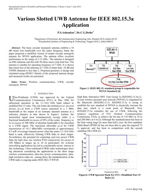
Figure 1: IEEE 802.15, standard group is responsible for<br />
WPAN Standard [4]<br />
High Rate Alternative PHY Task Group 3a (IEEE802.15.3a) [1,<br />
2] and wireless personal area network (WPAN) is originated by<br />
the Bluetooth (IEEE802.15.1). IEEE802.15.3a is trying to<br />
establish the new standard of WPAN to drastically increase the<br />
data rate, which is a weak point of Bluetooth. Now<br />
IEEE802.15.3a considers the use of UWB, following the<br />
tentative regulation of FCC (Federal Communications<br />
Commission, USA), to achieve the bit rate of 110 Mb/s at 10 m<br />
and 200 Mb/s at 4 m [3] Although the standardization has been at<br />
the final voting stage for more than half a year, the first candidate<br />
Multi-Band OFDM [4] has not been able to gain the required 75<br />
% approval, and has been in competition with the second<br />
candidate DS-UWB [5].<br />
Figure2: UWB Spectral Mask Per FCC (Modified) Part 15<br />
Rules [1]<br />
www.ijsrp.org
<strong>International</strong> <strong>Journal</strong> of Scientific and Research Publications, <strong>Volume</strong> 2, <strong>Issue</strong> 7, <strong>July</strong> <strong>2012</strong> 2<br />
ISSN 2250-3153<br />
Ultra wideband (UWB) is a leading candidate for shortrange,<br />
wireless personal area networks, or WPANs. With this<br />
technology, people will be sharing photos, music, video, data and<br />
voice among networked consumer electronics, PCs and mobile<br />
devices throughout the home and even remotely. For example,<br />
users will be able to stream video content from a PC or consumer<br />
electronics (CE) device, such as a camcorder, DVD player or<br />
personal video recorder, to a flat screen HDTV (high-definition<br />
television) display without the use of any wires. In this<br />
application, a wireless universal series bus (W-USB) is required<br />
to replace cables and build up high speed wireless link between<br />
personal computers and other devices. The W-USB has strong<br />
demands for high performance UWB antennas which will be<br />
facing three most hallenging issues namely miniaturized size,<br />
reduced ground plane reliance, and enhanced diversity<br />
performance [1]. This paper proposes a miniaturized size of<br />
UWB antenna design to fit the existing USB dongles with a<br />
typical width of 18-22 mm. The design is based on a small<br />
printed UWB antenna [2] with dimension of 25 mm × 25 mm ×<br />
1.5 mm. A narrow strip is asymmetrically attached to the top side<br />
of the radiator to reduce the length of the radiator.<br />
A rectangular notch is asymmetrically cut from the radiator.<br />
The ground-plane effect on impedance performance of the<br />
antenna has been significantly reduced due to the notch cut from<br />
the radiator. The notch extends the effective current path and<br />
concentrates majority of the current on the radiator instead of the<br />
system ground plane. This idea is an effective method to alleviate<br />
the problem of the ground plane reliance. This small printed<br />
antenna should be reduced further in order to fit within the W-<br />
USB dongle. The study of the UWB radio had started from the<br />
impulse radio which is advantageous in the hardware simplicity<br />
[1,20,21] but more complicated systems such as MB-OFDM and<br />
DS-UWB are considered now. In MB-OFDM system, a sub-band<br />
with 128 OFDM carriers occupies 528 MHz band, and different<br />
sub-bands are selected from time to time to achieve the<br />
frequency hopping (FH). Contrary, DS-UWB uses only two subbands<br />
to avoid IEEE802.11a band, i.e. the mandatory low band<br />
with 2.05 GHz bandwidth and the optional high band with 4.775<br />
GHz bandwidth, which is more like the impulse radio. Recently,<br />
another task group IEEE802.15.4a has formed to standardize the<br />
low rate PHY using UWB [1,20,21]. It focuses on the high<br />
precision ranging, as well as the communications, with ultra low<br />
power, longer range, and lower cost. Properties and the antenna<br />
related issues.<br />
A. IEEE 802.15 WPAN STANDARDS:<br />
Originally, the IEEE 802.15 group was the Bluetooth<br />
group, but it has evolved to include other short-range Wireless<br />
Personal Area Network (WPAN) systems. The initial version,<br />
802.15.1, was adapted from the Bluetooth specification and is<br />
fully compatible with Bluetooth 1.1. As it is now described by<br />
the IEEE, “The IEEE 802.15 Working Group proposes two<br />
general categories of 802.15, called TG4 (low rate) and TG3<br />
(high rate). The TG4 version provides data speeds of 20 Kbps or<br />
250 Kbps. The TG3 version supports data speeds ranging from<br />
11 Mbps to 55 Mbps. Additional features include the use of up to<br />
254 network devices, dynamic device addressing, support for<br />
devices in which latency is critical, full handshaking, security<br />
provisions, and power management. There will be 16 channels in<br />
the 2.4-GHz band, 10 channels in the 915-MHz band, and one<br />
channel in the 868-MHz band.” The 802.15.3 Standard for high<br />
data rate services, which continues to be reviewed and enhanced,<br />
includes the following features and goals: • Data rates of 11, 22,<br />
33, 44 and 55 Mbps.<br />
• Quality of Service (QoS) isochronous protocol<br />
• Ad hoc peer-to-peer networking<br />
• Security<br />
• Low power consumption<br />
• Low cost<br />
The higher data rate of this standard is designed to meet the<br />
requirements of portable consumer imaging and multimedia<br />
applications. The IEEE 802.15 Task Group 5 is studying mesh<br />
networking, determining the necessary mechanisms that must be<br />
present in the PHY and MAC layers of WPANs to enable mesh<br />
networking, in both full mesh and partial mesh topologies. Mesh<br />
networks are useful for intending network coverage without<br />
increasing transmit power or receive sensitivity, enhancing<br />
reliability with redundant routing, easy network configuration<br />
and, ultimately, longer device battery life due to fewer<br />
retransmissions. The IEEE 802.15.3 Study Group 3c, formed in<br />
March 2004, is developing a millimeter-wave-based alternative<br />
physical layer (PHY) for the existing 802.15.3 WPAN Standard<br />
802.15.3-2003. This mm- Wave WPAN will operate in a band<br />
that includes the 57-64 GHz unlicensed band. The millimeterwave<br />
WPAN will allow very high data rate applications such as<br />
high-speed internet access, streaming content download (video<br />
on demand, HDTV, home theater, etc.), real time streaming and<br />
wireless data bus for cable replacement. Optional data rates in<br />
excess of 2 Gbps are to be provided.<br />
Table 1: lists a variety of wireless applications in the WPAN<br />
space and their estimated requirements for data rates.<br />
Table1: Estimated Data rates for various WPAN applications<br />
[21, 22, 23]<br />
II. REVIEW OF THE STATE-OF-ART<br />
The concept of ultra wideband communication originated in<br />
the early days of radio. In the 1900s, the Marconi spark gap<br />
transmitter (the beginning of radio) communicated by spreading<br />
a signal over a very wide bandwidth. This use of spectrum did<br />
not allow for sharing, so the communications world abandoned<br />
wideband communication in favor of narrowband or tuned<br />
communication in which the FCC governed spectrum allocation.<br />
The FCC provides guidelines for radiated power in the<br />
www.ijsrp.org
<strong>International</strong> <strong>Journal</strong> of Scientific and Research Publications, <strong>Volume</strong> 2, <strong>Issue</strong> 7, <strong>July</strong> <strong>2012</strong> 3<br />
ISSN 2250-3153<br />
bandwidths of these communications systems and for incidental<br />
out of band radiated power. This incidental radiated power limits<br />
were the motivation for various organizations to challenge the<br />
paradigm of narrowband communications, in an ongoing effort to<br />
squeeze capacity out of a highly regulated spectrum. The<br />
Shannon-Hartley theorem states that channel capacity grows<br />
linearly with increases in bandwidth and decreases<br />
logarithmically with decreases in the signal to noise ratio (SNR).<br />
Although this relation is only exact under a considerable caveat,<br />
it does suggest how capacity is an impetus for UWB<br />
communication. Many companies argued that they should be<br />
allowed to intentionally transmit at the incidental radiated power<br />
limits (where they could already transmit accidentally) over an<br />
ultra-wide bandwidth to take advantage of this capacity potential.<br />
This argument was the motivation for the FCC approval of UWB<br />
devices. In February of 2002, the FCC amended their Part 15<br />
rules (concerning unlicensed radio devices) to include the<br />
operation of UWB devices without a license. The FCC defines<br />
UWB signals as having a fractional bandwidth of greater than<br />
0.20 or a UWB bandwidth greater than 500 MHz. UWB<br />
bandwidth is defined as “the frequency band bounded by the<br />
points that are 10 dB below the highest radiated emission”<br />
[1,3,4,24]<br />
.<br />
Figure3: Spectrum of UWB Signal Compared with Wi-Fi<br />
(802.11a) Signal [21, 22].<br />
The FCC ruling allows UWB communication devices to<br />
operate at low power (an EIRP of -41.3 dBm/MHz) in an<br />
unlicensed spectrum from 3.1 to 10.6 GHz (see Figure 1). The<br />
low emission limits for UWB are to ensure that UWB devices do<br />
not cause harmful interference to (i.e. coexist with) “licensed<br />
services and other important radio operations” [1,20,21] (e.g.<br />
802.11a devices).<br />
A. IMPORTANT PARAMETERS IN THE DESIGN OF<br />
UWB ANTENNA FOR WPAN APPLICATION:<br />
The following properties are required for the UWB<br />
antennas: Linear phase and constant group delay in directivity:<br />
If the group delay is not constant, the pulse waveform is spread<br />
out in the time domain. Low return loss over ultra wide<br />
bandwidth: If there are mismatches both at the antenna end and<br />
the circuitry end, the overall dispersion characteristic is much<br />
degraded due to the multipath within the feeding cable. Constant<br />
directivity over ultra wide bandwidth: The variation of the<br />
directivity according to the frequency results in the ripples of the<br />
frequency transfer function in some citation direction. The<br />
dispersion characteristic is then degraded. There are two<br />
fundamental principles to achieve the broadband or UWB<br />
property of the antennas [9]:<br />
1.1 SELF SIMILARITY ANTENNA: A self similarity antenna<br />
is with the constant electric shape over the wide frequency<br />
bandwidth. Here, the electric shape means the shape described in<br />
the dimension of the wavelength. A biconical antenna, a bow-tie<br />
antenna, a discone antenna, an equiangular spiral antenna are the<br />
examples of this class.<br />
1.2 SELF COMPLEMENTARY ANTENNA: A self<br />
complementary antenna is usually composed of planar<br />
conductor(s), and its complementary structure is identical to the<br />
original structure. Here, complementary structure is obtained by<br />
replacing the conductor and the non-conductor parts in the plane.<br />
Among the self complementary antennas, the log-periodic<br />
antenna is well known. Note that both structures require the<br />
infinite size of the conductor. The shape is therefore truncated in<br />
reality, and it limits the lower bound of the bandwidth.<br />
III. ANTENNA DESIGN AND CONFIGURATION<br />
Figure 4 shows the evolution of the proposed printed<br />
monopole antenna. The structure is evolved from the circular<br />
monopole radiator to annular ring shaped radiator.<br />
Circular semicircular AUD (proposed)<br />
Figure 4: Evolution of the proposed dual band antenna.<br />
a) Whole structure (b) Top view c) Bottom view<br />
Figure5: Geometry of circular monopole antenna<br />
www.ijsrp.org
<strong>International</strong> <strong>Journal</strong> of Scientific and Research Publications, <strong>Volume</strong> 2, <strong>Issue</strong> 7, <strong>July</strong> <strong>2012</strong> 4<br />
ISSN 2250-3153<br />
Figure 6: Geometry of Basic antenna<br />
The geometry of the proposed antenna is shown in Fig. 4 is<br />
fed by a 50- microstrip line and fabricated on a 1.6-mm-thick<br />
FR4 substrate with 25× 25 mm surface area. The relative<br />
permittivity and loss tangent of the substrate is 4.4 and 0.02,<br />
respectively. The antenna structure is a variation of a circular<br />
monopole antenna. The radius ( r) of the circular monopole [10]<br />
is obtained by using the equation no 1.<br />
Where g is the gap between the radiating patch and ground<br />
plane, and fL is the lowest resonant frequency corresponding to<br />
VSWR=2 .<br />
The resonant frequency of a TMnm mode is<br />
The first five values of Xnm are:<br />
Equation 2, which is based on the perfect magnetic wall<br />
assumption, yields resonant frequencies which differ from<br />
measurements by about 20%. To take into account the effect of<br />
fringing field, an effective radius was introduced. This was<br />
obtained by considering the radius of an ideal circular parallel<br />
plate capacitor which would yield the same static capacitance<br />
after fringing is taken into account. A detailed calculation yields<br />
the formula.<br />
Using ae , the resonant frequency formula becomes<br />
Equation 4 yields theoretical resonant frequencies which are<br />
within 2.5% of measured values.<br />
Table 2. Optimum dimensions of the Basic design antenna<br />
(all dimensions are in mm).<br />
SLOTS Wr1 Lr1 Wr2 Lr2 Wr3 Lr3<br />
L-slot 2.5 7 6.5 1.8 ---- ---<br />
T-slot 4 2 1.5 6 --- ---<br />
U-slot 1.5 3 7 1.5 1.5 3<br />
IV. PARAMENTRIC STUDY<br />
Parametric study has been conducted to optimize the design<br />
of the antenna. This study is crucial as it gives approximation<br />
measure before antenna fabrication can be done. The<br />
performance of annular shaped dual band antenna with WLAN<br />
band notched characteristic depends on number of parameters,<br />
such as gap (g) between radiating patch and ground plane, width<br />
(ws) and length (ls) of the substrate,length and width of the<br />
ground plane, width (w) and length (l) of the symmetrical step<br />
slot in radiating patch ( rectangular strip inside circular annular<br />
ring and inner (r) and outer radius (R) annular ring. Beside these,<br />
antenna performance also depends on ground plane size and<br />
shape. The parameters which have significant effects on dual<br />
band with WLAN band notched characteristic are discussed and<br />
their parametric studies are reported in this section. The gap `g'<br />
between the radiating patch and the ground plane affects the<br />
impedance bandwidth as it acts as a matching network. The<br />
impedance bandwidth of the proposed antenna at different Lg is<br />
shown in Figure7. The optimum impedance bandwidth is<br />
obtained at Lg=6mm, the capacitance that results from the<br />
spacing between edge of ground plane and radiating patch<br />
reasonably balances the inductance of the antenna. Figure 8<br />
shows return loss S11 (dB)<br />
Figure7: Simulated return loss (S11) curves of Circular<br />
monopole antenna for different ground length<br />
www.ijsrp.org
<strong>International</strong> <strong>Journal</strong> of Scientific and Research Publications, <strong>Volume</strong> 2, <strong>Issue</strong> 7, <strong>July</strong> <strong>2012</strong> 5<br />
ISSN 2250-3153<br />
BAND NOTCH CHARACTERISTICS USING DIFFERENT<br />
SHAPE SLOTS:<br />
To achieve the desired WLAN band notched characteristics,<br />
a T, U, L-shaped slots on the radiating patch is etched. The<br />
dimensions of quarter-wave resonating (mention-shaped) slot at<br />
central band-notched frequency can be postulated as<br />
Figure8: Basic design with T slot<br />
It is observed that for Lgnd of 6 mm, the antenna is able to<br />
operate as a narrowband antenna. However, the return loss of the<br />
antenna improves dramatically when the length ground patch<br />
reduces gradually and the best result is obtained at the height of<br />
ground plane, Lgnd of 5.4 mm.<br />
The partial ground shows better return loss compared to full<br />
ground patch on the bottom because the antenna is transformed<br />
from patch-type to monopole-type by the partial ground. In order<br />
to further improve its overall bandwidth two steps of feed line<br />
can be used but that may be used for different application. The<br />
feed line is connected to SMA center pin with width of 3 mm<br />
.<br />
Figure 9: Surface current distributions of basic antenna at<br />
3, 5 and 7 GHz<br />
Figure10: radiation patterns in the φ =0 ◦ and φ =90 ◦ planes of<br />
a proposed patch with εr =4.4 at 3, 5,7GHZ<br />
Figure11: Basic design with U slot<br />
Figure12: Surface current distributions of basic shape<br />
antenna at 3, 5 and 7 GHz<br />
Figure13: radiation patterns in the φ =0 ◦ and φ =90 ◦ planes of<br />
a proposed patch with εr =4.4 at 3,5,7GHZ<br />
www.ijsrp.org
<strong>International</strong> <strong>Journal</strong> of Scientific and Research Publications, <strong>Volume</strong> 2, <strong>Issue</strong> 7, <strong>July</strong> <strong>2012</strong> 6<br />
ISSN 2250-3153<br />
Figure14: Basic design with L slot<br />
Figure15: Surface current distributions of basic antenna at 3,<br />
5 and 7 GHz<br />
Figure16: radiation patterns in the φ =0 ◦ and φ =90 ◦ planes of<br />
a proposed patch with εr =4.4 at 3,5,7GHZ<br />
Varies slotted antenna is reported and studied. The antenna<br />
is analyzes from their current distribution and radiation pattern<br />
behavior. The required band width which could be used for<br />
Bluetooth (2.4-2.484 GHz) and UWB (3.1-10.6 GHz)<br />
applications with WLAN (5.15-5.825 GHz) band-notched<br />
characteristics could not achieved with above slots. The<br />
modification in the basic design is done to achieve the desired<br />
band.<br />
Figure17: Simulated return loss (S11) curves of all four ant at<br />
Lg=5mm.<br />
V.MODIFICATION IN THE BASIC DESIGN TO<br />
ACHIEVE PROPOSED ANTENNA:<br />
(a) (b)<br />
(c)<br />
Figure18: Geometry of proposed antenna for UWB<br />
communication (a) Top View (b) bottom View (C) Design<br />
geometry<br />
The antenna structure is fabricated on a printed circuit<br />
board (PCB) using Photolithography technique and tested. The<br />
fabricated antenna is shown in Figure11. Below fig clearly show<br />
the process for S11 (dB) measurement. The measured results<br />
reasonably agree with simulated results. The proposed antenna<br />
rejects the WLAN band and still performs good impedance<br />
matching over the UWB band.<br />
www.ijsrp.org
<strong>International</strong> <strong>Journal</strong> of Scientific and Research Publications, <strong>Volume</strong> 2, <strong>Issue</strong> 7, <strong>July</strong> <strong>2012</strong> 7<br />
ISSN 2250-3153<br />
(a) Top View (b) Bottom View<br />
(c) Antenna under Test<br />
Figure19:.Photograph of the proposed antenna<br />
Table3. Optimum dimensions of the proposed antenna (all<br />
dimensions are in mm).<br />
V. CONCLUSION<br />
A User centric concept in mobile communication has<br />
attracted increasing interest and attention recently. Future<br />
communication systems are driven by the concept of being<br />
connected anywhere anytime. These systems are powered by the<br />
emergence of small and lightweight wireless systems such as<br />
Bluetooth and UWB enabled devices. Since power required for<br />
small wireless devices is at very low level so the UWB antenna is<br />
a good candidature for WPAN applications. In this paper a<br />
simple, low-cost, and compact printed Trisul shaped dual-band<br />
antenna is proposed. This microstrip line fed antenna can be<br />
easily integrated within the printed circuit boards (PCBs) of<br />
various systems. Dimensions of the central arm govern the<br />
Bluetooth band, while dimensions of ground plane govern the<br />
UWB band. Hence, the proposed antenna provides effective<br />
control over two operating bands. The antenna provides more<br />
than 80% antenna efficiency, and its gain varies from 3–6 dB<br />
over two bands. The antenna has nearly omni directional<br />
radiation pattern, which indicates that the proposed antenna is<br />
suitable and a good candidate for Bluetooth and UWB<br />
applications.<br />
REFERENCES<br />
[1] “Federal Communications Commission revision of Part 15 of the commission’s<br />
rules regarding ultra-widebandtransmission systems,”<br />
FCC,Washington, DC, First Report and Order FCC, 02.V48, 2002.<br />
[2] C. A. Balanis, Antenna theory analysis and design, John Wiley, c1997<br />
[3] H. Schantz, “The Art and Science of U ltra-wideband Antennas”, London,<br />
Artech House,2005.<br />
[4] I. J. Bahl and P. Bhartia, Microstrip Antennas, Chapter 3, Artech<br />
House,1980.<br />
[5] Z. N. Chen “Antennas for Portable Devices,” Institute for Infocomm<br />
Research Singapore, New York, John Wiley&Sons Inc, 2007.<br />
[6] X.L. Bao and M.J. Ammann, Investigation on UWB printed monopole<br />
antenna with rectangular slitted ground plane, Microw Opt Technol Lett 49<br />
(2007), 1585–1587.<br />
[7] Q.X. Chu and Y.Y. Yang, A compact ultra-wideband antenna with 3.4/5.5<br />
GHz dual band-notched characteristics, IEEE Trans Anten-nas Propag 56<br />
(2008), 3637–3644.<br />
[8] L. Luo, Z. Cui, J.P. Xiong, X.M. Zhang, and Y.C. Jiao, Compact printed<br />
ultra-wideband monopole antenna with dual band-notch characteristic,<br />
Electron Lett 44 (2008), 1106–1107.<br />
[9] T. Yuan, C.W. Qiu, L.W. Li, M.S. Leong, and Q. Zhang, Ellipti-cally<br />
shaped ultra-wideband patch antenna with band-notch fea-tures, Microw<br />
Opt Technol Lett 50 (2008), 736–738.<br />
[10] G. Kumar and K. P. Ray , Broadband Microstrip Antennas. Norwood, MA:<br />
Artech house, 2003.<br />
[11] L. Yang;and G. B.Giannakis, Ultra-wideband communications: an idea<br />
whose time has come, IEEESignal Processing Magazine,pp.26–54, Nov.<br />
2004<br />
[12] Lin, Y. C. and K. J. Hung, \Compact ultra wideband rectangular aperture<br />
antenna and band-notched designs," IEEE Trans. Antennas Propagation,<br />
Vol. 54, No. 11, 3077-3081, 2006.<br />
[13] Chung, K., S. Hong, and J. Choi, \Ultra wide-band printed monopole<br />
antenna with band-notch filters "IET Microwaves, Antennas and Propagate,<br />
Vol. 1, No. 2, 518-522, 2007.<br />
[14] Chu, Q. X. and Y. Y. ang, \A compact ultra-wideband antenna with 3.4/5.5<br />
GHz dual band-notched characteristics," IEEE Trans. Antennas<br />
Propagation, Vol. 56, No. 12, 3637-3644,Dec. 2008.<br />
[15] Mishra, S. K., R. K. Gupta, and J. Mukherjee, \Parallel metal plated tuning<br />
fork shaped omnidirectional monopole antenna for UWB<br />
application,"Microwave Opt. Technol. Lett., Vol. 53, No. 3,601-604, Mar.<br />
2011.<br />
[16] Gao, G.-P., Z.-L. Mei, and B.-N. Li, \Novel circular slot UWB antenna with<br />
dual band-notched characteristic," Progress In Electromagnetics Research<br />
C, Vol. 15, 49-63, 2010.<br />
[17] Edalati, A. and T. A. Denidni, \A compact UWB antenna with dual bandnotched<br />
characteristics,"Microwave Opt. Tech. Lett., Vol. 52, 1183{1186,<br />
2010.<br />
[18] Gao, G.-P., M. Li, S.-F. Niu, X.-J. Li, B.-N. Li, and J.-S. Zhang,\Study of a<br />
novel wideband circular slot antenna having frequencyband-notched<br />
function,"Progress In Electromagnetics Research,Vol. 96, 141-154, 2009.<br />
[19] Luo, L., Z. Cui, J. P. Xiong, X. M. Zhang, and Y. C. Jiao, \Compact printed<br />
ultra-wideband monopole antenna with dual band-notch<br />
characteristic,"Electron. Lett., Vol. 44, No. 19, 1106- 1107, Sep. 2008.<br />
[20] Ansoft Designer, www.ansoft.com.<br />
[21] Institute of Electrical and Electronics Engineers. IEEE Std 802.15.1-2005,<br />
Wireless Medium Access Control (MAC) and Physical Layer (PHY)<br />
Specifications for Wireless Personal Area Networks (WPANs),14June2005.<br />
[22] Institute of Electrical and Electronics Engineers. IEEE Std 802.15.4-<br />
2006,Wireless Medium Access Control (MAC) and Physical Layer (PHY)<br />
Specifi-cations for Low-Rate Wireless Personal Area Networks WPANs),<br />
[23] IEEE P802.15 Study Group Medical Body Area Networks (SG-MBAN).<br />
SG BAN Montreal Interim Meeting Minutes, 20 May 2007. URL<br />
ftp://ieee:wireless@ftp.802wirelessworld.com/15/07/15-07-0748-00-0banmban-meeting-minute-montreal-may-2007.doc.<br />
[24] IEEE P802.15 Study Group Medical Body Area Networks (SG-MBAN).<br />
SG BAN San Francisco Plenary Meeting Minutes, 16 August 2007. URL<br />
ftp://ieee:wireless@ftp.802wirelessworld.com/15/07/15-07-0820-00-0banban-sessions-minute-sanfrancisco-july-2007.doc.<br />
www.ijsrp.org
<strong>International</strong> <strong>Journal</strong> of Scientific and Research Publications, <strong>Volume</strong> 2, <strong>Issue</strong> 7, <strong>July</strong> <strong>2012</strong> 8<br />
ISSN 2250-3153<br />
[25] http://www.ieee802.org/15/pub/<br />
First Author –<br />
AUTHORS<br />
Dr. Chandrasekhar G. Dethe received his<br />
M.Tech. Degree in Electronics Engineering<br />
from VNIT, Nagpur. ,and Ph.D. degree from<br />
Amravati University, Amravati.His Ph.D.<br />
Thesis titled “IP NETWORK TRAFIC<br />
MEASUREMENT, ANALYSIS AND<br />
MODELING”. He worked<br />
as an Assistant Professor at SSGM, College of Engineering<br />
Shegaon from 1999 to 2005, later on he joined as a professor and<br />
in charge of research and development activity at YCCE,<br />
Nagpur. He is currently working as a principal of PIET,<br />
Nagpur. His field of specialization includes digital<br />
communication, Data network, Signal Processing. His papers are<br />
published in National and <strong>International</strong> <strong>Journal</strong>s including IEEE<br />
proceedings. He is a fellow of IE and IETE and Life member of<br />
ISTE.<br />
Email: cgdethe@gmail.com<br />
Second Author –<br />
Mr. Pankaj S. Ashtankar obtained his<br />
Bachelor’s and master’s Degree in Electronics<br />
Engineering from RTM, Nagpur University.<br />
He is Pursuing Ph.D. in the field of UWB<br />
antenna design. He is Asst. Prof. in ECE Dept.<br />
KITS;<br />
Ramtek He attended and presented severalpapers in National,<br />
international conferences and symposium. He has been closely<br />
Associated with various continuing education programmes in the<br />
area of communication Engineering conducted by K.I.T.S,<br />
Ramtek. His area of interest is Ultra wide band and RF antenna<br />
design. He is member of IETE, Member of IE (India), Member<br />
of <strong>International</strong> Association of Engineers, Member of Antenna<br />
test and measurement society of India, Member of System<br />
society of India and Life member of ISTE.<br />
Email: psashtankar@gmail.com<br />
www.ijsrp.org